Order
Now
Product
Folder
Support &
Community
Tools &
Software
Technical
Documents
Reference
Design
LMZ20502
SNVS852D – JUNE 2012 – REVISED AUGUST 2018
LMZ20502 2-A Nano Module
1
•
•
•
•
•
•
•
1
•
•
•
•
•
•
•
Features
3 Description
Integrated Inductor
Miniature 3.5 mm × 3.5 mm × 1.75 mm Package
2-A Maximum Load Current
Input Voltage Range of 2.7 V to 5.5 V
Adjustable Output Voltage Range of 0.8 V to 3.6 V
± 1% Feedback Tolerance Over Temperature
2.4-µA (maximum) Quiescent Current In
Shutdown
3-MHz Fixed PWM Switching Frequency
–40°C to 125°C Junction Temperature Range
Power Good Flag Function
Pin-Selectable Switching Modes
Internal Compensation and Soft Start
Current Limit, Thermal Shutdown, and UVLO
Protection
Create a Custom Design Using the LMZ20502
With WEBENCH® Power Designer
The LMZ20502 nano module regulator is an easy-touse synchronous step-down DC/DC converter
capable of driving up to 2 A of load from an input of
up to 5.5 V, with exceptional efficiency and output
accuracy in a very small solution size. The innovative
package contains the regulator and inductor in a
small 3.5 mm × 3.5 mm × 1.75 mm volume, thus
saving board space and eliminating the time and
expense of inductor selection. The LMZ20502
requires only five external components and has a pinout designed for simple, optimum PCB layout. The
device provides an easy-to-use complete design with
a minimum number of external components and the
TI WEBENCH® design tool. TI's WEBENCH tool
includes features such as external component
calculation, electrical simulation, and WebTherm™.
For soldering information, refer to the following
document: SNOA401.
Device Information(1)
PART NUMBER
PACKAGE /
DRAWING
2 Applications
LMZ20502
•
•
(1) For all available packages, see the orderable addendum at
the end of the datasheet.
Point of Load Regulation
Space Constrained Applications
µSIP (8)
BODY SIZE (NOM)
3.50 mm × 3.50 mm
space
space
Simplified Schematic
EN
VIN
Typical Efficiency for VOUT = 1.8 V Auto Mode
VOUT
VOUT
100
95
VIN
RFBT
LMZ20502
90
CFF
CIN
MODE
PG
COUT
RFBB
Efficiency (%)
85
FB
GND
80
75
70
65
60
55
3V
4.2V
5V
50
45
40
0.01
0.1
1
Output Current (A)
10
C001
1
An IMPORTANT NOTICE at the end of this data sheet addresses availability, warranty, changes, use in safety-critical applications,
intellectual property matters and other important disclaimers. PRODUCTION DATA.
�LMZ20502
SNVS852D – JUNE 2012 – REVISED AUGUST 2018
www.ti.com
Table of Contents
1
2
3
4
5
6
7
Features ..................................................................
Applications ...........................................................
Description .............................................................
Revision History.....................................................
Pin Configuration and Functions .........................
Specifications.........................................................
1
1
1
2
3
4
6.1
6.2
6.3
6.4
6.5
6.6
6.7
4
4
4
5
6
7
8
Absolute Maximum Ratings ......................................
ESD Ratings ............................................................
Recommended Operating Conditions.......................
Thermal Information ..................................................
Electrical Characteristics...........................................
System Characteristics ............................................
Typical Characteristics ..............................................
Detailed Description .............................................. 9
7.1
7.2
7.3
7.4
Overview ................................................................... 9
Functional Block Diagram ......................................... 9
Feature Description................................................... 9
Device Functional Modes........................................ 13
8
Application and Implementation ........................ 15
8.1 Application Information............................................ 15
8.2 Typical Application ................................................. 16
8.3 Do's and Don'ts ...................................................... 23
9 Power Supply Recommendations...................... 23
10 Layout................................................................... 24
10.1 Layout Guidelines ................................................. 24
10.2 Layout Example .................................................... 25
10.3 Soldering Information ............................................ 25
11 Device and Documentation Support ................. 27
11.1
11.2
11.3
11.4
11.5
11.6
Device Support......................................................
Receiving Notification of Documentation Updates
Community Resources..........................................
Trademarks ...........................................................
Electrostatic Discharge Caution ............................
Glossary ................................................................
27
28
28
28
28
28
12 Mechanical, Packaging, and Orderable
Information ........................................................... 28
12.1 Tape and Reel Information ................................... 29
4 Revision History
NOTE: Page numbers for previous revisions may differ from page numbers in the current version.
Changes from Revision C (April 2015) to Revision D
•
Remove Simple Switcher branding; add links for WEBENCH, top navigator icon for TI reference design, and T&R
content ................................................................................................................................................................................... 1
Changes from Revision B (December 2014) to Revision C
•
2
Page
Added the package option addendum manually ................................................................................................................... 1
Changes from Revision A (July 2013) to Revision B
•
Page
Page
Changed Device Information and Handling Rating tables, Feature Description, Device Functional Modes,
Application and Implementation, Power Supply Recommendations, Layout, Device and Documentation Support, and
Mechanical, Packaging, and Orderable Information sections; moved some curves to Application Curves section .............. 1
Submit Documentation Feedback
Copyright © 2012–2018, Texas Instruments Incorporated
Product Folder Links: LMZ20502
�LMZ20502
www.ti.com
SNVS852D – JUNE 2012 – REVISED AUGUST 2018
5 Pin Configuration and Functions
USIP Package
8 Pin SIL
Top View
PG
EN
MODE
FB
VIN
NC
1
8
2
7
3
6
GND
4
5
VOUT
Pin Functions
PIN
NUMBER
NAME
TYPE (1)
DESCRIPTION
1
PG
O
Power good flag; open drain. Connect to logic supply through a resistor. High = power good; Low =
power bad. If not used, leave unconnected.
2
EN
I
Enable input. High = On, Low = Off. A valid input voltage, on pin 8, must be present before EN is
asserted. Do not float.
3
MODE
I
Mode selection input. High = forced PWM. Low = AUTO mode, with PFM at light load . Do not float.
4
FB
I
Feedback input to controller. Connect to output through feedback divider.
5
VOUT
P
Regulated output voltage; connect to COUT.
6
GND
G
Ground for all circuitry. Reference point for all voltages.
7
NC
8
VIN
P
Input supply to regulator. Connect to input capacitor(s) as close as possible to the VIN pin and GND
pin of the module.
EP
EP
G
Ground and heat-sink connection. See Layout Guidelines section for more information.
(1)
This pin must be left floating. Do not connect to ground or any other node.
G = Ground, I = Input, O = Output, P = Power
Submit Documentation Feedback
Copyright © 2012–2018, Texas Instruments Incorporated
Product Folder Links: LMZ20502
3
�LMZ20502
SNVS852D – JUNE 2012 – REVISED AUGUST 2018
www.ti.com
6 Specifications
6.1 Absolute Maximum Ratings
Under the recommended operating junction temperature range of -40°C to 125°C (unless otherwise noted)
(1)
MIN
MAX
VIN to GND
–0.2
6
EN, MODE, FB, PG, to GND (2)
–0.2
VIN+0.2
VOUT to GND (2)
–0.2
VIN+0.2
Junction temperature
(3)
°C
260
Storage temperature range
(3)
°C
240
Peak soldering reflow temperature for No-Pb (3)
(2)
V
150
Peak soldering reflow temperature for Pb
(1)
UNIT
–65
150
°C
Stresses beyond those listed under Absolute Maximum Ratings may cause permanent damage to the device. These are stress ratings
only, which do not imply functional operation of the device at these or any other conditions beyond those indicated under Recommended
Operating Conditions. Exposure to absolute-maximum-rated conditions for extended periods may affect device reliability.
The absolute maximum voltage on this pin must not exceed 6V with respect to ground. Do not allow the voltage on the output pin to
exceed the voltage on the input pin by more than 0.2 V.
For soldering information, refer to the following document: SNOA401.
6.2 ESD Ratings
VALUE
V(ESD)
(1)
(2)
Electrostatic discharge
Human body model (HBM), per ANSI/ESDA/JEDEC JS-001, all pins (1)
±2000
Charged-device model (CDM), per JEDEC specification JESD22-C101,
all pins (2)
±500
UNIT
V
JEDEC document JEP155 states that 500-V HBM allows safe manufacturing with a standard ESD control process.
JEDEC document JEP157 states that 250-V CDM allows safe manufacturing with a standard ESD control process.
6.3 Recommended Operating Conditions
Under the recommended operating junction temperature range of -40°C to 125°C (unless otherwise noted)
MIN
NOM
(1)
MAX
UNIT
Input voltage
2.7
5.5
V
Output voltage programming
0.8
3.6
V
V
Output voltage range
(2)
0
3.6
Load current
0
2
A
Power good flag current
0
4
mA
-40
125
°C
Junction temperature
(1)
(2)
4
Stresses beyond those listed under Absolute Maximum Ratings may cause permanent damage to the device. These are stress ratings
only, which do not imply functional operation of the device at these or any other conditions beyond those indicated under Recommended
Operating Conditions. Exposure to absolute-maximum-rated conditions for extended periods may affect device reliability.
Under no conditions should the output voltage be allowed to fall below zero volts.
Submit Documentation Feedback
Copyright © 2012–2018, Texas Instruments Incorporated
Product Folder Links: LMZ20502
�LMZ20502
www.ti.com
SNVS852D – JUNE 2012 – REVISED AUGUST 2018
6.4 Thermal Information
LMZ20502
THERMAL METRIC (1)
USIP (SIL)
UNIT
8 PINS
RθJA
Junction-to-ambient thermal resistance
42.6
RθJC(top)
Junction-to-case (top) thermal resistance
20.8
RθJB
Junction-to-board thermal resistance
9.4
ψJT
Junction-to-top characterization parameter
1.5
ψJB
Junction-to-board characterization parameter
9.3
RθJC(bot)
Junction-to-case (bottom) thermal resistance
1.8
(1)
°C/W
The values given in this table are only valid for comparison with other packages and can not be used for design purposes. For design
information please see the Maximum Ambient Temperature section. For more information about traditional and new thermal metrics, see
the Semiconductor and IC Package Thermal Metrics application report.
Submit Documentation Feedback
Copyright © 2012–2018, Texas Instruments Incorporated
Product Folder Links: LMZ20502
5
�LMZ20502
SNVS852D – JUNE 2012 – REVISED AUGUST 2018
www.ti.com
6.5 Electrical Characteristics
Limits apply over the recommended operating junction temperature range of –40°C to 125°C, unless otherwise noted.
Minimum and maximum limits are verified through test, design, or statistical correlation. Typical values represent the most
likely parametric norm at TJ = 25°C, and are provided for reference purposes only. Unless otherwise stated the following
conditions apply: VIN = 3.6 V
PARAMETER
TEST CONDITIONS
(1)
TYP
MAX (1)
0.594
MIN
UNIT
VFB
Feedback voltage
VIN = 3.6 V
0.6
0.606
V
IQ_AUTO
Operating quiescent current in
AUTO mode
AUTO mode, VFB = 0.8V
72
90
µA
IQ_PWM
Operating quiescent current in
forced PWM mode
PWM mode, VFB = 0.8V
490
620
µA
(2)
VIN = 3.6 V, VEN = 0.0 V
0.7
1.5
VIN = 5.5 V, VEN = 0.0 V
1.0
2.4
Input supply under-voltage
lock-out thresholds
Rising
2.5
Falling
2.3
High Level Input Voltage
VIH
Low Level Input Voltage
VIL
High Level Input Voltage
VIH
Low Level Input Voltage
VIL
IQ_off
VUVLO
VEN
VMODE
Shutdown quiescent current
0.4
1.2
0.4
Peak switch current limit (3)
2.1
2.7
Fosc
Internal oscillator frequency
2.5
3.0
TON
Minimum switch on-time (4)
Tss
Soft start time (4)
RPG
Power good flag pull-down
Rdson
VPG1
Power good flag, undervoltage trip (5)
% of feedback voltage, rising
VPG2
Power good flag, undervoltage trip (5)
% of feedback voltage, falling
VPG3
Power good flag, over-voltage
trip (5)
% of feedback voltage, rising
VPG4
Power good flag, over-voltage
trip (5)
% of feedback voltage, falling
TSD
Thermal shutdown (4)
Rising threshold
40
Thermal shutdown
hysteresis (4)
(1)
(2)
(3)
(4)
(5)
6
V
1.4
I LIM
µA
V
V
A
3.2
MHz
50
ns
800
µs
70
110
Ω
92%
88%
112%
108%
159
°C
15
°C
MIN and MAX limits are 100% production tested at 25°C. Limits over the operating temperature range are verified through correlation
using Statistical Quality Control (SQC) methods. Limits are used to calculate Average Outgoing Quality Level (AOQL).
Shutdown current includes leakage current of the switching transistors.
This is the peak switch current limit measured with a slow current ramp. Due to inherent delays in the current limit comparator, the peak
current limit measured at 3MHz will be larger.
This parameter is not tested in production.
See Power Good Flag Function for explanation of voltage levels.
Submit Documentation Feedback
Copyright © 2012–2018, Texas Instruments Incorporated
Product Folder Links: LMZ20502
�LMZ20502
www.ti.com
SNVS852D – JUNE 2012 – REVISED AUGUST 2018
6.6 System Characteristics
The following specifications apply to the circuit found in Figure 16 with the appropriate modifications from Table 2. These
parameters are not tested in production and represent typical performance only. Unless otherwise stated the following
conditions apply: TA = 25°C.
PARAMETER
Load
Regulation
Line
Regulation
VR-PWM
VR-PFM
Load
Transient
Line
Transient
Percent output voltage change
for the given load current change
Percent output voltage change
for the given change in input
voltage
Output voltage ripple in PWM
Output voltage ripple in PFM
Output voltage deviation from
nominal due to a load current
step
Output voltage deviation due to
an input voltage step
Peak efficiency
η
Full load efficiency
TEST CONDITIONS
MIN
TYP
VOUT = 1.2 V,
VIN = 5 V, IOUT = 0 A to 2 A, PWM
0.4%
VOUT = 1.8 V
VIN = 5 V, IOUT = 0 A to 2 A, PWM
0.4%
VOUT = 3.3 V
VIN = 5 V, IOUT = 0 A to 2 A, PWM
0.2%
VOUT = 1.2 V
IOUT = 2 A, VIN = 3 V to 5 V, PWM
0.2%
VOUT = 1.8 V
IOUT = 2 A, VIN = 3 V to 5 V, PWM
0.15%
VOUT = 3.3 V
IOUT = 2 A,VIN = 4 V to 5 V, PWM
0.18%
VOUT = 1.2 V
IOUT = 1 A, VIN = 5 V, PWM
3.3
VOUT = 1.8 V
IOUT = 1 A, VIN = 5 V, PWM
3.3
VOUT = 3.3V
IOUT= 1 A, VIN = 5 V, PWM
4.2
VOUT = 1.2V
IOUT= 1 mA, VIN = 3 V, PFM
22
VOUT = 1.8 V
IOUT= 1 mA, VIN=3 V, PFM
22
VOUT = 3.3 V
IOUT = 1 mA, VIN = 5 V, PFM
40
VOUT = 1.2 V
VIN = 5 V, IOUT = 0 A to 2 A, Tr = Tf = 2 µs,
PWM
±115
VOUT = 1.8 V
VIN = 5 V, IOUT = 0 A to 2 A, Tr = Tf = 2 µs,
PWM
±100
VOUT = 3.3 V
VIN = 5 V, IOUT = 0 A to 2 A, Tr = Tf = 2 µs,
PWM
±150
VOUT = 1.2V
IOUT = 1 A, VIN = 3 V to 5 V, Tr = Tf = 50
µs, PWM
25
VOUT = 1.8 V
IOUT = 1 A, VIN = 3 V to 5 V, Tr = Tf = 50
µs, PWM
30
VOUT = 3.3 V
IOUT = 1 A, VIN = 4 V to 5 V, Tr = Tf = 50
µs, PWM
20
VOUT = 1.2 V
VIN = 3 V
87%
VOUT = 1.8 V
VIN = 3 V
91%
VOUT = 3.3 V
VIN = 4.2 V
94%
VOUT = 1.2 V
VIN = 3 V, IOUT = 2 A
74%
VOUT = 1.8 V
VIN = 3 V, IOUT = 2 A
79%
VOUT = 3.3 V
VIN = 4.2 V, IOUT = 2 A
89%
MAX
UNIT
mV pk-pk
mV pk-pk
mV
mV pk-pk
Submit Documentation Feedback
Copyright © 2012–2018, Texas Instruments Incorporated
Product Folder Links: LMZ20502
7
�LMZ20502
SNVS852D – JUNE 2012 – REVISED AUGUST 2018
www.ti.com
6.7 Typical Characteristics
Unless otherwise specified the following conditions apply: VIN = 3.6 V, TA = 25°C.
1.82
3.2
Iout = 0 A
Iout = 1 A
-40°C
27°C
90°C
3.1
Switching Frequency (MHz)
Output Voltage (V)
1.81
3.15
1.8
1.79
1.78
1.77
3.05
3
2.95
2.9
2.85
2.8
2.75
2.7
2.65
1.76
-40
2.6
-20
0
VIN = 3.6 V
20
40
Temperature (°C)
60
80
100
2
PWM Mode
VOUT = 1.8 V
3
3.5
4
4.5
Input Voltage (V)
VIN = 3.6 V
Figure 1. Typical Output Voltage vs Temperature
5
5.5
6
D002
IOUT = 0 A
PWM Mode
Figure 2. Switching Frequency in PWM Mode
1
1
Rising
Falling
MODE Input Thresholds (V)
0.9
EN Input Thresholds (V)
2.5
D001
0.8
0.7
0.6
0.5
0.4
-40
-20
0
20
40
Temperature (°C)
60
80
Rising
Falling
0.9
0.8
0.7
0.6
0.5
0.4
-40
100
-20
0
D003
VIN = 3.6 V
20
40
Temperature (°C)
60
80
100
D004
VIN = 3.6 V
Figure 3. EN Input Thresholds
Figure 4. MODE Input Thresholds
80
0.6
75
-40°C
27°C
90°C
0.55
Input Current (mA)
Input Current (µA)
70
65
60
55
0.5
0.45
0.4
50
-40°C
27°C
90°C
45
0.35
40
0.3
2
2.5
VFB = 0.8 V
3
3.5
4
4.5
Input Voltage (V)
5
5.5
6
AUTO Mode
2.5
VFB = 0.8 V
Figure 5. Non-Switching Input Current in AUTO Mode
8
2
D005
3
3.5
4
4.5
Input Voltage (V)
5
5.5
6
D006
PWM Mode
Figure 6. Non-Switching Input Current in PWM Mode
Submit Documentation Feedback
Copyright © 2012–2018, Texas Instruments Incorporated
Product Folder Links: LMZ20502
�LMZ20502
www.ti.com
SNVS852D – JUNE 2012 – REVISED AUGUST 2018
7 Detailed Description
7.1 Overview
The LMZ20502 Nano Module is a voltage mode buck regulator with an integrated inductor. Input voltage feedforward is used to compensate for loop gain variation with input voltage. Two operating modes allow the user to
tailor the regulator to their specific requirements. In forced PWM mode, the regulator operates as a full
synchronous device with a 3 MHz (typ.) switching frequency and very low output voltage ripple. In AUTO mode,
the regulator moves into PFM when the load current drops below the mode change threshold (see Application
Curves). In PFM, the device regulates the output voltage between wider ripple limits than in PWM. This results in
much smaller supply current than in PWM, at light loads and high efficiency. A simplified block diagram is shown
in Functional Block Diagram.
7.2 Functional Block Diagram
7.3 Feature Description
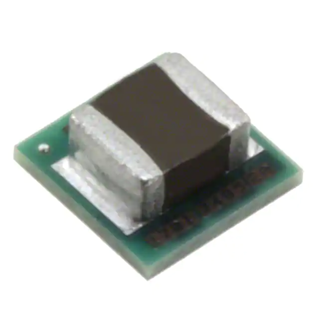
7.3.1 Nano Scale Package
The LMZ20502 incorporates world-class package technology to provide a 2 A power supply with a total volume
of only 21 mm3 (excluding external components). All that is required for a complete power supply is the addition
of feed-back resistors to set the output voltage and the input and output filter capacitors. Figure 7 and Figure 8
show the LMZ20502 package. The regulator die is embedded into a PCB substrate while the power inductor is
mounted on top. Vias and copper clad are used to make the connections to the die, inductor and the external
components. This package is MSL3 compliant.
Submit Documentation Feedback
Copyright © 2012–2018, Texas Instruments Incorporated
Product Folder Links: LMZ20502
9
�LMZ20502
SNVS852D – JUNE 2012 – REVISED AUGUST 2018
www.ti.com
Feature Description (continued)
Figure 7. Package Photo
INDUCTOR
EMBEDDED
REGULATOR
DIE
SUBSTRATE
PCB
Copper Clad
Via
Figure 8. Package Side View Drawing
7.3.2 Internal Synchronous Rectifier
The LMZ20502 uses an internal NMOS FET as a synchronous rectifier to minimize switch voltage drop and
increase efficiency. The NMOS is designed to conduct through its body diode during switch dead time. This dead
time is imposed to prevent supply current "shoot-through".
7.3.3 Current Limit Protection
The LMZ20502 incorporates cycle-by-cycle peak current limit on both the high and low side MOSFETs. This
feature limits the output current in case the output is overloaded. During the overload, the peak inductor current
is limited to that value found in the Electrical Characteristics table under the heading of "ILIM".
In addition to current limit, a short circuit protection mode is also implemented. When the feedback voltage is
brought down to less than 300 mV, but greater than 150 mV, by a short circuit, the synchronous rectifier is turned
off. This provides more voltage across the inductor to help maintain the required volt-second balance. If a
"harder" short brings the feedback voltage to below 150 mV, the current limit and switching frequency are both
reduced to about ½ of the nominal values. In addition, when the current limit is tripped, the device stops
switching for about 85 µs. At the end of the time-out, switching resumes and the cycle repeats until the short is
removed.
The effect of both overload and short circuit protection can be seen in Figure 9. This graph demonstrates that the
device will supply slightly more than 2 A to the load when in overload and much less current during fold-back
mode. This is typical behavior for any regulator with this type of current limit protection.
10
Submit Documentation Feedback
Copyright © 2012–2018, Texas Instruments Incorporated
Product Folder Links: LMZ20502
�LMZ20502
www.ti.com
SNVS852D – JUNE 2012 – REVISED AUGUST 2018
Feature Description (continued)
2.0
1.8
Output Voltage (V)
1.6
1.4
1.2
1.0
0.8
0.6
0.4
0.2
0.0
0.0
0.5
1.0
1.5
2.0
2.5
Output Current (A)
3.0
C001
Figure 9. Typical Current Limit Profile
VIN = 5 V, VOUT = 1.8 V
7.3.4 Start-Up
Start-up and shutdown of the LMZ20502 is controlled by the EN input. The characteristics of this input are found
in the Electrical Characteristics table. A valid input voltage must be present on VIN before the enable control is
asserted. The maximum voltage on the EN pin is 5.5 V or VIN, whichever is smaller. Do not allow this input to
float.
The LMZ20502 features a current limit based soft-start, that prevents large inrush currents and output overshoots
as the regulator is starting up. The peak inductor current is stepped-up in a staircase fashion during the soft start
period. A typical start-up event is shown in Figure 10:
EN
Output Voltage
2V/div
PG
Input Current
1A/div
500µs/div
Figure 10. Typical Start-Up Waveforms, VIN = 5 V,
VOUT = 3.3 V, IOUT = 1 A
7.3.5 Dropout Behavior
When the input voltage is close to the output voltage the regulator will operate at very large duty cycles. Normal
time delays of the internal circuits prevents the attainment of controlled duty cycles near 100%. In this condition
the LMZ20502 will skip switching cycles in order to maintain regulation with the highest possible input-to-output
ratio. Some increase in output voltage ripple may appear as the regulator skips cycles. As the input voltage gets
closer to the output voltage, the regulator will eventually reach 100% duty cycle, with the high side switch turned
on. The output will then follow the input voltage minus the drop across the high side switch and inductor
resistance. Figure 11 and Figure 12 show typical drop-out behavior for output voltages of 2.5 V and 3.3 V.
Submit Documentation Feedback
Copyright © 2012–2018, Texas Instruments Incorporated
Product Folder Links: LMZ20502
11
�LMZ20502
SNVS852D – JUNE 2012 – REVISED AUGUST 2018
www.ti.com
Feature Description (continued)
Since the internal gate drive levels of the LMZ20502 are dependent on input voltage, the Rdson of the power
FETs will increase at low input voltages. This will result in degraded efficiency at output currents of greater than 1
A and input voltages below about 2.9 V. Also, combinations of low input voltage and high output voltage
increases the effective switch duty cycle which may result in increased output voltage ripple.
2.6
Output Voltage (V)
2.5
2.4
2.3
2.2
2.1
0A
0.5A
1A
2A
2.0
1.9
2.0
2.2
2.4
2.6
2.8
3.0
3.2
3.4
3.6
3.8
Input Voltage (V)
4.0
C001
Figure 11. Typical Drop-Out Behavior, VOUT = 2.5 V
3.6
Output Voltage (V)
3.4
3.2
3.0
2.8
2.6
2.4
0A
0.5A
1A
2A
2.2
2.0
2.6
2.8
3.0
3.2
3.4
3.6
Input Voltage (V)
3.8
4.0
C001
Figure 12. Typical Drop-Out Behavior, VOUT = 3.3 V
7.3.6 Power Good Flag Function
The operation of the power good flag function is described in the diagram shown in Figure 13.
12
Submit Documentation Feedback
Copyright © 2012–2018, Texas Instruments Incorporated
Product Folder Links: LMZ20502
�LMZ20502
www.ti.com
SNVS852D – JUNE 2012 – REVISED AUGUST 2018
Feature Description (continued)
VOUT
PG3 = 112%
PG4 = 108%
PG1 = 92%
PG2 = 88%
PGOOD
High = Good
Low = Bad
Figure 13. Typical Power Good Flag Operation
This output consists of an open drain NMOS with an Rdson of about 70 Ω. When used, the power good flag
should be connected to a logic supply through a pull-up resistor. It can also be pulled-up to either VIN or VOUT,
through an appropriate resistor, as desired. If this function is not needed, the PG output should be left floating.
The current through this flag pin should be limited to less than 4 mA. A pull-up resistor of ≥1.5 kΩ will satisfy this
requirement. When the EN input is pulled low, the PG flag output will also be forced low, assuming a valid input
voltage is present at the VIN pin.
7.3.7 Thermal Shutdown
The LMZ20502 incorporates a thermal shutdown feature to protect the device from excessive die temperatures.
The device will stop switching when the internal die temperature reaches about 159°C. Switching will resume
when the die temperature drops to about 144°C.
7.4 Device Functional Modes
Please refer to Table 1 and the following paragraphs for a detailed description of the functional modes of the
LMZ20502. These modes are controlled by the MODE input as shown in Table 1. The maximum voltage on the
MODE pin is 5.5 V or VIN, whichever is smaller. This input must not be allowed to float.
Table 1. Mode Selection
MODE PIN VOLTAGE
OPERATION
> 1.2 V
Forced PWM: The regulator operates in constant frequency, PWM mode for all loads from
no-load to full load; no diode emulation is used.
< 0.4 V
AUTO Mode: The regulator operates in constant frequency mode for loads greater than the
mode change threshold. For loads less than the mode change threshold, the regulator
operates in PFM with diode emulation.
Submit Documentation Feedback
Copyright © 2012–2018, Texas Instruments Incorporated
Product Folder Links: LMZ20502
13
�LMZ20502
SNVS852D – JUNE 2012 – REVISED AUGUST 2018
www.ti.com
7.4.1 PWM Operation
In forced PWM mode, the converter operates as a constant frequency voltage mode regulator with input voltage
feed-forward. This provides excellent line and load regulation and low output voltage ripple. This operation is
maintained, even at no-load, by allowing the inductor current to reverse its normal direction. While in PWM mode,
the output voltage is regulated by switching at a constant frequency and modulating the duty cycle to control the
power to the load. This mode trades off reduced light load efficiency for low output voltage ripple and constant
switching frequency. In this mode, a negative current limit of about 750mA is imposed to prevent damage to the
regulator power FETs.
7.4.2 PFM Operation
When in AUTO mode, and at light loads, the device enters PFM. The regulator estimates the load current by
measuring both the high side and low side switch currents. This estimate is only approximate, and the exact load
current threshold, to trigger PFM, can vary greatly with input and output voltage. The Application Curves show
mode change thresholds for several typical operating points. When the regulator detects this threshold, the
reference voltage is increased by approximately 10 mV. This causes the output voltage to rise to meet the new
regulation point. When this point is reached, the converter stops switching and much of the internal circuitry is
shut off, while the reference is returned to the PWM value. This saves supply current while the output voltage
naturally starts to fall under the influence of the load current. When the output voltage reaches the PWM
regulation point, switching is again started and the reference voltage is again increased by about 10 mV; thus
starting the next cycle. Typical waveforms are shown in Figure 14:
Switch Voltage
2V/div
Output Voltage
50mV/div
20µs/div
Figure 14. Typical PFM Mode Waveforms: VIN = 3.6 V,
VOUT = 1.8 V, IOUT = 10 mA
90
Input Supply Current (µA)
88
86
84
82
80
78
76
74
VOUT = 1.8 V
VOUT = 3.3 V
72
70
2.5
3
3.5
4
4.5
Input Voltage (V)
5
5.5
D007
Figure 15. Typical No Load Input Supply Current
14
Submit Documentation Feedback
Copyright © 2012–2018, Texas Instruments Incorporated
Product Folder Links: LMZ20502
�LMZ20502
www.ti.com
SNVS852D – JUNE 2012 – REVISED AUGUST 2018
The actual output voltage ripple will depend on the feedback divider ratio and on the delay in the PFM
comparator. The frequency of the PFM "bursts" will depend on the input voltage, output voltage, load and output
capacitor. Within each "burst" the device switches at 3 MHz (typ.). If the load current increases above the
threshold, normal PWM operation is resumed. This mode provides high light load efficiency by reducing the
amount of supply current required to regulate the output at small load currents. This mode trades off very good
light load efficiency for larger output voltage ripple and variable switching frequency. An example of the typical
input supply current, while regulating with no load, is shown in Figure 15.
Because of normal part-to-part variation, the LMZ20502 may not switch into PFM mode at high input voltages.
This may be seen with output voltages of about 1.2 V and below, at input voltages of about 4.2 V and above.
8 Application and Implementation
NOTE
Information in the following applications sections is not part of the TI component
specification, and TI does not warrant its accuracy or completeness. TI’s customers are
responsible for determining suitability of components for their purposes. Customers should
validate and test their design implementation to confirm system functionality.
8.1 Application Information
The LMZ20502 is a step down DC-to-DC regulator. It is typically used to convert a higher DC voltage to a lower
DC voltage with a maximum output current of 2 A. The following design procedure can be used to select
components for the LMZ20502. Alternately, the WEBENCH design tool may be used to generate a complete
design. WEBENCH utilizes an iterative design procedure and has access to a comprehensive database of
components. This allows the tool to create an optimized design and allows the user to experiment with various
design options.
Submit Documentation Feedback
Copyright © 2012–2018, Texas Instruments Incorporated
Product Folder Links: LMZ20502
15
�LMZ20502
SNVS852D – JUNE 2012 – REVISED AUGUST 2018
www.ti.com
8.2 Typical Application
Figure 16 shows the minimum required application circuit, set up for a 1.8 V output. Figure 17 shows a full
featured application circuit. Please refer to Figure 16 and Figure 17 during the following design procedures.
EN
VIN
VIN
2.7V to 5.5V
VOUT
VOUT
1.8V @ 2A
LMZ20502
RFBT
CIN
2x10µF
GND
MODE
PG
CFF
80.6kŸ
16pF
COUT
FB
10µF
RFBB
40.2kŸ
Figure 16. LMZ20502 Typical Application
VOUT = 1.8 V
VIN
2.7V to 5.5V
2x10µF
100kŸ
CIN
VIN
PG
RESET
VOUT
µC
MODE
I/O
LMZ20502
VOUT
RFBT
EN
I/O
1.8V @ 2A
GND
CFF
80.6kŸ
16pF
COUT
FB
10µF
RFBB
40.2kŸ
Figure 17. LMZ20502 Full Featured Application
16
Submit Documentation Feedback
Copyright © 2012–2018, Texas Instruments Incorporated
Product Folder Links: LMZ20502
�LMZ20502
www.ti.com
SNVS852D – JUNE 2012 – REVISED AUGUST 2018
Typical Application (continued)
8.2.1 Detailed Design Procedure
8.2.1.1 Custom Design With WEBENCH® Tools
Click here to create a custom design using the LMZ20502 device with the WEBENCH® Power Designer.
1. Start by entering the input voltage (VIN), output voltage (VOUT), and output current (IOUT) requirements.
2. Optimize the design for key parameters such as efficiency, footprint, and cost using the optimizer dial.
3. Compare the generated design with other possible solutions from Texas Instruments.
The WEBENCH Power Designer provides a customized schematic along with a list of materials with real-time
pricing and component availability.
In most cases, these actions are available:
• Run electrical simulations to see important waveforms and circuit performance
• Run thermal simulations to understand board thermal performance
• Export customized schematic and layout into popular CAD formats
• Print PDF reports for the design, and share the design with colleagues
Get more information about WEBENCH tools at www.ti.com/WEBENCH.
Please refer to Table 2 while following the detailed design procedure. This procedure applies to both Figure 16
and to Figure 17. Also, the Application Curves apply to both schematics.
Table 2. Recommended Component Values (1)
VOUT (V)
RFBB (kΩ)
RFBT (kΩ)
COUT (µF)
EFFECTIVE COUT(µF) (2)
CFF (pF)
CIN (µF)
EFFECTIVE CIN (µF) (2)
0.8
121
40.2
2 x 10
18 µF
39
2 x 10
14
1.2
30.1
30.1
10
8.8 µF
20
2 x 10
14
1.8
40.2
80.6
10
8.4 µF
16
2 x 10
14
2.5
47.5
150
10
7.8 µF
12
2 x 10
14
3.3
53.2
237
10
7.1 µF
82
2 x 10
14
3.6
53.2
267
10
6.8 µF
82
2 x 10
14
(1)
(2)
CIN = COUT = 10 µF, 16 V, 0805, X7R, Samsung CL21B106KOQNNNE. COUT measured at VOUT; CIN measured at 3.3 V.
The effective value takes into account the capacitor voltage coefficient.
8.2.1.2 Setting The Output Voltage
The LMZ20502 regulates its feedback voltage to 0.6 V (typ). A feedback divider, shown in Figure 16, is used to
set the desired output voltage. Equation 1 can be used to select RFBB .
0.6
R FBB
˜ R FBT
VOUT 0.6
(1)
For best results, RFBT should be chosen between 30 kΩ and 300 kΩ. See Table 2 for recommended values for
typical output voltages.
8.2.1.3 Output and Feed-Forward Capacitors
The LMZ20502 is designed to work with low ESR ceramic capacitors. The effective value of these capacitors is
defined as the actual capacitance under voltage bias and temperature. All ceramic capacitors have large voltage
coefficients, in addition to normal tolerances and temperature coefficients. Under D.C. bias, the capacitance
value drops considerably. Larger case sizes and/or higher voltage capacitors are better in this regard. To help
mitigate these effects, multiple small capacitors can be used in parallel to bring the minimum effective
capacitance up to the desired value. This can also ease the RMS current requirements on a single capacitor.
Typically, 10 V, X5R, 0805 capacitors are adequate for the output, while 16-V caps may be used on the input.
Some recommended component values are provided in Table 2. Also, shown are the measured values of
effective input and output capacitance for the given capacitor. If smaller values of output capacitance are used,
CFF must be adjusted to give good phase margin. In any case, load transient response will be compromised with
lower values of output capacitance. Values much lower than those found in Table 2 should be avoided.
Submit Documentation Feedback
Copyright © 2012–2018, Texas Instruments Incorporated
Product Folder Links: LMZ20502
17
�LMZ20502
SNVS852D – JUNE 2012 – REVISED AUGUST 2018
www.ti.com
In practice, the output capacitor and CFF, are adjusted for the best transient response and highest loop phase
margin. Load transient testing and Bode plots are the best way to validate any given design. Application report
SLVA289 should prove helpful when optimizing the feed-forward capacitor. Also, SNVA364 details a simple
method of creating a Bode plot with basic laboratory equipment. The values of CFF found in Table 2 provide a
good starting point.
A careful study of the temperature and bias voltage variation of any candidate ceramic capacitor should be made
in order to ensure that the minimum values of effective capacitance are provided. The best way to obtain an
optimum design is to use the Texas Instruments WEBENCH tool.
The maximum value of total output capacitance should be limited to between 100 µF and 200 µF. Large values
of output capacitance can prevent the regulator from starting-up correctly and adversely affect the loop stability. If
values in the range given above, or larger, are to be used, then a careful study of start-up at full load and loop
stability must be performed.
8.2.1.4 Input Capacitors
The ceramic input capacitors provide a low impedance source to the regulator in addition to supplying ripple
current and isolating switching noise from other circuits. An effective value of at least 14 µF is normally sufficient
for the input capacitor. If the main input capacitor(s) can not be placed close to the module, then a small 10 nF to
100 nF capacitor should be placed directly at the module, across the supply and ground pins.
Many times it is desirable to use an electrolytic capacitor on the input, in parallel with the ceramics. This is
especially true if long leads/traces are used to connect the input supply to the regulator. The moderate ESR of
this capacitor can help damp any ringing on the input supply caused by long power leads. This method can also
help to reduce voltage spikes that may exceed the maximum input voltage rating of the LMZ20502. The use of
this additional capacitor will also help with voltage dips caused by input supplies with unusually high impedance.
Most of the switching current passes through the input ceramic capacitor(s). The approximate RMS value of this
current can be calculated with Equation 2 and should be checked against the manufactures maximum ratings.
I RMS |
I OUT
2
(2)
8.2.1.5 Maximum Ambient Temperature
As with any power conversion device, the LMZ20502 will dissipate internal power while operating. The effect of
this power dissipation is to raise the internal temperature of the converter, above ambient. The internal die
temperature is a function of the ambient temperature, the power loss and the effective thermal resistance RθJA of
the device and PCB combination. The maximum internal die temperature for the LMZ20502 is 125°C, thus
establishing a limit on the maximum device power dissipation and therefore load current at high ambient
temperatures. Equation 3 shows the relationships between the important parameters.
I OUT
TJ TA
˜
R -$
1
˜
1
VOUT
(3)
It is easy to see that larger ambient temperatures and larger values of RθJA will reduce the maximum available
output current. As stated in SPRA953, the values given in the Thermal Information table are not valid for design
purposes and must not be used to estimate the thermal performance of the application. The values reported in
that table were measured under a specific set of conditions that never obtain in an actual application. The
effective RθJA is a critical parameter and depends on many factors such as power dissipation, air temperature,
PCB area, copper heatsink area, air flow, and adjacent component placement. The resources found in Table 3
can be used as a guide to estimate the RθJA for a given application environment. A typical example of RθJA
versus copper board area is shown in Figure 18 . The copper area in this graph is that for each layer; the inner
layers are 1 oz. (35µm). An RθJA of 44°C/W is the approximate value for the LMZ20502 evaluation board. The
efficiency found in the equation, η, should be taken at the elevated ambient temperature. For the LMZ20502 the
efficiency is about two to three percent lower at high temperatures. Therefore, a slightly lower value than the
typical efficiency can be used in the calculation. In this way Equation 3 can be used to estimate the maximum
output current for a given ambient, or to estimate the maximum ambient for a given load current.
A typical curve of maximum load current vs. ambient temperature is shown in Figure 19. This graph assumes a
RθJA of 44°C/W and an input voltage of 5 V.
18
Submit Documentation Feedback
Copyright © 2012–2018, Texas Instruments Incorporated
Product Folder Links: LMZ20502
�LMZ20502
www.ti.com
SNVS852D – JUNE 2012 – REVISED AUGUST 2018
Thermal Resistance J-A (°C/W)
100
2-LAYER 70 µm (2 oz) Cu
4-LAYER 70 µm (2 oz) Cu
90
80
70
60
50
40
30
20
0
5
10
Copper Area (cm2)
15
20
D012
Figure 18. RθJA versus Copper Board Area
2.5
Output Current (A)
2.0
1.5
1.0
1.2V
1.8V
3.3V
0.5
0.0
40
50
60
70
80
90
100 110
Ambient Temperature (ƒC)
120 130 140
C001
Figure 19. Maximum Output Current Vs. Ambient Temperature, RθJA = 44°C/W, VIN = 5 V
8.2.1.6 Options
The circuit in Figure 17 highlights the use of the features of the LMZ20502. The PG output is open drain, and
requires a pull-up resistor to a logic supply that is commensurate with the system logic voltage levels. If a reset
function is not needed, the PG pin should be left open. The EN and MODE inputs are digital inputs, requiring
only simple logic levels for proper operation. If the system does not need to control these features, the inputs
should be connected to either VIN or GND, as appropriate. Please see Feature Description for details.
Submit Documentation Feedback
Copyright © 2012–2018, Texas Instruments Incorporated
Product Folder Links: LMZ20502
19
�LMZ20502
SNVS852D – JUNE 2012 – REVISED AUGUST 2018
www.ti.com
8.2.2 Application Curves
The following specifications apply to the circuit found in Figure 16 or Figure 17 with the appropriate modifications from
Table 2. These parameters are not tested and represent typical performance only. Unless otherwise stated the following
conditions apply: TA = 25°C.
100
95
90
Efficiency (%)
85
Output Voltage
50mV/div
80
75
70
65
60
55
Output Current
1A/div
3V
4.2V
5V
50
45
40
0.01
0.1
1
10
Output Current (A)
C001
50µs/div
VOUT = 1.8 V
VOUT = 1.8 V
Figure 21. Load Transient In PWM
Figure 20. Efficiency
1.810
3V
4.2V
5V
1.805
Output Voltage (V)
VIN = 4.2 V
Output Voltage
50mV/div
1.800
1.795
1.790
Output Current
1A/div
1.785
0.0
0.5
1.0
1.5
2.0
Output Current (A)
2.5
C003
50µs/div
VOUT = 1.8 V
VOUT = 1.8 V
VIN = 4.2 V
Figure 23. Load Transient In AUTO Mode
Figure 22. Regulation, AUTO Mode
0.35
EN
0.30
Output Current (A)
PWM
0.25
Output Voltage
1V/div
PFM
0.20
PG
0.15
0.10
Input Current
0.5A/div
0.05
0.00
2.5
3.0
3.5
4.0
4.5
5.0
Input Voltage (V)
500µs/div
5.5
C002
VOUT = 1.8 V
VOUT = 1.8 V
Figure 24. AUTO Mode Thresholds
20
Submit Documentation Feedback
VIN = 5 V
IOUT = 1 A
Figure 25. Start-Up
Copyright © 2012–2018, Texas Instruments Incorporated
Product Folder Links: LMZ20502
�LMZ20502
www.ti.com
SNVS852D – JUNE 2012 – REVISED AUGUST 2018
The following specifications apply to the circuit found in Figure 16 or Figure 17 with the appropriate modifications from
Table 2. These parameters are not tested and represent typical performance only. Unless otherwise stated the following
conditions apply: TA = 25°C.
100
95
90
Efficiency (%)
85
Output Voltage
50mV/div
80
75
70
65
60
55
3V
4.2V
5V
50
45
40
0.01
0.1
1
Output Current
1A/div
10
Output Current (A)
C004
VOUT = 1.2 V
50µs/div
VOUT = 1.2 V
Figure 26. Efficiency
Figure 27. Load Transients In PWM
1.204
3V
4.2V
5V
1.202
Output Voltage (V)
VIN = 4.2 V
1.200
Output Voltage
50mV/div
1.198
1.196
1.194
Output Current
1A/div
1.192
1.190
0.0
0.5
1.0
1.5
2.0
Output Current (A)
2.5
C005
50µs/div
VOUT = 1.2 V
VOUT = 1.2 V
Figure 28. Regulation, AUTO Mode
VIN = 4.2 V
Figure 29. Load Transients In AUTO Mode
0.30
EN
Output Current (A)
0.25
0.20
Output Voltage
1V/div
0.15
PG
PWM
0.10
PFM
Input Current
0.5A/div
0.05
0.00
2.5
3.0
3.5
4.0
4.5
5.0
5.5
500µs/div
Input Voltage (V)
C002
VOUT = 1.2 V
VOUT = 1.2 V
Figure 30. AUTO Mode Thresholds
VIN = 5V
IOUT = 1A
Figure 31. Start-up
Submit Documentation Feedback
Copyright © 2012–2018, Texas Instruments Incorporated
Product Folder Links: LMZ20502
21
�LMZ20502
SNVS852D – JUNE 2012 – REVISED AUGUST 2018
www.ti.com
The following specifications apply to the circuit found in Figure 16 or Figure 17 with the appropriate modifications from
Table 2. These parameters are not tested and represent typical performance only. Unless otherwise stated the following
conditions apply: TA = 25°C.
100
95
90
Efficiency (%)
85
80
Output Voltage
50mV/div
75
70
65
60
55
50
4.2V
45
Output Current
1A/div
5V
40
0.01
0.1
1
10
Output Current (A)
C007
VOUT = 3.3 V
50µs/div
VOUT = 3.3 V
Figure 32. Efficiency
VIN = 4.2 V
Figure 33. Load Transients In PWM
3.265
4.2V
Output Voltage (V)
3.260
5V
3.255
Output Voltage
50mV/div
3.250
3.245
3.240
3.235
Output Current
1A/div
3.230
0.0
0.5
1.0
1.5
2.0
Output Current (A)
2.5
50µs/div
C008
VOUT = 3.3 V
VOUT = 3.3 V
VIN = 4.2 V
Figure 35. Load Transients In AUTO Mode
Figure 34. Regulation, AUTO Mode
0.35
0.30
EN
Output Current (A)
PWM
0.25
Output Voltage
2V/div
0.20
PFM
0.15
PG
0.10
Input Current
1A/div
0.05
0.00
3.5
4.0
4.5
5.0
Input Voltage (V)
5.5
500µs/div
C009
VOUT = 3.3 V
VOUT = 3.3 V
VIN = 5 V
IOUT = 1 A
Figure 36. AUTO Mode Thresholds
Figure 37. Start-up
space
space
space
22
Submit Documentation Feedback
Copyright © 2012–2018, Texas Instruments Incorporated
Product Folder Links: LMZ20502
�LMZ20502
www.ti.com
SNVS852D – JUNE 2012 – REVISED AUGUST 2018
8.3 Do's and Don'ts
•
•
•
•
•
•
•
•
•
Don't: Exceed the Absolute Maximum Ratings.
Don't: Exceed the ESD Ratings .
Don't: Exceed the Recommended Operating Conditions.
Don't: Allow the EN or MODE input to float.
Don't: Allow the voltage on the EN or MODE input to exceed the voltage on the VIN pin.
Don't: Allow the output voltage to exceed the input voltage.
Don't: Use the thermal data given in the Thermal Information table to design your application.
Do: Follow all of the guidelines and/or suggestions found in this data sheet, before committing your design to
production. TI Application Engineers are ready to help critique your design and PCB layout to help make your
project a success.
Do: Refer to the helpful documents found in Table 3 and Table 4.
9 Power Supply Recommendations
The characteristics of the input supply must be compatible with the Absolute Maximum Ratings and
Recommended Operating Conditions found in this data sheet. In addition, the input supply must be capable of
delivering the required input current to the loaded regulator. The average input current can be estimated with
Equation 4
I IN
VOUT ˜ I OUT
VIN ˜
(4)
If the regulator is connected to the input supply through long wires or PCB traces, special care is required to
achieve good performance. The parasitic inductance and resistance of the input cables can have an adverse
effect on the operation of the regulator. The parasitic inductance, in combination with the low ESR ceramic input
capacitors, can form an under-damped resonant circuit. This circuit may cause over-voltage transients at the VIN
pin, each time the input supply is cycled on and off. The parasitic resistance will cause the voltage at the VIN pin
to dip when the load on the regulator is switched on, or exhibits a transient. If the regulator is operating close to
the minimum input voltage, this dip may cause the device to shutdown and/or reset. The best way to solve these
kinds of issues is to reduce the distance from the input supply to the regulator and/or use an aluminum or
tantalum input capacitor in parallel with the ceramics. The moderate ESR of these types of capacitors will help to
damp the input resonant circuit and reduce any voltage overshoots. A value in the range of 20 µF to 100 µF is
usually sufficient to provide input damping and help to hold the input voltage steady during large load transients.
Sometimes, for other system considerations, an input filter is used in front of the regulator module. This can lead
to instability, as well as some of the effects mentioned above, unless it is designed carefully. The following user
guide provides helpful suggestions when designing an input filter for any switching regulator: SNVA489.
In some cases a Transient Voltage Suppressor (TVS) is used on the input of regulators. One class of this device
has a "snap-back" V-I characteristic (thyristor type). The use of a device with this type of characteristic is not
recommend. When the TVS "fires", the clamping voltage drops to a very low value. If this holding voltage is less
than the output voltage of the regulator, the output capacitors will be discharged through the regulator back to the
input. This uncontrolled current flow could damage the regulator.
Submit Documentation Feedback
Copyright © 2012–2018, Texas Instruments Incorporated
Product Folder Links: LMZ20502
23
�LMZ20502
SNVS852D – JUNE 2012 – REVISED AUGUST 2018
www.ti.com
10 Layout
10.1 Layout Guidelines
The PCB layout of any DC/DC converter is critical to the optimal performance of the design. Bad PCB layout can
disrupt the operation of an otherwise good schematic design. Even if the converter regulates correctly, bad PCB
layout can mean the difference between a robust design and one that cannot be mass produced. Furthermore,
the EMI performance of the regulator is dependent on the PCB layout, to a great extent. In a buck converter, the
most critical PCB feature is the loop formed by the input capacitor and the module ground, as shown in
Figure 38. This loop carries fast transient currents that can cause large transient voltages when reacting with the
trace inductance. These unwanted transient voltages will disrupt the proper operation of the converter. Because
of this, the traces in this loop should be wide and short, and the loop area as small as possible to reduce the
parasitic inductance. Figure 39 shows a recommended layout for the critical components of the LMZ20502; the
top side metal is shown in red. This PCB layout is a good guide for any specific application. The following
important guidelines should also be followed:
1. Place the input capacitor CIN as close as possible to the VIN and GND terminals. VIN (pin 8) and GND
(pin 6) are on the same side of the module, simplifying the input capacitor placement.
2. Place the feedback divider as close as possible to the FB pin on the module. The divider and CFF
should be close to the module, while the length of the trace from VOUT to the divider can be somewhat
longer. However, this latter trace should not be routed near any noise sources that can capacitively couple to
the FB input.
3. Connect the EP pad to the GND plane. This pad acts as a heat-sink connection and a ground connection
for the module. It must be solidly connected to a ground plane. The integrity of this connection has a direct
bearing on the effective RθJA.
4. Provide enough PCB area for proper heat-sinking. As stated in the Maximum Ambient Temperature
section, enough copper area must be used to provide a low RθJA, commensurate with the maximum load
current and ambient temperature. The top and bottom PCB layers should be made with two ounce copper;
and no less than one ounce.
5. The resources in Table 4 provide additional important guidelines
VIN
CIN
GND
Figure 38. Current Loops With Fast Transient Currents
24
Submit Documentation Feedback
Copyright © 2012–2018, Texas Instruments Incorporated
Product Folder Links: LMZ20502
�LMZ20502
www.ti.com
SNVS852D – JUNE 2012 – REVISED AUGUST 2018
10.2 Layout Example
GND
HEATSINK
TOP
VIEW
VIN
CIN
GND
EP
COUT
VOUT
RFBB
GND
HEATSINK
RFBT
CFF
Top Trace
Bottom Trace
Figure 39. Example PCB Layout
10.3 Soldering Information
Proper operation of the LMZ20502 requires that it be correctly soldered to the PCB. This is especially true
regarding the EP. This pad acts as a quiet ground reference for the device and a heatsink connection. Use the
following recommendations when utilizing machine placement of the device:
•
•
•
•
•
•
•
Dimension of area for pick-up: 2 mm x 2.5 mm.
Use a nozzle size of less than 1.3 mm in diameter, so that the head does not touch the outer area of the
package.
Use a soft tip pick-and-place head.
Add 0.05 mm to the component thickness so that the device will be released 0.05 mm into the solder paste
without putting pressure or splashing the solder paste.
Slow the pick arm when picking the part from the tape and reel carrier and when depositing the device on the
board.
If the machine releases the component by force, use the minimum force and no more than 3 N.
For PCBs with surface mount components on both sides, it is suggested to put the LMZ20502 on the top
side. In case the application requires bottom side placement, a re-flow fixture may be required to protect the
module during the second reflow.
In addition, please follow the important guidelines found in: SNOA401. The curves in Figure 40 and Figure 41
show typical soldering temperature profiles.
Submit Documentation Feedback
Copyright © 2012–2018, Texas Instruments Incorporated
Product Folder Links: LMZ20502
25
�LMZ20502
SNVS852D – JUNE 2012 – REVISED AUGUST 2018
www.ti.com
Soldering Information (continued)
Figure 40. Typical Re-flow Profile Eutectic (63sn/37pb) Solder Paste
Figure 41. Typical Re-flow Profile Lead-Free (Sca305 Or Sac405) Solder Paste
26
Submit Documentation Feedback
Copyright © 2012–2018, Texas Instruments Incorporated
Product Folder Links: LMZ20502
�LMZ20502
www.ti.com
SNVS852D – JUNE 2012 – REVISED AUGUST 2018
11 Device and Documentation Support
11.1 Device Support
11.1.1 Third-Party Products Disclaimer
TI'S PUBLICATION OF INFORMATION REGARDING THIRD-PARTY PRODUCTS OR SERVICES DOES NOT
CONSTITUTE AN ENDORSEMENT REGARDING THE SUITABILITY OF SUCH PRODUCTS OR SERVICES
OR A WARRANTY, REPRESENTATION OR ENDORSEMENT OF SUCH PRODUCTS OR SERVICES, EITHER
ALONE OR IN COMBINATION WITH ANY TI PRODUCT OR SERVICE.
11.1.2 Development Support
11.1.2.1 Custom Design With WEBENCH® Tools
Click here to create a custom design using the LMZ20502 device with the WEBENCH® Power Designer.
1. Start by entering the input voltage (VIN), output voltage (VOUT), and output current (IOUT) requirements.
2. Optimize the design for key parameters such as efficiency, footprint, and cost using the optimizer dial.
3. Compare the generated design with other possible solutions from Texas Instruments.
The WEBENCH Power Designer provides a customized schematic along with a list of materials with real-time
pricing and component availability.
In most cases, these actions are available:
• Run electrical simulations to see important waveforms and circuit performance
• Run thermal simulations to understand board thermal performance
• Export customized schematic and layout into popular CAD formats
• Print PDF reports for the design, and share the design with colleagues
Get more information about WEBENCH tools at www.ti.com/WEBENCH.
11.1.3 Documentation Support
11.1.3.1 Related Documentation
Table 3. Resources For Estimating RθJA
TITLE
LINK
AN-2020 Thermal Design By Insight, Not
Hindsight
SNVA419
AN-2026 The Effect of PCB Design on the
Thermal Performance of SIMPLE
SWITCHER Power Modules
SNVA424
AN-1520 A Guide to Board Layout for Best
Thermal Resistance for Exposed Packages
SNVA183
AN-1187 Leadless Lead-frame Package
(LLP)
SNOA401
SPRA953B Semiconductor and IC Package
Thermal Metrics
SPRA953
Submit Documentation Feedback
Copyright © 2012–2018, Texas Instruments Incorporated
Product Folder Links: LMZ20502
27
�LMZ20502
SNVS852D – JUNE 2012 – REVISED AUGUST 2018
www.ti.com
Table 4. PCB Layout Resources
TITLE
LINK
AN-1149 Layout Guidelines for Switching
Power Supplies
SNVA021
AN-1229 SIMPLE SWITCHER PCB Layout
Guidelines
SNVA054
Constructing Your Power Supply- Layout
Considerations
SLUP230
11.2 Receiving Notification of Documentation Updates
To receive notification of documentation updates, navigate to the device product folder on ti.com. In the upper
right corner, click on Alert me to register and receive a weekly digest of any product information that has
changed. For change details, review the revision history included in any revised document.
11.3 Community Resources
The following links connect to TI community resources. Linked contents are provided "AS IS" by the respective
contributors. They do not constitute TI specifications and do not necessarily reflect TI's views; see TI's Terms of
Use.
TI E2E™ Online Community TI's Engineer-to-Engineer (E2E) Community. Created to foster collaboration
among engineers. At e2e.ti.com, you can ask questions, share knowledge, explore ideas and help
solve problems with fellow engineers.
Design Support TI's Design Support Quickly find helpful E2E forums along with design support tools and
contact information for technical support.
11.4 Trademarks
WebTherm, E2E are trademarks of Texas Instruments.
WEBENCH is a registered trademark of Texas Instruments.
All other trademarks are the property of their respective owners.
11.5 Electrostatic Discharge Caution
These devices have limited built-in ESD protection. The leads should be shorted together or the device placed in conductive foam
during storage or handling to prevent electrostatic damage to the MOS gates.
11.6 Glossary
SLYZ022 — TI Glossary.
This glossary lists and explains terms, acronyms, and definitions.
12 Mechanical, Packaging, and Orderable Information
The following pages include mechanical, packaging, and orderable information. This information is the most
current data available for the designated devices. This data is subject to change without notice and revision of
this document. For browser-based versions of this data sheet, refer to the left-hand navigation.
28
Submit Documentation Feedback
Copyright © 2012–2018, Texas Instruments Incorporated
Product Folder Links: LMZ20502
�LMZ20502
www.ti.com
SNVS852D – JUNE 2012 – REVISED AUGUST 2018
12.1 Tape and Reel Information
REEL DIMENSIONS
TAPE DIMENSIONS
K0
P1
B0 W
Reel
Diameter
Cavity
A0
B0
K0
W
P1
A0
Dimension designed to accommodate the component width
Dimension designed to accommodate the component length
Dimension designed to accommodate the component thickness
Overall width of the carrier tape
Pitch between successive cavity centers
Reel Width (W1)
QUADRANT ASSIGNMENTS FOR PIN 1 ORIENTATION IN TAPE
Sprocket Holes
Q1
Q2
Q1
Q2
Q3
Q4
Q3
Q4
User Direction of Feed
Pocket Quadrants
Device
Package
Type
Package
Drawing
Pins
SPQ
Reel
Diameter
(mm)
Reel
Width W1
(mm)
A0
(mm)
B0
(mm)
K0
(mm)
P1
(mm)
W
(mm)
Pin1
Quadrant
LMZ20502SILR
uSiP
SIL
8
3000
330.0
12.4
3.75
3.75
2.2
8.0
12.0
Q2
LMZ20502SILT
uSiP
SIL
8
250
178.0
13.2
3.75
3.75
2.2
8.0
12.0
Q2
Submit Documentation Feedback
Copyright © 2012–2018, Texas Instruments Incorporated
Product Folder Links: LMZ20502
29
�LMZ20502
SNVS852D – JUNE 2012 – REVISED AUGUST 2018
www.ti.com
TAPE AND REEL BOX DIMENSIONS
Width (mm)
L
W
30
H
Device
Package Type
Package Drawing
Pins
SPQ
Length (mm)
Width (mm)
Height (mm)
LMZ20502SILR
uSiP
SIL
8
3000
383.0
353.0
58.0
LMZ20502SILT
uSiP
SIL
8
250
223.0
194.0
35.0
Submit Documentation Feedback
Copyright © 2012–2018, Texas Instruments Incorporated
Product Folder Links: LMZ20502
����PACKAGE OPTION ADDENDUM
www.ti.com
22-Feb-2021
PACKAGING INFORMATION
Orderable Device
Status
(1)
Package Type Package Pins Package
Drawing
Qty
Eco Plan
(2)
Lead finish/
Ball material
MSL Peak Temp
Op Temp (°C)
(3)
Device Marking
(4/5)
(6)
LMZ20502SILR
ACTIVE
uSiP
SIL
8
3000
RoHS & Green
NIAU
Level-3-260C-168 HR
-40 to 125
0502 7543 EC
LMZ20502SILT
ACTIVE
uSiP
SIL
8
250
RoHS & Green
NIAU
Level-3-260C-168 HR
-40 to 125
0502 7543 EC
(1)
The marketing status values are defined as follows:
ACTIVE: Product device recommended for new designs.
LIFEBUY: TI has announced that the device will be discontinued, and a lifetime-buy period is in effect.
NRND: Not recommended for new designs. Device is in production to support existing customers, but TI does not recommend using this part in a new design.
PREVIEW: Device has been announced but is not in production. Samples may or may not be available.
OBSOLETE: TI has discontinued the production of the device.
(2)
RoHS: TI defines "RoHS" to mean semiconductor products that are compliant with the current EU RoHS requirements for all 10 RoHS substances, including the requirement that RoHS substance
do not exceed 0.1% by weight in homogeneous materials. Where designed to be soldered at high temperatures, "RoHS" products are suitable for use in specified lead-free processes. TI may
reference these types of products as "Pb-Free".
RoHS Exempt: TI defines "RoHS Exempt" to mean products that contain lead but are compliant with EU RoHS pursuant to a specific EU RoHS exemption.
Green: TI defines "Green" to mean the content of Chlorine (Cl) and Bromine (Br) based flame retardants meet JS709B low halogen requirements of


 工商网监
湘ICP备2023018690号
工商网监
湘ICP备2023018690号
