User's Guide
SNVA457B – March 2011 – Revised April 2013
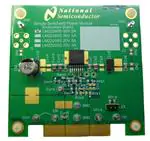
AN-2085 LMZ23605/03, LMZ22005/03 Evaluation Board
1
Introduction
The LMZ23605/03, LMZ22005/03 evaluation boards are designed to be an easy-to-use platform to
evaluate the full capabilities of this family of SIMPLE SWITCHER® power modules. The PCB construction
has excellent thermal performance and includes extra locations for optional components that may not be
required in the end application.
The LMZ23605/03 can accept an input voltage rail between 6V and 36V and the LMZ22005/03 can accept
an input voltage rail between 6V and 20V. The devices can deliver an adjustable and highly accurate
output voltage as low as 0.8V and as high as 6V. The control architecture is constant frequency PWM with
emulated current mode sensing. The control loop operates well with low ESR output capacitors such as
ceramics or specialty polymer. The precision enable input allows for programmable UVLO on the input
supply or flexibility in sequencing. The external soft-start capacitor facilitates controlled output rise time at
startup. The module family is a reliable and robust solution with cycle-by-cycle valley current limit to
protect for over current or short-circuit faults. Additionally there is thermal shutdown protection, and they
will start up into a pre-biased output. The free-running switching frequency is 812 kHz (typ) and a 650 kHz
to 950 kHz synchronization range is supported.
2
Board Specifications
•
•
•
•
•
•
•
•
VIN = 6V to 36V (LMZ22005/03 limited to 20V)
Enable UVLO = 5.7V
VOUT = 3.3V
IOUT = 0 to 5A (LMZ23603 and LMZ22003 limited to 3A)
θJA = 12°C / W, θJC = 1.9°C/W
PCB designed on four layers; Inner are 2 oz; Outer are 3 oz.
Measures 3.5 in. x 3.5 in. (8.9 cm x 8.9 cm) and is 62mil (.062”) thick of FR4 laminate material
Max ambient temp of 70°C at full 5A load (12 Vin)
For additional circuit considerations refer to the Applications Section of the LMZ23605/03 or LMZ22005/03
data sheets. For negative output voltage connections follow the method shown in AN-2027.
All trademarks are the property of their respective owners.
SNVA457B – March 2011 – Revised April 2013
Submit Documentation Feedback
AN-2085 LMZ23605/03, LMZ22005/03 Evaluation Board
Copyright © 2011–2013, Texas Instruments Incorporated
1
�Performance Characteristics
www.ti.com
VOUT
SS/TRK
FB
PGND
AGND
Sync
VIN
EN
VIN
SYNC
LMZ Module
Enable
RSN
VOUT
6V
5V
3.3V
2.5V
1.8V
1.5V
1.2V
1.0V
0.8V
RFBT
15.4k
5.62k
3.32k
2.26k
1.87k
1.00k
1.07k
1.62k
0
RFBB
2.37k
1.07k
1.07k
1.07k
1.50k
1.13k
2.05k
6.49k
8.06k
VIN Range
10...36V
9...36V
7...36V
6...36V
6...36V
6...36V
6...36V
6...36V
6...36V
3.3 VOUT
RENH
100Ö
1.50 kÖ
RFBT 3.32 kÖ
D1
RENT
44.2kÖ
RENB
See table
5.1V
OPT
12.7 kÖ
*
CIN1,2,4,5
2 x 10 PF
+ 2 x 0.047 µF
50V
CIN6
CSS
150 PF
OPT
0.47 PF
CO2
100 PF
X5R
OPT
RFBB
1.07 kÖ
See table
+
CO5
220 PF
6.3V
SP
Figure 1. Evaluation Board Simplified Schematic
3
Performance Characteristics
LMZ23605 3.3Vout Efficiency @ 25°C Ambient
LMZ23605 3.3Vout Dissipation @ 25°C Ambient
100
8
DISSIPATION (W)
EFFICIENCY (%)
90
80
70
60
8 Vin
12 Vin
20 Vin
24 Vin
30 Vin
36 Vin
50
40
0
2
36 Vin
30 Vin
24 Vin
20 Vin
12 Vin
8 Vin
7
1
2
3
4
OUTPUT CURRENT (A)
6
5
4
3
2
1
0
5
0
AN-2085 LMZ23605/03, LMZ22005/03 Evaluation Board
Copyright © 2011–2013, Texas Instruments Incorporated
1
2
3
4
OUTPUT CURRENT (A)
5
SNVA457B – March 2011 – Revised April 2013
Submit Documentation Feedback
�Performance Characteristics
www.ti.com
LMZ23605 3.3Vout Efficiency @ 85°C
LMZ23605 3.3Vout Dissipation @ 85°C
100
8
90
80
70
60
9 Vin
12 Vin
20 Vin
24 Vin
30 Vin
36 Vin
50
40
0
1
2
3
4
OUTPUT CURRENT (A)
6
DISSIPATION (W)
EFFICIENCY (%)
36 Vin
30 Vin
24 Vin
20 Vin
12 Vin
9 Vin
7
5
4
3
2
1
0
5
0
LMZ23605 Load and Line Regulation @ 25°C Ambient
1
2
3
4
OUTPUT CURRENT (A)
5
LMZ23605 Current Limit VOUT = 3.3V
1.002
8
6
CURRENT (A)
OUTPUT VOLTAGE (V)
7
1.001
1.000
9 Vin
12 Vin
20 Vin
24 Vin
30 Vin
36 Vin
0.999
0.998
0
Output Current
5
4
3
2
Input Current
1
1
2
3
4
OUTPUT CURRENT (A)
5
0
0
4
8
12 16 20 24 28 32 36
INPUT VOLTAGE (V)
Output Ripple VOUT = 3.3V
IOUT = 5A, BW to 20 MHz
10 mV/Div
SNVA457B – March 2011 – Revised April 2013
Submit Documentation Feedback
500 ns/Div
Output Ripple VOUT = 3.3V
IOUT = 5A, BW to 250 MHz
10 mV/Div
500 ns/Div
AN-2085 LMZ23605/03, LMZ22005/03 Evaluation Board
Copyright © 2011–2013, Texas Instruments Incorporated
3
�Notes
www.ti.com
LMZ23605 Load Step Response VIN = 12V
VOUT = 3.3V, 0.5A to 5A Step
2A/Div
2A/Div
100 mV/Div
500 µs/Div
LMZ23605 Start-up
4
LMZ23603 Load Step Response VIN = 12V
VOUT = 3.3V, 0.5A to 3A Step
100 mV/Div
500 µs/Div
LMZ23605 Pre-biased startup
Notes
Solder turrets are located on the edge of the PCB assembly for evaluation hookup to bench test
equipment. The Enable input turret is designed for direct connection to the VIN turret. There is a resistive
divider implemented on the board that establishes the 5.5V precision UVLO level of the board. A common
user change to this divider is to raise the value of RENT to increase the operating UVLO to that of the target
application. Refer to the respective data sheet for calculation. Note that if in the end application the
module pin 3 enable voltage does not exceed 5.5V at maximum Vin, then enable clamp zener D1 can be
omitted.
Each implementation of the evaluation board is preset to 3.3V output; with current rating and maximum
input voltage rating dictated by the model of module installed. A common user change is to adjust the
output voltage for different requirements. A table of suggested resistor pairs are listed in Figure 1 for quick
reference.
Locations are provide for testing the operation as a coincident turn-on tracking supply (slave). To
implement this feature, remove CSS and install Rtkt and Rtkb. Calculations are suggested in the respective
data sheets.
A turret is also provided for applying a clock to synchronize the module switching frequency anywhere
between 650 kHz and 950 kHz. Note that a sustained “logic one” on this input corresponds to “zero hertz”
and will cause the module to stop switching.
J1 and J2 are for input and output noise measurement. To implement this feature, populate the 1uF
blocking capacitors and the 49.9 ohm source resistors. Install Amphenol coax connectors type 112404
(Digikey #ACX1051).The added R-C network forms a 2X scope probe when used in conjunction with an
input termination of 50 ohms at the oscilloscope, providing 5 times more sensitivity than a conventional
10x probe.
J3 is for connection to a frequency response analyzer such as A/P Instruments (Ridley) or Venable
Industries products. Refer to the FRA operating manual for this connection. Note: Do not place any type of
shorting jumper to these three posts as that will cause a malfunction.
4
AN-2085 LMZ23605/03, LMZ22005/03 Evaluation Board
Copyright © 2011–2013, Texas Instruments Incorporated
SNVA457B – March 2011 – Revised April 2013
Submit Documentation Feedback
�PCB View and layout diagrams
www.ti.com
Inductor current can be monitored by connecting a loop of between module pin 7 (Vout) and the Co array.
First cut the top side conducting etch between the two vias adjacent to pin 7, then install a 5” loop of 22 ga
insulated wire in the two vias. Monitor the inductor sense loop with an AC/DC oscilloscope current probe.
The Vin input plane has solder mask openings where an input LC network can be placed to accommodate
improved differential mode and conducted EMI performance.
Additional component mounting pads are available to experiment with alternative Cin and Cout
combinations. See Figure 7 for corresponding schematic locations.
5
PCB View and layout diagrams
Gerber and CAD files can be downloaded from the LMZ23605 /03, LMZ22005/03 respective product
folders.
Figure 2. Top View of Assembly
SNVA457B – March 2011 – Revised April 2013
Submit Documentation Feedback
AN-2085 LMZ23605/03, LMZ22005/03 Evaluation Board
Copyright © 2011–2013, Texas Instruments Incorporated
5
�PCB View and layout diagrams
www.ti.com
Figure 3. Top Layer
Figure 4. Internal Layer I (Ground)
Heat Sinking Layer
6
AN-2085 LMZ23605/03, LMZ22005/03 Evaluation Board
Copyright © 2011–2013, Texas Instruments Incorporated
SNVA457B – March 2011 – Revised April 2013
Submit Documentation Feedback
�PCB View and layout diagrams
www.ti.com
Figure 5. Internal Layer II (Ground and Routing)
Heat Sinking Layer
Figure 6. Bottom Layer (Ground)
Heat Sinking Layer
SNVA457B – March 2011 – Revised April 2013
Submit Documentation Feedback
AN-2085 LMZ23605/03, LMZ22005/03 Evaluation Board
Copyright © 2011–2013, Texas Instruments Incorporated
7
�A
8
AN-2085 LMZ23605/03, LMZ22005/03 Evaluation Board
Copyright © 2011–2013, Texas Instruments Incorporated
D1
5.1V
0.2W
Renb
12.7k
Cin2
10 PF
50V
Cin3
10 PF
50V
1.285V Rising Threshold
Cin4
10 PF
50V
DNP
Rsn
1.50k
Cin1
0.047 PF
Renh
100
DNP
Rff
2
J3
DNP
3
2
1
23.7
Rfbb
1.07k
Rfra
Rfbt
DNP
Cff
TT11
3.32k
TT8
CN1
1 PF
50V
DNP
Co1
0.047 PF
Net-Tie
NT1
EN
Vin
GND
GND
GND
GND
Vo
Co2
100 PF
6.3V
GND
GND
Co3
100 PF
6.3V
DNP
TT7
TT10
TT1
TT2
TT3
TT4
TT5
A
B
C
D
E
F
H
J
K
L
NT3
EC1
1
2
3
4
5
6
7
8
9
10
VOUT_S+
TRACK_OPT
SYNC_OPT
VOUT_SVIN_STEMPERATURE
P_GOOD
BIAS_OPT
ENABLE OPT
VIN_S+
NT5
NT2
Co5
220 PF
6.3V
Co6
0.047 PF
CN2
1 PF
50V
DNP
1
J2
DNP
GND
Output Ripple Test Jack
RN2
49.9
DNP
Mates to EDAC 306-010-500-102 Digikey EDC306100
Quick Test Edge Connector V1
VOUT
VOUT
VOUT
GND
GND
GND
GND
VIN
VIN
VIN
Input Ripple Test Jack
2
3
4
5
NT4
Css
0.47 PF
16V
X7R
0805
7
6
5
4
3
2
1
Rent
42.2k
PGND/EP
UVLO@5.5V
TT6
Sync
8
VOUT
SS
FB
AGND
EN
SYNC
VIN
Rtkb
107
DNP
Rtkt
332
DNP
TT9
VTrk
GND
U1
LMZ23605TZ
GND
RTD
100: @ 0- C
Cin6
150 PF
50V
1
J1
DNP
2
3
4
5
GND
Cin5
0.047 PF
RN1
49.9
DNP
PCB View and layout diagrams
www.ti.com
1
DNP = Component not populated
Figure 7. LMZ2360x / LMZ2200x PCB CAD Package Schematic
SNVA457B – March 2011 – Revised April 2013
Submit Documentation Feedback
�PCB View and layout diagrams
www.ti.com
Table 1. Bill of Materials
(1)
(2)
(1) (2)
Designator
Description
Case Size
Manufacturer
Manufacturer P/N
Quantit
y
U1
SIMPLE SWITCHER®
TO-PMOD-7
Texas Instruments
LMZ23605TZ or
LMZ23603TZ or
LMZ22005TZ or
LMZ22003TZ
1
CIN1
CIN5
CO1
CO6
0.047 µF, X7R, 50V
1206
Yageo America
CC1206KRX7R9BB473
4
CIN2
CIN3
10 µF, X5R, 50V
1210
Taiyo Yuden
UMK325BJ106MM-T
2
CIN6 OPT
150 µF,Aluminum
Electrolytic, 50V
G
Panasonic
EEE-FK1H151P
1
CO2 OPT
100 µF, X5R, 6.3V
1210
CO5
220 µF, Specialty
Polymer, 6.3V
TDK
C3225X5R0J107M
1
Panasonic
EEF-UE0J221LR
1
CFF
DNP
CSS
0.47µF, X7R, 16V
0805
AVX
0805YC474KAT2A
1
D1
5.1V 200mW
SOD-323
Diodes Inc.
MMSZ5231BS-7-F
1
RENB
12.7 kΩ
0805
Panasonic
ERJ-6ENF1272V
1
RENT
42.2 kΩ
0805
Panasonic
ERJ-6ENF4222V
1
RENH
100 Ω
0805
Vishay-Dale
CRCW0805100RFKEA
1
RFBT
3.32 kΩ
0805
Vishay-Dale
CRCW08053K32FKEA
1
RFBB
1.07 kΩ
0805
Vishay-Dale
CRCW08051K07FKEA
1
RFRA
23.7 Ω
0805
Vishay-Dale
CRCW080523R7FKEA
1
0805
Vishay-Dale
CRCW08051K50FKEA
1
RFF
DNP
RSN
1.50 kΩ
VIN = 6V to 36V, VOUT = 3.3V, IOUT (MAX) = 5A (3A)
Note: The same BOM applies to all implementations
SNVA457B – March 2011 – Revised April 2013
Submit Documentation Feedback
AN-2085 LMZ23605/03, LMZ22005/03 Evaluation Board
Copyright © 2011–2013, Texas Instruments Incorporated
9
�IMPORTANT NOTICE
Texas Instruments Incorporated and its subsidiaries (TI) reserve the right to make corrections, enhancements, improvements and other
changes to its semiconductor products and services per JESD46, latest issue, and to discontinue any product or service per JESD48, latest
issue. Buyers should obtain the latest relevant information before placing orders and should verify that such information is current and
complete. All semiconductor products (also referred to herein as “components”) are sold subject to TI’s terms and conditions of sale
supplied at the time of order acknowledgment.
TI warrants performance of its components to the specifications applicable at the time of sale, in accordance with the warranty in TI’s terms
and conditions of sale of semiconductor products. Testing and other quality control techniques are used to the extent TI deems necessary
to support this warranty. Except where mandated by applicable law, testing of all parameters of each component is not necessarily
performed.
TI assumes no liability for applications assistance or the design of Buyers’ products. Buyers are responsible for their products and
applications using TI components. To minimize the risks associated with Buyers’ products and applications, Buyers should provide
adequate design and operating safeguards.
TI does not warrant or represent that any license, either express or implied, is granted under any patent right, copyright, mask work right, or
other intellectual property right relating to any combination, machine, or process in which TI components or services are used. Information
published by TI regarding third-party products or services does not constitute a license to use such products or services or a warranty or
endorsement thereof. Use of such information may require a license from a third party under the patents or other intellectual property of the
third party, or a license from TI under the patents or other intellectual property of TI.
Reproduction of significant portions of TI information in TI data books or data sheets is permissible only if reproduction is without alteration
and is accompanied by all associated warranties, conditions, limitations, and notices. TI is not responsible or liable for such altered
documentation. Information of third parties may be subject to additional restrictions.
Resale of TI components or services with statements different from or beyond the parameters stated by TI for that component or service
voids all express and any implied warranties for the associated TI component or service and is an unfair and deceptive business practice.
TI is not responsible or liable for any such statements.
Buyer acknowledges and agrees that it is solely responsible for compliance with all legal, regulatory and safety-related requirements
concerning its products, and any use of TI components in its applications, notwithstanding any applications-related information or support
that may be provided by TI. Buyer represents and agrees that it has all the necessary expertise to create and implement safeguards which
anticipate dangerous consequences of failures, monitor failures and their consequences, lessen the likelihood of failures that might cause
harm and take appropriate remedial actions. Buyer will fully indemnify TI and its representatives against any damages arising out of the use
of any TI components in safety-critical applications.
In some cases, TI components may be promoted specifically to facilitate safety-related applications. With such components, TI’s goal is to
help enable customers to design and create their own end-product solutions that meet applicable functional safety standards and
requirements. Nonetheless, such components are subject to these terms.
No TI components are authorized for use in FDA Class III (or similar life-critical medical equipment) unless authorized officers of the parties
have executed a special agreement specifically governing such use.
Only those TI components which TI has specifically designated as military grade or “enhanced plastic” are designed and intended for use in
military/aerospace applications or environments. Buyer acknowledges and agrees that any military or aerospace use of TI components
which have not been so designated is solely at the Buyer's risk, and that Buyer is solely responsible for compliance with all legal and
regulatory requirements in connection with such use.
TI has specifically designated certain components as meeting ISO/TS16949 requirements, mainly for automotive use. In any case of use of
non-designated products, TI will not be responsible for any failure to meet ISO/TS16949.
Products
Applications
Audio
www.ti.com/audio
Automotive and Transportation
www.ti.com/automotive
Amplifiers
amplifier.ti.com
Communications and Telecom
www.ti.com/communications
Data Converters
dataconverter.ti.com
Computers and Peripherals
www.ti.com/computers
DLP® Products
www.dlp.com
Consumer Electronics
www.ti.com/consumer-apps
DSP
dsp.ti.com
Energy and Lighting
www.ti.com/energy
Clocks and Timers
www.ti.com/clocks
Industrial
www.ti.com/industrial
Interface
interface.ti.com
Medical
www.ti.com/medical
Logic
logic.ti.com
Security
www.ti.com/security
Power Mgmt
power.ti.com
Space, Avionics and Defense
www.ti.com/space-avionics-defense
Microcontrollers
microcontroller.ti.com
Video and Imaging
www.ti.com/video
RFID
www.ti-rfid.com
OMAP Applications Processors
www.ti.com/omap
TI E2E Community
e2e.ti.com
Wireless Connectivity
www.ti.com/wirelessconnectivity
Mailing Address: Texas Instruments, Post Office Box 655303, Dallas, Texas 75265
Copyright © 2013, Texas Instruments Incorporated
�


 工商网监
湘ICP备2023018690号
工商网监
湘ICP备2023018690号