LMZ30604EVM-001, LMZ30604EVM-002, and
LMZ30606EVM-003
User's Guide
Literature Number: SNVU296A
July 2013 – Revised March 2014
�User's Guide
SNVU296A – July 2013 – Revised March 2014
LMZ3060xEVM-00x 2- to 6-A Simple Switcher Power
Module
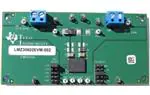
The LMZ30604EVM-001, LMZ30602EVM-002, and LMZ30606 evaluation modules (LMZ3060xEVM-00x)
are designed as an easy-to-use platform that facilitates an extensive evaluation of the features and
performance of the Simple Switcher power module. The EVM PCB may be configured with one of three
devices (see Table 1).
1
Introduction
This user's guide provides information on the correct usage of the EVM and an explanation of the
numerous test points on the board.
Table 1. LMZ3060xEVM-00x Device Configuration
2
DEVICE
TITLE
LMZ30602
2.95 to 6-V input, 2-A output sync, step-down converter with PWM
LMZ30604
2.95 to 6-V input, 4-A output sync, step-down converter with PWM
LMZ30604
2.95 to 6-V input, 6-A output sync, step-down converter with PWM
Description
The EVM features a LMZ3060x synchronous buck power module configured for operation with typical 3.3and 5-V input bus applications. The output voltage can be set to one of five popular values by using a
simple configuration jumper. In similar fashion, the switching frequency can be set to one of four values by
use of a jumper. The full rated output current can be supplied by the EVM. A minimal amount of input and
output capacitance is used on the board. Component pads are provided for additional input and output
capacitors if desired. Monitoring test points are provided to allow measurement of efficiency, power
dissipation, input ripple, output ripple, line and load regulation, and transient response. Control test points
are provided for use of the PWRGD, Inhibit/UVLO, synchronization, and slow-start/tracking features of the
device. The EVM uses a recommended PCB layout that maximizes thermal performance and minimizes
output ripple and noise.
2
LMZ3060xEVM-00x 2- to 6-A Simple Switcher Power Module
Copyright © 2013–2014, Texas Instruments Incorporated
SNVU296A – July 2013 – Revised March 2014
Submit Documentation Feedback
�Getting Started
www.ti.com
3
Getting Started
Figure 1 highlights the user interface items associated with the EVM. The polarized VIN Power terminal
block is used for connection to the host input supply and the polarized VOUT Power terminal block is used
for connection to the load. The terminal blocks can except up to 16 AWG wire.
The VIN monitor and VOUT monitor test points located near the power terminal blocks are intended to be
used as voltage monitoring points where voltmeters can be connected to measure VIN and VOUT. The
voltmeter references should be connected to any of the four VIN/VOUT monitor grounds test points located
between the power terminal blocks. Do not use these VIN and VOUT monitoring test points as the input
supply or output load connection points. The PCB traces connecting to these test points are not designed
to support high currents.
Figure 1. LMZ3060xEVM-00x User Interface
The VIN scope and VOUT scope test points can be used to monitor VIN and VOUT waveforms with an
oscilloscope. These test points are intended for use with un-hooded scope probes. The scope probe tip
should be connected to the socket labeled VIN or VOUT, and the scope ground barrel should lean against
to the test point labeled GND. The GND TP may need to be cut or bent slightly to hold the probe barrel.
Metal Ground Barrel
Probe Tip
TP15
TP16
Figure 2. Tip and Barrel Measurement
The control test points located directly below the LMZ3060x device are made available to test the features
of the device. Any external connections made to these test points should be referenced to either of the
two control ground test points located along the bottom of the EVM. Refer to Section 4 of this user guide
for more information on the individual control test points.
SNVU296A – July 2013 – Revised March 2014
Submit Documentation Feedback
LMZ3060xEVM-00x 2- to 6-A Simple Switcher Power Module
Copyright © 2013–2014, Texas Instruments Incorporated
3
�Test Point Descriptions
www.ti.com
The VOUT-select and FSW-select configuration jumpers are provided for selecting the desired output voltage
and appropriate switching frequency. Before applying power to the EVM, ensure that the jumpers are
present and properly positioned for the intended output voltage. Refer to Table 2 for the recommended
jumper settings. Always remove input power before changing the jumper settings.
Once the jumper settings have been confirmed, configure the host input supply to apply the appropriate
bus voltage listed in Table 2 and confirm that the selected output voltage is obtained.
Table 2. Output Voltage and Switching Frequency Jumper Settings
4
VOUT SELECT
LMZ30602, FSW SELECT
LMZ30604, FSW SELECT
LMZ30606, FSW SELECT
VIN BUS VOLTAGE
3.3 V
1.5 MHz
1 MHz
1 MHz
5V
2.5 V
1.5 MHz
1 MHz
1 MHz
5V
1.8 V
1 MHz
1 MHz
1 MHz
5 V or 3.3 V
1.2 V
750 kHz
750 kHz
750 kHz
5 V or 3.3 V
0.8 V
650 kHz
650 kHz
650 kHz
5 V or 3.3 V
Test Point Descriptions
Fourteen wire-loop test points have been provided as convenient connection points for digital voltmeters
(DVM) or oscilloscope probes to aid in the evaluation of the device. A via labled PH is available near U1 to
scope on the switching frequency. A description of each test point is listed in Table 3
Table 3. Test Point Descriptions
TEST POINT
VIN
Input voltage monitor. Connect DVM to this point for measuring efficiency.
VOUT
Output voltage monitor. Connect DVM to this point for measuring efficiency, line regulation, and load
regulation.
GND
Input and output voltage monitor grounds (located between terminal blocks). Reference the above DVMs
to any of these four ground points.
VIN (scope)
Input voltage scope monitor. Connect an oscilloscope to this set of points to measure input ripple voltage.
VOUT (scope)
Output voltage scope monitor. Connect an oscilloscope to this set of points to measure output ripple
voltage and transient response.
PWRGD
Monitors the power good signal of the device. This is an open drain signal that requires an external pullup resistor to VIN if monitoring is desired. A 10-kΩ to 100-kΩ pullup resistor is recommended. PWRGD is
high if the output voltage is within 92% to 106% of its nominal value.
INH/UVLO
Connect this point to control ground to inhibit the device. Allow this point to float to enable the device. Do
not use a pull-up resistor. An external resistor can be connected from this point to control ground to
increase the under-voltage lockout (UVLO) of the device.
RT/CLK
SS/TR
GND
4
DESCRIPTION
Connects to the RT/CLK pin of the device. An external clock signal can be applied to this point to
synchronize the device to an appropriate frequency.
Connects to the internal slow-start capacitor of the device. An external capacitor can be connected from
this point to control ground to increase the slow-start time of the device. This point can also be used as an
input for tracking applications.
Control grounds (located along bottom of EVM). Reference any signals associated with the control test
points to either of these two ground points.
LMZ3060xEVM-00x 2- to 6-A Simple Switcher Power Module
Copyright © 2013–2014, Texas Instruments Incorporated
SNVU296A – July 2013 – Revised March 2014
Submit Documentation Feedback
�Operation Notes
www.ti.com
5
Operation Notes
The UVLO threshold of the factory-stock EVM is approximately 3.05 V with 0.3 V of hysteresis. The input
voltage must be above the UVLO threshold in order to startup the device. The UVLO threshold can be
increased by adding a resistor to the INH/UVLO test point as described in Table 3. After startup, the
minimum input voltage to the device must be at least 2.95 V or (VOUT + 1.1 V), whichever is greater, in
order to produce a regulated output. The maximum operating input voltage for the device is 6 V. For
further information on the input voltage range and UVLO operation, refer to the device data sheet.
After application of the proper input voltage, the output voltage of the device will ramp to its final value in
approximately 1 ms. If desired, this soft-start time can be increased by adding a capacitor to the SS/TR
test point as described above. Refer to the device datasheet for further information on adjusting the softstart time.
Table 1 lists the recommended switching frequencies for each of the VOUT selections. These
recommendations cover operation over a wide range of input voltage and output load conditions. Several
factors such as duty cycle, minimum on-time, minimum off-time, and current limit influence selection of the
appropriate switching frequency. In some applications, other switching frequencies might be used for
particular output voltages, depending on the above factors. For further information on switching frequency
selection, including synchronization, refer to the device data sheet.
SNVU296A – July 2013 – Revised March 2014
Submit Documentation Feedback
LMZ3060xEVM-00x 2- to 6-A Simple Switcher Power Module
Copyright © 2013–2014, Texas Instruments Incorporated
5
�LMZ3060xEVM-00x Schematic
6
www.ti.com
LMZ3060xEVM-00x Schematic
VIN
TP1
TP14
2
1
VIN
GND
+
TB1
C7
C5
C3
C1
220 μF
0.1 μF
0.1 μF
47 μF
1
U1
LMZ3060xRKG
1
PH
1
3.0 to 5.5 VIN
2
3
SS/TR
4
TP12
5
6
7
1
1
C9
8
C10
0.01 μF
9
0.01 μF
10
11
12
13
RT/CLK
14
15
TP8
16
17
1
R14
113 kΩ
R13
174 kΩ
R7
348 kΩ
R8
715 kΩ
R9
1.2 MΩ
18
R2
100 kΩ
19
J1
2 MHz
1.5 MHz
1 MHz
750 kHz
650 kHz
COMPRTN
VOUT
RC
PGND
COMP
SENSE+
RT/CLK
VADJ
RTRTN
AGND
SS/TR
AGND
STSEL
VIN
VOUT
VIN
VOUT
VIN
VOUT
INHRTN
VOUT
INH/UVLO
VOUT
PWRGD
VOUT
BOOT
VOUT
PH
DNC
PH
DNC
PH
PH
PH
PH
PH
PH
PH
39
38
37
36
35
34
33
R3
2.87 kΩ
32
R4
1.15 kΩ
R5
681 Ω
R6
464 Ω
J2
31
1
2
3
4
5
6
7
8
9
10
1
30
R1
100 kΩ
29
TP10
28
1
R12
100 kΩ
27
R11
100 kΩ
1
26
25
24
3.3
2.5
1.8
1.2
0.8
V
V
V
V
V
Output Select
23
TP11
22
2
21
R10
0Ω
20
PH
1
2
3
4
5
6
7
8
9
10
TP13 TP2
TP7
TB2
C2
47 μF
NOTES:
TP3
TP4
TP5
TP6
C8
C6
+
C4+
1
VOUT
2
220 μF
0.1 μF
1
1
100uF
GND
TP9
1
2
Not Populated
Connect AGND to PGND directly at U1-37 on Layer 1
0.8 to 3.3 VOUT
Figure 3. LMZ3060xEVM-00x Schematic
6
LMZ3060xEVM-00x 2- to 6-A Simple Switcher Power Module
SNVU296A – July 2013 – Revised March 2014
Submit Documentation Feedback
Copyright © 2013–2014, Texas Instruments Incorporated
�PCB Layouts
www.ti.com
7
PCB Layouts
Figure 4. Top Layer
Figure 5. Internal Layer 1
SNVU296A – July 2013 – Revised March 2014
Submit Documentation Feedback
LMZ3060xEVM-00x 2- to 6-A Simple Switcher Power Module
Copyright © 2013–2014, Texas Instruments Incorporated
7
�PCB Layouts
www.ti.com
Figure 6. Internal Layer 2
Figure 7. Bottom Layer
8
LMZ3060xEVM-00x 2- to 6-A Simple Switcher Power Module
Copyright © 2013–2014, Texas Instruments Incorporated
SNVU296A – July 2013 – Revised March 2014
Submit Documentation Feedback
�PCB Layouts
www.ti.com
Figure 8. Top Assembly
Figure 9. Bottom Layer
SNVU296A – July 2013 – Revised March 2014
Submit Documentation Feedback
LMZ3060xEVM-00x 2- to 6-A Simple Switcher Power Module
Copyright © 2013–2014, Texas Instruments Incorporated
9
�Bill of Materials
8
www.ti.com
Bill of Materials
Table 4. LMZ3060xEVM-00x Bill of Materials
-003
-002
-001
REF DES
1
1
1
C1
Capacitor, ceramic, 10 V, x5R, 10%, 47 µF, 1210
GRM32ER61A476K
Murata
1
1
1
C2
Capacitor, ceramic, 6.3 V, x5R, 20%, 47 µF, 1210
GRM32ER60J476M
Murata
1
1
1
C7
Capacitor, polymer, 10 V, 20%, 220 µF, D3L
10TPE220ML
Sanyo
0
0
0
C8
Capacitor, polymer, 10 V, 20%, 220 µF, D3L
10TPE220ML
Sanyo
1
1
1
C4
Capacitor, polymer, 6.3 V, 20%, 100 µF, B2
6TPE100MPB
Sanyo
0
0
0
C3, C5, C6
Capacitor, ceramic, 0.1 µF, 1210
Std
STD
0
0
0
10
Capacitor, ceramic, 0.01 µF, 0402
STD
STD
Part Number
MFR
Header, male 2 x 5 pin, 100-mil spacing, 0.100 inch x 5
PEC05DAAN
inch x 2 inch
Sullins
2
2
2
J1-2
1
1
1
R3
Resistor, chip, 1/16 W, 1%, 2.87 kΩ, 0603
STD
STD
1
1
1
R4
Resistor, chip, 1/16 W, 1%, 1.15 kΩ, 0603
STD
STD
1
1
1
R5
Resistor, chip, 1/16 W, 1%, 681 Ω, 0603
STD
STD
1
1
1
R6
Resistor, chip, 1/16 W, 1%, 464 Ω, 0603
STD
STD
1
1
1
R7
Resistor, chip, 1/16 W, 1%, 348 kΩ, 0603
STD
STD
1
1
1
R8
Resistor, chip, 1/16 W, 1%, 715 kΩ, 0603
STD
STD
1
1
1
R9
Resistor, chip, 1/16 W, 1%, 1.2 MΩ, 0603
STD
STD
1
1
1
R10
Resistor, chip, 1/16 W, 5%, 0 Ω, 0603
STD
STD
1
1
1
R13
Resistor, chip, 1/16 W, 1%, 174 kΩ, 0603
STD
STD
1
1
1
R14
Resistor, chip, 1/16 W, 1%, 113 kΩ, 0603
STD
STD
0
0
0
R1, R2, R11, R12 Resistor, chip, 1/16 W, 1%, 100 kΩ, 0402
Std
Std
ED120/2DS
OST
2
2
2
TB1-2
Terminal block, 2 pin, 15 A, 5.1 mm, 0.40 inch x 0.35
inch
8
8
8
TP1, TP2 TP8
TP10- TP14
Test point, white, thru hole, 5012, 0.125 inch x 0.125
inch
5012
Keystone
6
6
6
TP3-7 TP9
Test point, black, thru hole, 5011, 0.125 inch x 0.125
inch
5011
Keystone
0
0
1
U1
6-V input, 4-A Output Sync. Step-Down Converter with
PWM, QFN
LMZ30604RKG
TI
0
1
0
U1
6-V input, 2-A Output Sync. Step-Down Converter with
PWM, QFN
LMZ30604RKG
TI
1
0
0
U1
6-V input, 6-A Output Sync. Step-Down Converter with
PWM, QFN
LMZ30604RKG
TI
1
1
1
PCB, 0.063 inch H x 1.9 inch L x 3.9 inch W
PWR059
ANY
2
2
2
Conn jumper shorting gold flash
SPC02SYAN
Sullins
4
Bumpon hemisphere 0.44 inch x 0.20 inch clear, 0.440
inch Dia x 0.200 inch H
SJ-5303
3M
4
10
DESCRIPTION
4
LMZ3060xEVM-00x 2- to 6-A Simple Switcher Power Module
Copyright © 2013–2014, Texas Instruments Incorporated
SNVU296A – July 2013 – Revised March 2014
Submit Documentation Feedback
�Revision History
www.ti.com
Revision History
Changes from Original (July 2013) to A Revision ........................................................................................................... Page
•
Updated Figure 3
.........................................................................................................................
6
NOTE: Page numbers for previous revisions may differ from page numbers in the current version.
SNVU296A – July 2013 – Revised March 2014
Submit Documentation Feedback
Revision History
Copyright © 2013–2014, Texas Instruments Incorporated
11
�ADDITIONAL TERMS AND CONDITIONS, WARNINGS, RESTRICTIONS, AND DISCLAIMERS FOR
EVALUATION MODULES
Texas Instruments Incorporated (TI) markets, sells, and loans all evaluation boards, kits, and/or modules (EVMs) pursuant to, and user
expressly acknowledges, represents, and agrees, and takes sole responsibility and risk with respect to, the following:
1.
User agrees and acknowledges that EVMs are intended to be handled and used for feasibility evaluation only in laboratory and/or
development environments. Notwithstanding the foregoing, in certain instances, TI makes certain EVMs available to users that do not
handle and use EVMs solely for feasibility evaluation only in laboratory and/or development environments, but may use EVMs in a
hobbyist environment. All EVMs made available to hobbyist users are FCC certified, as applicable. Hobbyist users acknowledge, agree,
and shall comply with all applicable terms, conditions, warnings, and restrictions in this document and are subject to the disclaimer and
indemnity provisions included in this document.
2. Unless otherwise indicated, EVMs are not finished products and not intended for consumer use. EVMs are intended solely for use by
technically qualified electronics experts who are familiar with the dangers and application risks associated with handling electrical
mechanical components, systems, and subsystems.
3. User agrees that EVMs shall not be used as, or incorporated into, all or any part of a finished product.
4. User agrees and acknowledges that certain EVMs may not be designed or manufactured by TI.
5. User must read the user's guide and all other documentation accompanying EVMs, including without limitation any warning or
restriction notices, prior to handling and/or using EVMs. Such notices contain important safety information related to, for example,
temperatures and voltages. For additional information on TI's environmental and/or safety programs, please visit www.ti.com/esh or
contact TI.
6. User assumes all responsibility, obligation, and any corresponding liability for proper and safe handling and use of EVMs.
7. Should any EVM not meet the specifications indicated in the user’s guide or other documentation accompanying such EVM, the EVM
may be returned to TI within 30 days from the date of delivery for a full refund. THE FOREGOING LIMITED WARRANTY IS THE
EXCLUSIVE WARRANTY MADE BY TI TO USER AND IS IN LIEU OF ALL OTHER WARRANTIES, EXPRESSED, IMPLIED, OR
STATUTORY, INCLUDING ANY WARRANTY OF MERCHANTABILITY OR FITNESS FOR ANY PARTICULAR PURPOSE. TI SHALL
NOT BE LIABLE TO USER FOR ANY INDIRECT, SPECIAL, INCIDENTAL, OR CONSEQUENTIAL DAMAGES RELATED TO THE
HANDLING OR USE OF ANY EVM.
8. No license is granted under any patent right or other intellectual property right of TI covering or relating to any machine, process, or
combination in which EVMs might be or are used. TI currently deals with a variety of customers, and therefore TI’s arrangement with
the user is not exclusive. TI assumes no liability for applications assistance, customer product design, software performance, or
infringement of patents or services with respect to the handling or use of EVMs.
9. User assumes sole responsibility to determine whether EVMs may be subject to any applicable federal, state, or local laws and
regulatory requirements (including but not limited to U.S. Food and Drug Administration regulations, if applicable) related to its handling
and use of EVMs and, if applicable, compliance in all respects with such laws and regulations.
10. User has sole responsibility to ensure the safety of any activities to be conducted by it and its employees, affiliates, contractors or
designees, with respect to handling and using EVMs. Further, user is responsible to ensure that any interfaces (electronic and/or
mechanical) between EVMs and any human body are designed with suitable isolation and means to safely limit accessible leakage
currents to minimize the risk of electrical shock hazard.
11. User shall employ reasonable safeguards to ensure that user’s use of EVMs will not result in any property damage, injury or death,
even if EVMs should fail to perform as described or expected.
12. User shall be solely responsible for proper disposal and recycling of EVMs consistent with all applicable federal, state, and local
requirements.
Certain Instructions. User shall operate EVMs within TI’s recommended specifications and environmental considerations per the user’s
guide, accompanying documentation, and any other applicable requirements. Exceeding the specified ratings (including but not limited to
input and output voltage, current, power, and environmental ranges) for EVMs may cause property damage, personal injury or death. If
there are questions concerning these ratings, user should contact a TI field representative prior to connecting interface electronics including
input power and intended loads. Any loads applied outside of the specified output range may result in unintended and/or inaccurate
operation and/or possible permanent damage to the EVM and/or interface electronics. Please consult the applicable EVM user's guide prior
to connecting any load to the EVM output. If there is uncertainty as to the load specification, please contact a TI field representative. During
normal operation, some circuit components may have case temperatures greater than 60°C as long as the input and output are maintained
at a normal ambient operating temperature. These components include but are not limited to linear regulators, switching transistors, pass
transistors, and current sense resistors which can be identified using EVMs’ schematics located in the applicable EVM user's guide. When
placing measurement probes near EVMs during normal operation, please be aware that EVMs may become very warm. As with all
electronic evaluation tools, only qualified personnel knowledgeable in electronic measurement and diagnostics normally found in
development environments should use EVMs.
Agreement to Defend, Indemnify and Hold Harmless. User agrees to defend, indemnify, and hold TI, its directors, officers, employees,
agents, representatives, affiliates, licensors and their representatives harmless from and against any and all claims, damages, losses,
expenses, costs and liabilities (collectively, "Claims") arising out of, or in connection with, any handling and/or use of EVMs. User’s
indemnity shall apply whether Claims arise under law of tort or contract or any other legal theory, and even if EVMs fail to perform as
described or expected.
Safety-Critical or Life-Critical Applications. If user intends to use EVMs in evaluations of safety critical applications (such as life support),
and a failure of a TI product considered for purchase by user for use in user’s product would reasonably be expected to cause severe
personal injury or death such as devices which are classified as FDA Class III or similar classification, then user must specifically notify TI
of such intent and enter into a separate Assurance and Indemnity Agreement.
�RADIO FREQUENCY REGULATORY COMPLIANCE INFORMATION FOR EVALUATION MODULES
Texas Instruments Incorporated (TI) evaluation boards, kits, and/or modules (EVMs) and/or accompanying hardware that is marketed, sold,
or loaned to users may or may not be subject to radio frequency regulations in specific countries.
General Statement for EVMs Not Including a Radio
For EVMs not including a radio and not subject to the U.S. Federal Communications Commission (FCC) or Industry Canada (IC)
regulations, TI intends EVMs to be used only for engineering development, demonstration, or evaluation purposes. EVMs are not finished
products typically fit for general consumer use. EVMs may nonetheless generate, use, or radiate radio frequency energy, but have not been
tested for compliance with the limits of computing devices pursuant to part 15 of FCC or the ICES-003 rules. Operation of such EVMs may
cause interference with radio communications, in which case the user at his own expense will be required to take whatever measures may
be required to correct this interference.
General Statement for EVMs including a radio
User Power/Frequency Use Obligations: For EVMs including a radio, the radio included in such EVMs is intended for development and/or
professional use only in legally allocated frequency and power limits. Any use of radio frequencies and/or power availability in such EVMs
and their development application(s) must comply with local laws governing radio spectrum allocation and power limits for such EVMs. It is
the user’s sole responsibility to only operate this radio in legally acceptable frequency space and within legally mandated power limitations.
Any exceptions to this are strictly prohibited and unauthorized by TI unless user has obtained appropriate experimental and/or development
licenses from local regulatory authorities, which is the sole responsibility of the user, including its acceptable authorization.
U.S. Federal Communications Commission Compliance
For EVMs Annotated as FCC – FEDERAL COMMUNICATIONS COMMISSION Part 15 Compliant
Caution
This device complies with part 15 of the FCC Rules. Operation is subject to the following two conditions: (1) This device may not cause
harmful interference, and (2) this device must accept any interference received, including interference that may cause undesired operation.
Changes or modifications could void the user's authority to operate the equipment.
FCC Interference Statement for Class A EVM devices
This equipment has been tested and found to comply with the limits for a Class A digital device, pursuant to part 15 of the FCC Rules.
These limits are designed to provide reasonable protection against harmful interference when the equipment is operated in a commercial
environment. This equipment generates, uses, and can radiate radio frequency energy and, if not installed and used in accordance with the
instruction manual, may cause harmful interference to radio communications. Operation of this equipment in a residential area is likely to
cause harmful interference in which case the user will be required to correct the interference at its own expense.
FCC Interference Statement for Class B EVM devices
This equipment has been tested and found to comply with the limits for a Class B digital device, pursuant to part 15 of the FCC Rules.
These limits are designed to provide reasonable protection against harmful interference in a residential installation. This equipment
generates, uses and can radiate radio frequency energy and, if not installed and used in accordance with the instructions, may cause
harmful interference to radio communications. However, there is no guarantee that interference will not occur in a particular installation. If
this equipment does cause harmful interference to radio or television reception, which can be determined by turning the equipment off and
on, the user is encouraged to try to correct the interference by one or more of the following measures:
• Reorient or relocate the receiving antenna.
• Increase the separation between the equipment and receiver.
• Connect the equipment into an outlet on a circuit different from that to which the receiver is connected.
• Consult the dealer or an experienced radio/TV technician for help.
Industry Canada Compliance (English)
For EVMs Annotated as IC – INDUSTRY CANADA Compliant:
This Class A or B digital apparatus complies with Canadian ICES-003.
Changes or modifications not expressly approved by the party responsible for compliance could void the user’s authority to operate the
equipment.
Concerning EVMs Including Radio Transmitters
This device complies with Industry Canada licence-exempt RSS standard(s). Operation is subject to the following two conditions: (1) this
device may not cause interference, and (2) this device must accept any interference, including interference that may cause undesired
operation of the device.
Concerning EVMs Including Detachable Antennas
Under Industry Canada regulations, this radio transmitter may only operate using an antenna of a type and maximum (or lesser) gain
approved for the transmitter by Industry Canada. To reduce potential radio interference to other users, the antenna type and its gain should
be so chosen that the equivalent isotropically radiated power (e.i.r.p.) is not more than that necessary for successful communication.
This radio transmitter has been approved by Industry Canada to operate with the antenna types listed in the user guide with the maximum
permissible gain and required antenna impedance for each antenna type indicated. Antenna types not included in this list, having a gain
greater than the maximum gain indicated for that type, are strictly prohibited for use with this device.
�Canada Industry Canada Compliance (French)
Cet appareil numérique de la classe A ou B est conforme à la norme NMB-003 du Canada
Les changements ou les modifications pas expressément approuvés par la partie responsable de la conformité ont pu vider l’autorité de
l'utilisateur pour actionner l'équipement.
Concernant les EVMs avec appareils radio
Le présent appareil est conforme aux CNR d'Industrie Canada applicables aux appareils radio exempts de licence. L'exploitation est
autorisée aux deux conditions suivantes : (1) l'appareil ne doit pas produire de brouillage, et (2) l'utilisateur de l'appareil doit accepter tout
brouillage radioélectrique subi, même si le brouillage est susceptible d'en compromettre le fonctionnement.
Concernant les EVMs avec antennes détachables
Conformément à la réglementation d'Industrie Canada, le présent émetteur radio peut fonctionner avec une antenne d'un type et d'un gain
maximal (ou inférieur) approuvé pour l'émetteur par Industrie Canada. Dans le but de réduire les risques de brouillage radioélectrique à
l'intention des autres utilisateurs, il faut choisir le type d'antenne et son gain de sorte que la puissance isotrope rayonnée équivalente
(p.i.r.e.) ne dépasse pas l'intensité nécessaire à l'établissement d'une communication satisfaisante.
Le présent émetteur radio a été approuvé par Industrie Canada pour fonctionner avec les types d'antenne énumérés dans le manuel
d’usage et ayant un gain admissible maximal et l'impédance requise pour chaque type d'antenne. Les types d'antenne non inclus dans
cette liste, ou dont le gain est supérieur au gain maximal indiqué, sont strictement interdits pour l'exploitation de l'émetteur.
Mailing Address: Texas Instruments, Post Office Box 655303, Dallas, Texas 75265
Copyright © 2014, Texas Instruments Incorporated
spacer
Important Notice for Users of EVMs Considered “Radio Frequency Products” in Japan
EVMs entering Japan are NOT certified by TI as conforming to Technical Regulations of Radio Law of Japan.
If user uses EVMs in Japan, user is required by Radio Law of Japan to follow the instructions below with respect to EVMs:
1.
2.
3.
Use EVMs in a shielded room or any other test facility as defined in the notification #173 issued by Ministry of Internal Affairs and
Communications on March 28, 2006, based on Sub-section 1.1 of Article 6 of the Ministry’s Rule for Enforcement of Radio Law of
Japan,
Use EVMs only after user obtains the license of Test Radio Station as provided in Radio Law of Japan with respect to EVMs, or
Use of EVMs only after user obtains the Technical Regulations Conformity Certification as provided in Radio Law of Japan with respect
to EVMs. Also, do not transfer EVMs, unless user gives the same notice above to the transferee. Please note that if user does not
follow the instructions above, user will be subject to penalties of Radio Law of Japan.
http://www.tij.co.jp
【無線電波を送信する製品の開発キットをお使いになる際の注意事項】 本開発キットは技術基準適合証明を受けておりません。 本製品の
ご使用に際しては、電波法遵守のため、以下のいずれかの措置を取っていただく必要がありますのでご注意ください。
1.
2.
3.
電波法施行規則第6条第1項第1号に基づく平成18年3月28日総務省告示第173号で定められた電波暗室等の試験設備でご使用いただく。
実験局の免許を取得後ご使用いただく。
技術基準適合証明を取得後ご使用いただく。。
なお、本製品は、上記の「ご使用にあたっての注意」を譲渡先、移転先に通知しない限り、譲渡、移転できないものとします
上記を遵守頂けない場合は、電波法の罰則が適用される可能性があることをご留意ください。
日本テキサス・インスツルメンツ株式会社
東京都新宿区西新宿6丁目24番1号
西新宿三井ビル
http://www.tij.co.jp
Texas Instruments Japan Limited
(address) 24-1, Nishi-Shinjuku 6 chome, Shinjuku-ku, Tokyo, Japan
�IMPORTANT NOTICE
Texas Instruments Incorporated and its subsidiaries (TI) reserve the right to make corrections, enhancements, improvements and other
changes to its semiconductor products and services per JESD46, latest issue, and to discontinue any product or service per JESD48, latest
issue. Buyers should obtain the latest relevant information before placing orders and should verify that such information is current and
complete. All semiconductor products (also referred to herein as “components”) are sold subject to TI’s terms and conditions of sale
supplied at the time of order acknowledgment.
TI warrants performance of its components to the specifications applicable at the time of sale, in accordance with the warranty in TI’s terms
and conditions of sale of semiconductor products. Testing and other quality control techniques are used to the extent TI deems necessary
to support this warranty. Except where mandated by applicable law, testing of all parameters of each component is not necessarily
performed.
TI assumes no liability for applications assistance or the design of Buyers’ products. Buyers are responsible for their products and
applications using TI components. To minimize the risks associated with Buyers’ products and applications, Buyers should provide
adequate design and operating safeguards.
TI does not warrant or represent that any license, either express or implied, is granted under any patent right, copyright, mask work right, or
other intellectual property right relating to any combination, machine, or process in which TI components or services are used. Information
published by TI regarding third-party products or services does not constitute a license to use such products or services or a warranty or
endorsement thereof. Use of such information may require a license from a third party under the patents or other intellectual property of the
third party, or a license from TI under the patents or other intellectual property of TI.
Reproduction of significant portions of TI information in TI data books or data sheets is permissible only if reproduction is without alteration
and is accompanied by all associated warranties, conditions, limitations, and notices. TI is not responsible or liable for such altered
documentation. Information of third parties may be subject to additional restrictions.
Resale of TI components or services with statements different from or beyond the parameters stated by TI for that component or service
voids all express and any implied warranties for the associated TI component or service and is an unfair and deceptive business practice.
TI is not responsible or liable for any such statements.
Buyer acknowledges and agrees that it is solely responsible for compliance with all legal, regulatory and safety-related requirements
concerning its products, and any use of TI components in its applications, notwithstanding any applications-related information or support
that may be provided by TI. Buyer represents and agrees that it has all the necessary expertise to create and implement safeguards which
anticipate dangerous consequences of failures, monitor failures and their consequences, lessen the likelihood of failures that might cause
harm and take appropriate remedial actions. Buyer will fully indemnify TI and its representatives against any damages arising out of the use
of any TI components in safety-critical applications.
In some cases, TI components may be promoted specifically to facilitate safety-related applications. With such components, TI’s goal is to
help enable customers to design and create their own end-product solutions that meet applicable functional safety standards and
requirements. Nonetheless, such components are subject to these terms.
No TI components are authorized for use in FDA Class III (or similar life-critical medical equipment) unless authorized officers of the parties
have executed a special agreement specifically governing such use.
Only those TI components which TI has specifically designated as military grade or “enhanced plastic” are designed and intended for use in
military/aerospace applications or environments. Buyer acknowledges and agrees that any military or aerospace use of TI components
which have not been so designated is solely at the Buyer's risk, and that Buyer is solely responsible for compliance with all legal and
regulatory requirements in connection with such use.
TI has specifically designated certain components as meeting ISO/TS16949 requirements, mainly for automotive use. In any case of use of
non-designated products, TI will not be responsible for any failure to meet ISO/TS16949.
Products
Applications
Audio
www.ti.com/audio
Automotive and Transportation
www.ti.com/automotive
Amplifiers
amplifier.ti.com
Communications and Telecom
www.ti.com/communications
Data Converters
dataconverter.ti.com
Computers and Peripherals
www.ti.com/computers
DLP® Products
www.dlp.com
Consumer Electronics
www.ti.com/consumer-apps
DSP
dsp.ti.com
Energy and Lighting
www.ti.com/energy
Clocks and Timers
www.ti.com/clocks
Industrial
www.ti.com/industrial
Interface
interface.ti.com
Medical
www.ti.com/medical
Logic
logic.ti.com
Security
www.ti.com/security
Power Mgmt
power.ti.com
Space, Avionics and Defense
www.ti.com/space-avionics-defense
Microcontrollers
microcontroller.ti.com
Video and Imaging
www.ti.com/video
RFID
www.ti-rfid.com
OMAP Applications Processors
www.ti.com/omap
TI E2E Community
e2e.ti.com
Wireless Connectivity
www.ti.com/wirelessconnectivity
Mailing Address: Texas Instruments, Post Office Box 655303, Dallas, Texas 75265
Copyright © 2014, Texas Instruments Incorporated
�