www.ti.com
Table of Contents
User’s Guide
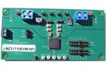
LMZ3170x Power Module Evaluation Module User's Guide
ABSTRACT
The LMZ31710EVM-001, LMZ31707EVM-002, and LMZ31704EVM-003 evaluation modules are designed as an
easy-to-use platform that facilitates an extensive evaluation of the features and performance of the SIMPLE
SWITCHER® power module. This guide provides information on the correct usage of the EVM and an
explanation of the numerous test points on the board.
Table of Contents
1 Description.............................................................................................................................................................................. 2
2 Getting Started........................................................................................................................................................................2
3 Test Point Descriptions.......................................................................................................................................................... 4
4 Operation Notes......................................................................................................................................................................5
5 Performance Data................................................................................................................................................................... 6
6 Schematic................................................................................................................................................................................8
7 Bill of Materials....................................................................................................................................................................... 9
8 PCB Layout............................................................................................................................................................................11
9 Revision History................................................................................................................................................................... 13
List of Figures
Figure 2-1. LMZ317xxEVM User Interface.................................................................................................................................. 2
Figure 5-1. LMZ31710EVM Efficiency......................................................................................................................................... 6
Figure 5-2. LMZ31710EVM Power Dissipation............................................................................................................................6
Figure 5-3. LMZ31710EVM Load Regulation.............................................................................................................................. 6
Figure 5-4. LMZ31710EVM Line Regulation............................................................................................................................... 6
Figure 5-5. LMZ31710EVM Output Ripple.................................................................................................................................. 6
Figure 5-6. LMZ31710EVM Output Ripple Waveforms............................................................................................................... 6
Figure 5-7. LMZ31710EVM Transient Response Waveforms..................................................................................................... 7
Figure 5-8. LMZ31710EVM Start-Up Waveforms........................................................................................................................ 7
Figure 6-1. LMZ317xxEVM Schematic........................................................................................................................................ 8
Figure 8-1. LMZ317xxEVM Topside Component Layout........................................................................................................... 11
Figure 8-2. LMZ317xxEVM Bottom-Side Component Layout.................................................................................................... 11
Figure 8-3. LMZ317xxEVM Layer 1 Copper.............................................................................................................................. 12
Figure 8-4. LMZ317xxEVM Layer 2 Copper.............................................................................................................................. 12
Figure 8-5. LMZ317xxEVM Layer 3 Copper.............................................................................................................................. 13
Figure 8-6. LMZ317xxEVM Layer 4 Copper.............................................................................................................................. 13
List of Tables
Table 2-1. Output Voltage and Switching Frequency Jumper Settings........................................................................................3
Table 3-1. Test Point Descriptions(1) ........................................................................................................................................... 4
Table 7-1. LMZ317xxEVM Bill of Materials.................................................................................................................................. 9
Trademarks
SIMPLE SWITCHER® is a registered trademark of Texas Instruments.
All trademarks are the property of their respective owners.
SLVU895B – MARCH 2013 – REVISED JANUARY 2022
LMZ3170x Power Module Evaluation Module User's Guide
Submit Document Feedback
Copyright © 2022 Texas Instruments Incorporated
1
�Description
www.ti.com
1 Description
This EVM features the LMZ31710 (10-A), LMZ31707 (7-A), or LMZ31704 (4-A) synchronous buck power module
configured for operation with typical 5-V and 12-V input bus applications. The output voltage can be set to one
of seven popular values by using a configuration jumper. In similar fashion, the switching frequency can be set to
one of seven values with a jumper. The full output current rating of the device can be supplied by the EVM. Input
and output capacitors are included on the board to accommodate the entire range of input and output voltages.
Monitoring test points are provided to allow measurement of the following:
•
•
•
•
•
•
Efficiency
Power dissipation
Input ripple
Output ripple
Line and load regulation
Transient response
Control test points are provided for use of the PWRGD, inhibit/UVLO, synchronization, and slow-start/tracking
features of the LMZ317xx device. The EVM uses a recommended PCB layout that maximizes thermal
performance and minimizes output ripple and noise.
2 Getting Started
Figure 2-1 highlights the user interface items associated with the EVM. The polarized PVin Power terminal block
(TB1) is used for connection to the host input supply and the polarized Vout Power terminal block (TB2) is used
for connection to the load. These terminal blocks can accept up to 16-AWG wire. The polarized Vbias terminal
block (TB3) is used along with the VIN select jumper (P1) when optional split power supply operation is desired.
Refer to the LMZ317xx data sheets (LMZ31710 10-A Module, 2.95-V to 17-V Input and Current Sharing in QFN
Package Data Sheet, LMZ31707 7-A Power Module with 2.95-V to 17-V Input Current Sharing in QFN Data
Sheet, and LMZ31704 4-A Power Module with 2.95-V to 17-V Input and Current Sharing Data Sheet) for further
information on split power supply operation.
Figure 2-1. LMZ317xxEVM User Interface
The PVin Monitor and Vout Monitor test points located near the power terminal blocks are intended to be used
as voltage monitoring points where voltmeters can be connected to measure PVin and Vout. The voltmeter
references should be connected to any of the four PVin/Vout Monitor Grounds test points located between the
power terminal blocks. Do not use these PVin and Vout monitoring test points as the input supply or output load
connection points. The PCB traces connecting to these test points are not designed to support high currents.
2
LMZ3170x Power Module Evaluation Module User's Guide
SLVU895B – MARCH 2013 – REVISED JANUARY 2022
Submit Document Feedback
Copyright © 2022 Texas Instruments Incorporated
�www.ti.com
Getting Started
The PVin Scope and Vout Scope test points can be used to monitor PVin and Vout waveforms with an
oscilloscope. These test points are intended for use with un-hooded scope probes outfitted with a low-inductance
ground lead (ground spring) mounted to the scope barrel. The two sockets of each test point are on 0.1 in
centers. The scope probe tip should be connected to the socket labeled PVin or Vout, and the scope ground lead
should be connected to the socket labeled PGND.
The Controls test points located directly below the device are made available to test the features of the device.
Any external connections made to these test points should be referenced to the Control Ground test point
located along the bottom of the EVM. Refer to Section 3 for more information on the individual control test points.
The Vout Select jumper (P3) and Fsw Select jumper (P2) are provided for selecting the desired output voltage
and appropriate switching frequency. Before applying power to the EVM, ensure that the jumpers are present
and properly positioned for the intended output voltage. Refer to Table 2-1 for the recommended jumper settings.
Always remove input power before changing the jumper settings.
Once the jumper settings have been confirmed, configure the host input supply to apply the appropriate bus
voltage listed in Table 2-1 and confirm that the selected output voltage is obtained.
Table 2-1. Output Voltage and Switching Frequency Jumper Settings
VOUT Select
FSW Select
PVin Bus Voltage
5.0 V
1 MHz
12 V
3.3 V
750 kHz
5 V or 12 V
2.5 V
750 kHz
5 V or 12 V
1.8 V
500 kHz
5 V or 12 V
1.2 V
300 kHz
5 V or 12 V
0.9 V
250 kHz
5 V or 12 V
0.6 V
200 kHz
5 V or 12 V
SLVU895B – MARCH 2013 – REVISED JANUARY 2022
LMZ3170x Power Module Evaluation Module User's Guide
Submit Document Feedback
Copyright © 2022 Texas Instruments Incorporated
3
�Test Point Descriptions
www.ti.com
3 Test Point Descriptions
Twelve wire-loop test points and two scope probe test points have been provided as convenient connection
points for digital voltmeters (DVM) or oscilloscope probes to aid in the evaluation of the device. A description of
each test point follows:
Table 3-1. Test Point Descriptions(1)
Test Point
Description
PVIN
Input voltage monitor. Connect DVM to this point to measure efficiency.
VOUT
Output voltage monitor. Connect DVM to this point to measure efficiency, line regulation, and load
regulation.
AGND
Input and output voltage monitor grounds (located between terminal blocks). Reference the above
DVMs to any of these four analog ground points.
PVIN Scope (J1)
Input voltage scope monitor. Connect an oscilloscope to this set of points to measure input ripple
voltage.
VOUT Scope (J2)
Output voltage scope monitor. Connect an oscilloscope to this set of points to measure output ripple
voltage and transient response.
PWRGD
Monitors the power-good signal of the device. This is an open-drain signal that requires an external
pullup resistor if monitoring is desired. A 10-kΩ to 100-kΩ pullup resistor is recommended. PWRGD
is high if the output voltage is within 92% to 107% of its nominal value.
INH/UVLO
Connect this point to control ground to inhibit the device. Allow this point to float to enable the
device. An external resistor divider can be connected between this point, control ground, and VIN to
adjust the UVLO of the device.
RT/CLK
Connects to the RT/CLK pin of the device. An external clock signal can be applied to this point to
synchronize the device to an appropriate frequency.
SS/TR
Connects to the internal slow-start capacitor of the device. An external capacitor can be connected
from this point to control ground to increase the slow-start time of the device. This point can also be
used to track applications.
SYNC_OUT
This output provides a clock signal that is 180° out of phase with the PH node of the device and can
be used to synchronize other devices.
AGND
Control ground (located along bottom of EVM). Reference any signals associated with the control
test points to this analog ground point.
(1)
4
Refer to the LMZ317xx data sheets for absolute maximum ratings associated with these features.
LMZ3170x Power Module Evaluation Module User's Guide
SLVU895B – MARCH 2013 – REVISED JANUARY 2022
Submit Document Feedback
Copyright © 2022 Texas Instruments Incorporated
�www.ti.com
Operation Notes
4 Operation Notes
In order to operate the EVM using a single power supply, the Vin Select jumper (P1) must be in the default
PVIN-VIN position shown in Figure 2-1. In this position, the PVin and Vin pins of the device are connected
together. The UVLO threshold of the EVM is approximately 4 V with 0.15 V of hysteresis. The input voltage must
be above the UVLO threshold in order for the device to start-up. After start-up, the minimum input voltage to the
device must be at least 4.5 V or (VOUT + 0.7 V), whichever is greater. The maximum operating input voltage for
the device is 17 V. Refer to the LMZ317xx data sheets for further information on the input voltage range, UVLO
operation, and optional split power supply operation for operating with PVin as low as 2.95 V when using an
external Vbias supply.
After application of the proper input voltage, the output voltage of the device will ramp to its final value in
approximately 1.2 ms. If desired, this soft-start time can be increased by adding a capacitor to the SS/TR test
point as described above. Refer to the LMZ317xx data sheets for further information on adjusting the soft-start
time.
Table 2-1 lists the recommended switching frequencies for each of the VOUT selections. These
recommendations cover operation over a wide range of input voltage and output load conditions. Several
factors such as duty cycle, minimum on-time, minimum off-time, and current limit influence selection of the
appropriate switching frequency. In some applications, other switching frequencies can be used for particular
output voltages, depending on the above factors. Refer to the LMZ317xx data sheets for further information on
switching frequency selection, including synchronization.
The EVM includes input and output capacitors to accommodate the entire range of input and output voltage
conditions. The actual capacitance required will depend on the input and output voltage conditions of the
particular application, along with the desired transient response. In most cases, the required output capacitance
will be less than that supplied on the EVM. Refer to the LMZ317xx data sheets for further information on the
minimum required I/O capacitance and transient response.
The LMZ317xx operates in pulse skip mode at light currents to improve light load efficiency (LLE mode). At
output voltages of less than 1.5 V, the pulse skipping can cause the output to rise when there is no load to
discharge the energy. A minimum load of 600 µA or less, depending on VOUT, is required to keep the output
voltage within regulation. For the worst case condition of VOUT = 0.6 V, a 1-kΩ resistor would provide a required
minimum load of 600 µA. If the application requires an additional load to meet the minimum load requirement,
the additional load can be connected external to the EVM or installed in the R16 position on the underside of
the EVM. Refer to the LMZ317xx data sheets for further information on LLE mode and determining the required
minimum load.
SLVU895B – MARCH 2013 – REVISED JANUARY 2022
LMZ3170x Power Module Evaluation Module User's Guide
Submit Document Feedback
Copyright © 2022 Texas Instruments Incorporated
5
�Performance Data
www.ti.com
5 Performance Data
Figure 5-1 through Figure 5-8 demonstrate the LMZ31710EVM performance with VOUT = 1.8 V and
FSW = 500 kHz. For data regarding the LMZ31707 and the LMZ31704, please see the product data sheet.
3.5
100
90
VOUT = 1.8 V
FSW = 500 kHz
3.0
70
2.5
60
2.0
PDISS (W)
Efficiency (%)
80
50
40
30
20
0
PVIN _VIN
1.0
PVIN _VIN
5V
12 V
0.5
5V
12 V
VOUT = 1.8 V
FSW = 500 kHz
10
0
1
2
3
4
5
6
Iout (A)
7
1.5
8
9
0
10
Figure 5-1. LMZ31710EVM Efficiency
0
1
2
3
4
5
6
IOUT (A)
7
8
9
10
Figure 5-2. LMZ31710EVM Power Dissipation
1.828
1.828
VOUT = 1.8 V
FSW = 500 kHz
1.820
VOUT = 1.8 V
FSW = 500 kHz
1.820
1.812
VOUT (V)
1.812
1.804
VOUT (V)
1.804
1.796
1.796
IOUT
1.788
PVIN _VIN
1.788
1.780
5V
12 V
1.780
1.772
0
1
2
3
4
5
6
IOUT (A)
7
8
9
10
Figure 5-3. LMZ31710EVM Load Regulation
1.772
0A
5A
10 A
5
7
9
11
PVIN_VIN (V)
13
15
17
Figure 5-4. LMZ31710EVM Line Regulation
0.030
VOUT = 1.8 V
FSW = 500 kHz
Output Ripple (V-pk-pk)
0.025
VOUT
10 mV/div
0.020
0.015
0.010
VOUT
10 mV/div
PVIN _VIN
0.005
0.000
fSW = 500 kHz
IOUT = 10 A
VOUT = 1.8 V
PVIN = 12 V
5V
12 V
0
1
2
3
4
5
6
IOUT (A)
7
8
9
Figure 5-5. LMZ31710EVM Output Ripple
6
PVIN = 5 V
LMZ3170x Power Module Evaluation Module User's Guide
10
1 µs/div
Figure 5-6. LMZ31710EVM Output Ripple
Waveforms
SLVU895B – MARCH 2013 – REVISED JANUARY 2022
Submit Document Feedback
Copyright © 2022 Texas Instruments Incorporated
�www.ti.com
Performance Data
VOUT
100 mV/div
PVIN = 5 V
PVIN = 5 V/div
fSW = 500 kHz
IOUT = 10 A
VOUT = 1.8 V
VOUT 1 V/div
VOUT
100 mV/div
PVIN = 12 V
fSW = 500 kHz
IOUT = 10 A
VOUT = 1.8 V
PVIN = 12 V
SS/TR 1 V/div
200 µs/div
Figure 5-7. LMZ31710EVM Transient Response
Waveforms
2 ms/div
Figure 5-8. LMZ31710EVM Start-Up Waveforms
SLVU895B – MARCH 2013 – REVISED JANUARY 2022
LMZ3170x Power Module Evaluation Module User's Guide
Submit Document Feedback
Copyright © 2022 Texas Instruments Incorporated
7
�TB1
NOTES:
See Table in BOM for part number.
C10
4.7µF
25V
2
3
C7
100µF
25V
Not Populated.
RT/CLK
1
2
+
1
TP8
RT/CLK
SYNC_OUT
AGND
TP9
AGND
TP7
SYNC_OUT
PWRGD
PGND
VBIAS
P1
PGND
PVIN
PVIN
VIN
VBIAS
TP11
PWRGD
4.5V to 17V
PGND
VBIAS
TB3
PGND
2.95V to 17V
PVIN
PGND
1
TP1
PVIN
PVIN
PGND
PGND
J1
C5
22µF
25V
C9
0.1µF
25V
C1
22µF
25V
FREQUENCY
SELECT
P2
TP14
AGND
1
2
3
4
5
6
7
8
9
10
11
12
13
14
200kHz
250kHz
300kHz
500kHz
750kHz
1.0MHz
1.2MHz
R3
52.3k
1
1
AGND
VIN
DNC
DNC
ILIM
SYNC_OUT
PWRGD
DNC
PH
TP12
PHASE
2
3
4
5
6
7
8
9
10
PGND
AGND
C3
22µF
25V
1
40
39
12
11
41
38
37
36
35
34
33
32
31
21
20
2
U1
PH
PH
PH
PH
PH
PH
PH
PH
LMZ3170x Power Module Evaluation Module User's Guide
R4
63.4k
R5
90.9k
R6
169k
13
14
15
16
17
18
19
42
8
R15
R7
487k
PGND
1
C2
100µF
6.3V
INH/UVLO
STSEL
SS/TR
SENSE+
VADJ
ISHARE
DNC
AGND
RT/CLK
PVIN
PVIN
PVIN
PVIN
PVIN
VOUT
VOUT
VOUT
VOUT
VOUT
VOUT
PGND
PGND
PGND
PGND
PGND
P4
R8
1M
30
29
28
27
26
25
24
23
22
R9
2.87k
C4
100µF
6.3V
R10
1.43k
1
R2
C6
100µF
6.3V
VOUT
R11
715 Ω
1
R1
PGND
+
R12
453 Ω
J2
R13
316 Ω
C8
220µF
10V
R14
196 Ω
1
R16
SS/TR
INH/UVLO
TB2
P5
VOUT
PGND
1
0.6V
0.9V
1.2V
1.8V
2.5V
3.3V
5.0V
1
2
3
4
5
6
7
8
9
10
11
12
13
14
P3
VOUT
SELECT
TP6
TP5 AGND
TP4
TP3
TP13
SS/TR
TP10
INH/UVLO
0.6V to 5.5V / 10A
AGND
PGND
VOUT
TP2
VOUT
Schematic
www.ti.com
6 Schematic
Figure 6-1 is the schematic for this EVM.
Figure 6-1. LMZ317xxEVM Schematic
SLVU895B – MARCH 2013 – REVISED JANUARY 2022
Submit Document Feedback
Copyright © 2022 Texas Instruments Incorporated
�www.ti.com
Bill of Materials
7 Bill of Materials
Table 7-1 is the BOM for the EVM.
Table 7-1. LMZ317xxEVM Bill of Materials
-001
-002
-003
RefDes
Value
Description
Size
Part Number
Mfg
3
3
3
C1, C3, C5
22 μF
Capacitor, Ceramic, 25 V, X5R, 10%
1210
GRM32ER61E226K
Murata
3
3
3
C2, C4, C6
100 μF
Capacitor, Ceramic, 6.3 V, X5R, 20%
1210
GRM32ER60J107M
Murata
1
1
1
C7
100 μF
Capacitor, Polymer, 25 V, 20%
6.3mm
EEH-ZA1E101XP
Panasonic
1
1
1
C8
220 μF
Capacitor, Polymer, 10 V, 20%
D3L
10TPE220ML
Sanyo
1
1
1
C9
0.1 μF
Capacitor, Ceramic, 25 V, X7R, 10%
0805
Std
Std
1
1
1
C10
4.7 μF
Capacitor, Ceramic, 25 V, X5R, 10%
0805
GRM21BR61E475K
Murata
2
2
2
J1, J2
310-43-102-41-001000
Header, Female, 1 × 2 socket, 0.1" centers
0.100 inch × 1 × 2
310-43-102-41-001000
Mill-Max
1
1
1
P1
PEC03SAAN
Header, Male, 1 × 3 pin, 0.1" centers
0.100 inch × 1 × 3
PEC03SAAN
Sullins
2
2
2
P2, P3
PEC07DAAN
Header, Male, 2 × 7 pin, 0.1" centers
0.100 inch × 2 × 7
PEC07DAAN
Sullins
0
0
0
P4, P5
PEC02SAAN (not populated)
Header, Male, 1 × 2 pin, 0.1" centers
0.100 inch × 1 × 2
PEC02SAAN
Sullins
0
0
0
R1
optional (user-defined)
Resistor, Chip, 1/16W, 1%
0402
Std
Std
0
0
0
R2
optional (user-defined)
Resistor, Chip, 1/16W, 1%
0402
Std
Std
1
1
1
R3
52.3 k
Resistor, Chip, 1/16W, 1%
0603
Std
Std
1
1
1
R4
63.4 k
Resistor, Chip, 1/16W, 1%
0603
Std
Std
1
1
1
R5
90.9 k
Resistor, Chip, 1/16W, 1%
0603
Std
Std
1
1
1
R6
169 k
Resistor, Chip, 1/16W, 1%
0603
Std
Std
1
1
1
R7
487 k
Resistor, Chip, 1/16W, 1%
0603
Std
Std
1
1
1
R8
1M
Resistor, Chip, 1/16W, 1%
0603
Std
Std
1
1
1
R9
2.87 k
Resistor, Chip, 1/16W, 1%
0603
Std
Std
1
1
1
R10
1.43 k
Resistor, Chip, 1/16W, 1%
0603
Std
Std
1
1
1
R11
715
Resistor, Chip, 1/16W, 1%
0603
Std
Std
1
1
1
R12
453
Resistor, Chip, 1/16W, 1%
0603
Std
Std
1
1
1
R13
316
Resistor, Chip, 1/16W, 1%
0603
Std
Std
1
1
1
R14
196
Resistor, Chip, 1/16W, 1%
0603
Std
Std
0
0
0
R15
0 (not populated)
Resistor, Chip, 1/10W, 1%
0805
Std
Std
0
0
0
R16
1 k (not populated)
Resistor, Chip, 1/10W, 1%
0805
Std
Std
2
2
2
TB1,TB2
ED120/2DS
Terminal Block, 2-pin, 15 A, 5.1 mm
0.40 × 0.35 inch
ED120/2DS
OST
1
1
1
TB3
ED555/2DS
Terminal Block, 2-pin, 6 A, 3.5 mm
0.27 × 0.25 inch
ED555/2DS
OST
2
2
2
TP1,TP2
5010
Test Point, Red, Wire Loop, Thru Hole
0.125 × 0.125 inch
5010
Keystone
5
5
5
TP3, TP4, TP5, TP6, TP9
5011
Test Point, Black, Wire Loop, Thru Hole
0.125 × 0.125 inch
5011
Keystone
5
5
5
TP7, TP8, TP10, TP11, TP13
5012
Test Point, White, Wire Loop, Thru Hole
0.125 × 0.125 inch
5012
Keystone
0
0
0
TP12, TP14
—
Test Point, Internal
—
—
—
1
0
0
U1
LMZ31710RVQ
Sync Buck, 2.95-V to 17-V Input, 10-A Output
10 × 10 × 4.3 mm QFN
LMZ31710RVQ
TI
0
1
0
U1
LMZ31707RVQ
Sync Buck, 2.95-V to 17-V Input, 7-A Output
10 × 10 × 4.3 mm QFN
LMZ31707RVQ
TI
0
0
1
U1
LMZ31704RVQ
Sync Buck, 2.95-V to 17-V Input, 4-A Output
10 × 10 × 4.3 mm QFN
LMZ31704RVQ
TI
3
3
3
—
—
Shunt, Black
0.100 inch × 1 × 2
929950-00
3M
4
4
4
—
—
Bumpon, Hemisphere, Black
0.44 Dia. × 0.20 inch
SJ-5003
3M
1
1
1
—
—
PCB, 2" × 4" × 0.062"
2 × 4 × 0.062 inch
PWR195
Any
SLVU895B – MARCH 2013 – REVISED JANUARY 2022
Submit Document Feedback
LMZ3170x Power Module Evaluation Module User's Guide
Copyright © 2022 Texas Instruments Incorporated
9
�Bill of Materials
www.ti.com
Table 7-1. LMZ317xxEVM Bill of Materials (continued)
-001
-002
-003
RefDes
Value
Description
Size
Part Number
Mfg
1
1
1
—
—
Label
1.25 × 0.25 inch
THT-13-457-10
Brady
10
LMZ3170x Power Module Evaluation Module User's Guide
SLVU895B – MARCH 2013 – REVISED JANUARY 2022
Submit Document Feedback
Copyright © 2022 Texas Instruments Incorporated
�www.ti.com
PCB Layout
8 PCB Layout
Figure 8-1 through Figure 8-6 show the PCB layouts of the EVM.
Figure 8-1. LMZ317xxEVM Topside Component Layout
Figure 8-2. LMZ317xxEVM Bottom-Side Component Layout
SLVU895B – MARCH 2013 – REVISED JANUARY 2022
LMZ3170x Power Module Evaluation Module User's Guide
Submit Document Feedback
Copyright © 2022 Texas Instruments Incorporated
11
�PCB Layout
www.ti.com
Figure 8-3. LMZ317xxEVM Layer 1 Copper
Figure 8-4. LMZ317xxEVM Layer 2 Copper
12
LMZ3170x Power Module Evaluation Module User's Guide
SLVU895B – MARCH 2013 – REVISED JANUARY 2022
Submit Document Feedback
Copyright © 2022 Texas Instruments Incorporated
�www.ti.com
Revision History
Figure 8-5. LMZ317xxEVM Layer 3 Copper
Figure 8-6. LMZ317xxEVM Layer 4 Copper
9 Revision History
NOTE: Page numbers for previous revisions may differ from page numbers in the current version.
Changes from Revision A (June 2013) to Revision B (January 2022)
Page
• Updated the numbering format for tables, figures, and cross-references throughout the document. ................2
• Updated the user's guide title............................................................................................................................. 2
SLVU895B – MARCH 2013 – REVISED JANUARY 2022
LMZ3170x Power Module Evaluation Module User's Guide
Submit Document Feedback
Copyright © 2022 Texas Instruments Incorporated
13
�IMPORTANT NOTICE AND DISCLAIMER
TI PROVIDES TECHNICAL AND RELIABILITY DATA (INCLUDING DATA SHEETS), DESIGN RESOURCES (INCLUDING REFERENCE
DESIGNS), APPLICATION OR OTHER DESIGN ADVICE, WEB TOOLS, SAFETY INFORMATION, AND OTHER RESOURCES “AS IS”
AND WITH ALL FAULTS, AND DISCLAIMS ALL WARRANTIES, EXPRESS AND IMPLIED, INCLUDING WITHOUT LIMITATION ANY
IMPLIED WARRANTIES OF MERCHANTABILITY, FITNESS FOR A PARTICULAR PURPOSE OR NON-INFRINGEMENT OF THIRD
PARTY INTELLECTUAL PROPERTY RIGHTS.
These resources are intended for skilled developers designing with TI products. You are solely responsible for (1) selecting the appropriate
TI products for your application, (2) designing, validating and testing your application, and (3) ensuring your application meets applicable
standards, and any other safety, security, regulatory or other requirements.
These resources are subject to change without notice. TI grants you permission to use these resources only for development of an
application that uses the TI products described in the resource. Other reproduction and display of these resources is prohibited. No license
is granted to any other TI intellectual property right or to any third party intellectual property right. TI disclaims responsibility for, and you
will fully indemnify TI and its representatives against, any claims, damages, costs, losses, and liabilities arising out of your use of these
resources.
TI’s products are provided subject to TI’s Terms of Sale or other applicable terms available either on ti.com or provided in conjunction with
such TI products. TI’s provision of these resources does not expand or otherwise alter TI’s applicable warranties or warranty disclaimers for
TI products.
TI objects to and rejects any additional or different terms you may have proposed. IMPORTANT NOTICE
Mailing Address: Texas Instruments, Post Office Box 655303, Dallas, Texas 75265
Copyright © 2022, Texas Instruments Incorporated
�