LP324, LP2902
ULTRA-LOW-POWER QUADRUPLE OPERATIONAL AMPLIFIERS
www.ti.com
SLOS460A – MARCH 2005 – REVISED MAY 2005
FEATURES
•
•
•
•
•
•
•
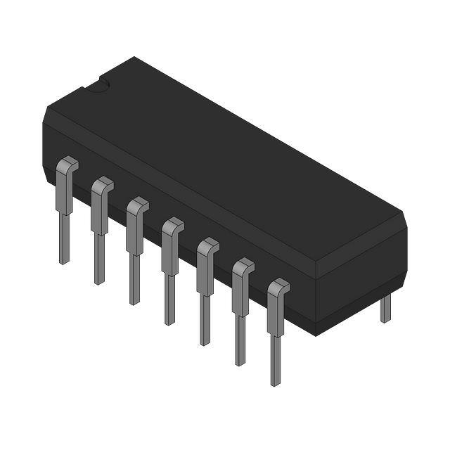
D, N, OR PW PACKAGE
(TOP VIEW)
Low Supply Current . . . 85 µA Typ
Low Offset Voltage . . . 2 mV Typ
Low Input Bias Current . . . 2 nA Typ
Input Common Mode to GND
Wide Supply Voltage . . . 3 V < VCC < 32 V
Pin Compatible With LM324
Applications
– LCD Displays
– Portable Instrumentation
– Sensor/Metering Equipment
– Consumer Electronics (MP3 Players, Toys,
Etc.)
– Power Supplies
1OUT
1IN−
1IN+
VCC
2IN+
2IN−
2OUT
1
14
2
13
3
12
4
11
5
10
6
9
7
8
4OUT
4IN−
4IN+
GND
3IN+
3IN−
3OUT
DESCRIPTION/ORDERING INFORMATION
The LP324 and LP2902 are quadruple low-power operational amplifiers especially suited for battery-operated
applications. Good input specifications and wide supply-voltage range still are achieved, despite the ultra-low
supply current. Single-supply operation is achieved with an input common-mode range that includes GND.
The LP324 and LP2902 are ideal in applications where wide supply voltage and low power are more important
than speed and bandwidth. These applications include portable instrumentation, LCD displays, consumer
electronics (MP3 players, toys, etc.), and power supplies.
ORDERING INFORMATION
PACKAGE (1)
TA
PDIP – N
0°C to 70°C
SOIC – D
TSSOP – PW
PDIP – N
–40°C to 85°C
SOIC – D
TSSOP – PW
(1)
ORDERABLE PART NUMBER
Tube of 25
LP324N
Tube of 50
LP324D
Reel of 2500
LP324DR
Tube of 90
LP324PW
Reel of 2000
LP324PWR
Tube of 25
LP2902N
Tube of 50
LP2902D
Reel of 2500
LP2902DR
Tube of 50
LP2902PW
Reel of 2500
LP2902PWR
TOP-SIDE MARKING
LP324N
LP324
LP324
LP2902N
LP2902
LP2902
Package drawings, standard packing quantities, thermal data, symbolization, and PCB design guidelines are available at
www.ti.com/sc/package.
SYMBOL (EACH AMPLIFIER)
−
IN−
OUT
+
IN+
Please be aware that an important notice concerning availability, standard warranty, and use in critical applications of Texas
Instruments semiconductor products and disclaimers thereto appears at the end of this data sheet.
PRODUCTION DATA information is current as of publication date.
Products conform to specifications per the terms of the Texas
Instruments standard warranty. Production processing does not
necessarily include testing of all parameters.
Copyright © 2005, Texas Instruments Incorporated
�LP324, LP2902
ULTRA-LOW-POWER QUADRUPLE OPERATIONAL AMPLIFIERS
www.ti.com
SLOS460A – MARCH 2005 – REVISED MAY 2005
SCHEMATIC (EACH AMPLIFIER)
VCC
OUT
IN−
IN+
Absolute Maximum Ratings (1)
over operating free-air temperature range (unless otherwise noted)
MIN
VCC
MAX
Supply voltage range (2)
V
±32
V
32
V
voltage (3)
VID
Differential input
VI
Input voltage (either input)
–0.3
Duration of output short circuit (one amplifier) to ground at (or below) TA = 25°C, VCC ≤ 15 V (4)
Unlimited
D package
θJA
Package thermal
impedance (5) (6)
86
N package
80
PW package
TJ
Operating virtual junction temperature
Tstg
Storage temperature range
(1)
(2)
(3)
(4)
(5)
(6)
UNIT
±16 or 32
°C/W
113
–65
150
°C
150
°C
Stresses beyond those listed under "absolute maximum ratings" may cause permanent damage to the device. These are stress ratings
only, and functional operation of the device at these or any other conditions beyond those indicated under "recommended operating
conditions" is not implied. Exposure to absolute-maximum-rated conditions for extended periods may affect device reliability.
All voltage values (except differential voltages and VCC specified for the measurement of IOS) are with respect to the network GND.
Differential voltages are at IN+, with respect to IN–.
Short circuits from outputs to VCC can cause excessive heating and eventual destruction.
Maximum power dissipation is a function of TJ(max), θJA, and TA. The maximum allowable power dissipation at any allowable ambient
temperature is PD = (TJ(max) – TA)/θJA. Operating at the absolute maximum TJ of 150°C can affect reliability.
The package thermal impedance is calculated in accordance with JESD 51-7.
ESD Protection
TEST CONDITIONS
Human-Body Model
2
TYP
UNIT
±2
kV
�LP324, LP2902
ULTRA-LOW-POWER QUADRUPLE OPERATIONAL AMPLIFIERS
www.ti.com
SLOS460A – MARCH 2005 – REVISED MAY 2005
Electrical Characteristics
TA = 25°C, VCC = 5 V, VIC = VCC/2, RL = 100 kΩ to GND (unless otherwise noted)
PARAMETER
TEST CONDITIONS (1)
TA (2)
LP324
MAX
MIN TYP (3)
MAX
2
4
2
4
25°C
VIO
Input offset voltage
IIB
Input bias current
IIO
Input offset current
AV
Large-signal
voltage gain
RL = 10 kΩ to GND,
VCC = 30 V
25°C
50
Full range
40
CMRR
Common-mode
rejection ratio
VCC = 30 V,
VIC = 0 V to VCC – 1.5 V
25°C
80
Full range
75
kVSR
Power-supply
rejection ratio
VCC = 5 V to 30 V
25°C
80
Full range
75
ICC
Supply current
RL = ∞
VOH
Output voltage
swing (high)
IL = 0.35 mA to GND,
VIC = 0 V
VOL
Output voltage
swing (low)
IL = 0.35 mA from VCC,
VIC = 0 V
IO
Output source
current
VO = 3 V, VID = 1 V
Full range
9
25°C
2
Full range
25°C
0.2
25°C
Output sink current
VO = 1.5 V, VID = –1 V,
VIC = 0 V
25°C
25°C
2
2
0.5
40
70
90
80
90
80
90
85
1
25°C
7
Full range
4
25°C
4
Full range
3
25°C
2
Full range
1
150
275
3.6
3.4
3.6
0.82
0.7
7
10
mA
4
5
4
5
3
4
2
µA
V
1
10
nA
V
VCC – 1.9
0.7
nA
V
75
150
mV
dB
75
90
UNIT
V/mV
30
VCC – 1.9
0.82
4
8
250
3.4
20
40
100
85
Full range
25°C
10
4
Full range
Full range
10
20
Full range
VO = 1.5 V, VID = –1 V
IO
LP2902
MIN TYP (3)
mA
4
1
20
35
20
35
IOS,GND
Output short to GND VID = 1 V
IOS,VCC
Output short to VCC
∝VIO
Input offset
voltage drift
25°C
10
10
µV/°C
∝IIO
Input offset
current drift
25°C
10
10
pA/°C
(1)
(2)
(3)
VID = –1 V
Full range
25°C
40
15
Full range
30
40
15
45
30
45
mA
mA
For full-range temperature limits: VCC = 3 V to 32 V, VICR = 0 V to VCC – 1.5 V (unless otherwise noted)
Full range is 0°C to 70°C for LP324 and –40°C to 85°C for LP2902.
All typical values are at TA = 25°C.
Operating Conditions
VCC = ±15 V, TA = 25°C
PARAMETER
TYP
UNIT
GBW
Gain bandwidth product
100
kHz
SR
Slew rate
50
V/ms
3
�PACKAGE OPTION ADDENDUM
www.ti.com
14-Oct-2022
PACKAGING INFORMATION
Orderable Device
Status
(1)
Package Type Package Pins Package
Drawing
Qty
Eco Plan
(2)
Lead finish/
Ball material
MSL Peak Temp
Op Temp (°C)
Device Marking
(3)
Samples
(4/5)
(6)
LP2902D
ACTIVE
SOIC
D
14
50
RoHS & Green
NIPDAU
Level-1-260C-UNLIM
-40 to 85
LP2902
Samples
LP2902DR
ACTIVE
SOIC
D
14
2500
RoHS & Green
NIPDAU
Level-1-260C-UNLIM
-40 to 85
LP2902
Samples
LP2902N
ACTIVE
PDIP
N
14
25
RoHS & Green
NIPDAU
N / A for Pkg Type
-40 to 85
LP2902N
Samples
LP2902PW
ACTIVE
TSSOP
PW
14
90
RoHS & Green
NIPDAU
Level-1-260C-UNLIM
-40 to 85
LP2902
Samples
LP2902PWR
ACTIVE
TSSOP
PW
14
2000
RoHS & Green
NIPDAU
Level-1-260C-UNLIM
-40 to 85
LP2902
Samples
LP2902PWRE4
ACTIVE
TSSOP
PW
14
2000
RoHS & Green
NIPDAU
Level-1-260C-UNLIM
-40 to 85
LP2902
Samples
LP324D
ACTIVE
SOIC
D
14
50
RoHS & Green
NIPDAU
Level-1-260C-UNLIM
0 to 70
LP324
Samples
LP324DR
ACTIVE
SOIC
D
14
2500
RoHS & Green
NIPDAU | SN
Level-1-260C-UNLIM
0 to 70
LP324
Samples
LP324DRG4
ACTIVE
SOIC
D
14
2500
RoHS & Green
NIPDAU
Level-1-260C-UNLIM
0 to 70
LP324
Samples
LP324N
ACTIVE
PDIP
N
14
25
RoHS & Green
NIPDAU
N / A for Pkg Type
0 to 70
LP324N
Samples
LP324PW
ACTIVE
TSSOP
PW
14
90
RoHS & Green
NIPDAU
Level-1-260C-UNLIM
0 to 70
LP324
Samples
LP324PWR
ACTIVE
TSSOP
PW
14
2000
RoHS & Green
NIPDAU
Level-1-260C-UNLIM
0 to 70
LP324
Samples
(1)
The marketing status values are defined as follows:
ACTIVE: Product device recommended for new designs.
LIFEBUY: TI has announced that the device will be discontinued, and a lifetime-buy period is in effect.
NRND: Not recommended for new designs. Device is in production to support existing customers, but TI does not recommend using this part in a new design.
PREVIEW: Device has been announced but is not in production. Samples may or may not be available.
OBSOLETE: TI has discontinued the production of the device.
(2)
RoHS: TI defines "RoHS" to mean semiconductor products that are compliant with the current EU RoHS requirements for all 10 RoHS substances, including the requirement that RoHS substance
do not exceed 0.1% by weight in homogeneous materials. Where designed to be soldered at high temperatures, "RoHS" products are suitable for use in specified lead-free processes. TI may
reference these types of products as "Pb-Free".
RoHS Exempt: TI defines "RoHS Exempt" to mean products that contain lead but are compliant with EU RoHS pursuant to a specific EU RoHS exemption.
Green: TI defines "Green" to mean the content of Chlorine (Cl) and Bromine (Br) based flame retardants meet JS709B low halogen requirements of
很抱歉,暂时无法提供与“LP2902N”相匹配的价格&库存,您可以联系我们找货
免费人工找货