User's Guide
SNVA265A – November 2007 – Revised April 2013
AN-1675 LP38511TS-1.8 Evaluation Board
1
Introduction
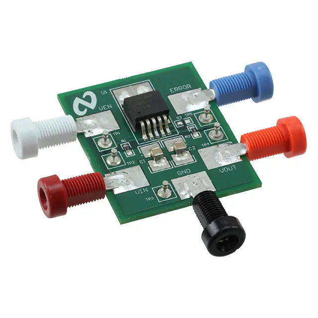
This board is designed to enable the evaluation of the LP38511TS-1.8 Voltage Regulator. Each board is
assembled and tested in the factory. This evaluation board has the TO-263 5–lead package mounted.
2
General Description
The LP38511 is a linear regulator capable of supplying up to 800 mA of output current, and incorporates
Enable and Error flag features.
The device has been designed to work with 10 µF ceramic input and output capacitors. Footprints areas
for CIN and COUT will allow for a variety of sizes.
3
Operation
The input voltage, applied between VIN and GND, should be at least 2.25V, and no higher than 5.5V.
Loads can be connected to VOUT with reference to GND.
Test points are provided on the board to allow monitoring of VOUT, VIN, Enable, and ERROR signals during
operation
If the application does not require the Enable function, the EN pin should be connected to directly to the
adjacent VIN pin.
4
Enable Operation
The Enable On threshold is typically 1.2V, and typically has 200mV of hysteresis. The voltage signal
should rise and fall cleanly, and promptly, through these thresholds.
The Enable pin (EN) has no internal pull-up or pull-down to establish a default condition and, as a result,
this pin must be terminated either actively or passively.
Figure 1. VOUT vs. VEN
All trademarks are the property of their respective owners.
SNVA265A – November 2007 – Revised April 2013
Submit Documentation Feedback
AN-1675 LP38511TS-1.8 Evaluation Board
Copyright © 2007–2013, Texas Instruments Incorporated
1
�ERROR Flag
www.ti.com
If the Enable pin is driven from a single ended device (such as the collector of a discrete transistor) a pullup resistor to VIN, or a pull-down resistor to ground, will be required for proper operation. A 1 kΩ to 100 kΩ
resistor can be used as the pull-up or pull-down resistor to establish default condition for the EN pin. The
resistor value selected should be appropriate to swamp out any leakage in the external single ended
device, as well as any stray capacitance.
If the Enable pin is driven from a source that actively pulls high and low (such as a CMOS rail to rail
comparator output), the pull-up, or pull-down, resistor is not required.
If the application does not require the Enable function, the EN pin should be connected to directly to the
adjacent VIN pin.
The status of the Enable pin also affects the behavior of the ERROR Flag. While the Enable pin is high
the regulator control loop will be active and the ERROR Flag will report the status of the output voltage.
When the Enable pin is taken low the regulator control loop is shutdown, the output is turned off, and the
internal logic will immediately force the ERROR Flag pin low.
Figure 2. Enable Threshold
5
ERROR Flag
When the LP38511 Enable pin is high, the ERROR Flag pin will produce a logic low signal when the
output drops by more than 10% (typical) from the nominal output voltage. The drop in output voltage may
be due to low input voltage, current limiting, or thermal limiting. This flag has a built in hysteresis. The
output voltage will need to rise to within 5% of the nominal output voltage for the ERROR Flag to return to
a logic high state. It should also be noted that when the Enable pin is pulled low, the ERROR Flag pin is
forced to be low as well.
The internal ERROR flag comparator has an open drain output stage. Hence, the ERROR pin requires an
external pull-up resistor. The value of the pull-up resistor should be in the range of 2 kΩ to 100 kΩ, and
should be connected to the LP38511 output voltage pin. The ERROR Flag pin should not be pulled-up to
any voltage source higher than VIN as current flow through an internal parasitic diode may cause
unexpected behavior. When the input voltage is less than typically 1.25V the status of the ERROR flag
output will not be reliable. The ERROR Flag pin must be connected to ground if this function is not used.
The timing diagram in Figure 4 shows the relationship between the ERROR flag and the output voltage
when the pull-up resistor is connected to the output voltage pin.
The timing diagram in Figure 5 shows the relationship between the ERROR flag and the output voltage
when the pull-up resistor is connected to the input voltage pin.
6
Power Dissipation
The TO-263 package alone has a junction to ambient thermal resistance (θJA) rating of 60°C/W. When
mounted on the LP38511TS evaluation board the θJA rating is approximately 30°C/W.
2
AN-1675 LP38511TS-1.8 Evaluation Board
SNVA265A – November 2007 – Revised April 2013
Submit Documentation Feedback
Copyright © 2007–2013, Texas Instruments Incorporated
�Power Dissipation
www.ti.com
Although there is only approximately 0.28 square inches of copper area immediately under the tab, the top
copper surface area is extended to additional copper area on the bottom of the board by nine thermal
vias.
With the 30°C/W thermal rating the LP38511TS evaluation board will deliver the rated 3A output current if
VIN = 2.5V, VOUT = 1.8V, and TA ≤ 25°C.
Figure 3. Maximum Power Dissipation vs. Ambient Temperature
~2.50V
~2.25V
VIN
~1.55V
~1.25V
Load
Transient
Power-Up
NOM
~90%
~85%
Line
Transient
Power-Down
VOUT
1.80V
VERROR
Figure 4. ERROR Flag when Pull-Up is from VOUT
SNVA265A – November 2007 – Revised April 2013
Submit Documentation Feedback
AN-1675 LP38511TS-1.8 Evaluation Board
Copyright © 2007–2013, Texas Instruments Incorporated
3
�Connection Diagram
www.ti.com
~2.50V
~2.25V
VIN
~1.55V
~1.25V
Load
Transient
Power-Up
NOM
~90%
~85%
Line
Transient
Power-Down
VOUT
~2.50V
VERROR
~1.25V
Figure 5. ERROR Flag when Pull-Up is from VIN
7
Connection Diagram
IN 2
GND 3
OUT 4
ERROR 5
8
TAB
IS
GND
LP38511TS-1.8
EN 1
Schematic Diagram
TP1
VIN
VERROR
TP5 TP3 TP4
VERR GND VOUT
TP2
VEN
J5
R2
10 k:
VIN
J2
IN (2)
C1
10 PF
Ceramic
R1
10 k:
VEN
GND
VOUT
C2
10 PF
Ceramic
LP38511TS-1.8
EN (1)
J1
J4
(4) OUT
(5) ERROR
GND (3)
J3
Figure 6. Evaluation Board Schematic
4
AN-1675 LP38511TS-1.8 Evaluation Board
SNVA265A – November 2007 – Revised April 2013
Submit Documentation Feedback
Copyright © 2007–2013, Texas Instruments Incorporated
�PCB Layout
www.ti.com
9
PCB Layout
Figure 7. Evaluation Board Component and Pin Layout
10
Bill of Materials
ID
Name
Description
Manufacturer
Part Number
U1
U1
LP38511
Texas Instruments
LP38511TS-1.8 NOPB
C1
CIN
10 µF, 10%, MLCC, 10V, X7R, 1210
AVX
1210ZC106KAT2A
C2
COUT
10 µF, 10%, MLCC, 10V, X7R, 1210
AXV
1210ZC106KAT2A
J1
VEN
Banana Jack : Insulated Solder
Terminal ; White
108–0901–001
J2
VIN
Banana Jack : Insulated Solder
Terminal ; Red
108–0902–001
J3
GND
Banana Jack : Insulated Solder
Terminal ; Black
J4
VOUT
Banana Jack : Insulated Solder
Terminal ; Orange
108–0906–001
J5
VERR
Banana Jack : Insulated Solder
Terminal ; Blue
108–0910–001
R1
—
Resistor: 10 kΩ ±1%; 0805
Vishay Dale
CRCW 0805 1002 F
R2
—
Resistor: 10 kΩ ±1%; 0805
Vishay Dale
CRCW 0805 1002 F
R3
—
Not Installed
N/A
N/A
TP1
TPEN
Turret Terminal :
Mounting Hole Diameter = 0.062”
Keystone
1593-2
TP2
TPIN
TP3
TPGND
TP4
TPOUT
TP5
TPBIAS
SNVA265A – November 2007 – Revised April 2013
Submit Documentation Feedback
Johnson Components
108–0903–001
AN-1675 LP38511TS-1.8 Evaluation Board
Copyright © 2007–2013, Texas Instruments Incorporated
5
�Bill of Materials
6
www.ti.com
AN-1675 LP38511TS-1.8 Evaluation Board
SNVA265A – November 2007 – Revised April 2013
Submit Documentation Feedback
Copyright © 2007–2013, Texas Instruments Incorporated
�IMPORTANT NOTICE
Texas Instruments Incorporated and its subsidiaries (TI) reserve the right to make corrections, enhancements, improvements and other
changes to its semiconductor products and services per JESD46, latest issue, and to discontinue any product or service per JESD48, latest
issue. Buyers should obtain the latest relevant information before placing orders and should verify that such information is current and
complete. All semiconductor products (also referred to herein as “components”) are sold subject to TI’s terms and conditions of sale
supplied at the time of order acknowledgment.
TI warrants performance of its components to the specifications applicable at the time of sale, in accordance with the warranty in TI’s terms
and conditions of sale of semiconductor products. Testing and other quality control techniques are used to the extent TI deems necessary
to support this warranty. Except where mandated by applicable law, testing of all parameters of each component is not necessarily
performed.
TI assumes no liability for applications assistance or the design of Buyers’ products. Buyers are responsible for their products and
applications using TI components. To minimize the risks associated with Buyers’ products and applications, Buyers should provide
adequate design and operating safeguards.
TI does not warrant or represent that any license, either express or implied, is granted under any patent right, copyright, mask work right, or
other intellectual property right relating to any combination, machine, or process in which TI components or services are used. Information
published by TI regarding third-party products or services does not constitute a license to use such products or services or a warranty or
endorsement thereof. Use of such information may require a license from a third party under the patents or other intellectual property of the
third party, or a license from TI under the patents or other intellectual property of TI.
Reproduction of significant portions of TI information in TI data books or data sheets is permissible only if reproduction is without alteration
and is accompanied by all associated warranties, conditions, limitations, and notices. TI is not responsible or liable for such altered
documentation. Information of third parties may be subject to additional restrictions.
Resale of TI components or services with statements different from or beyond the parameters stated by TI for that component or service
voids all express and any implied warranties for the associated TI component or service and is an unfair and deceptive business practice.
TI is not responsible or liable for any such statements.
Buyer acknowledges and agrees that it is solely responsible for compliance with all legal, regulatory and safety-related requirements
concerning its products, and any use of TI components in its applications, notwithstanding any applications-related information or support
that may be provided by TI. Buyer represents and agrees that it has all the necessary expertise to create and implement safeguards which
anticipate dangerous consequences of failures, monitor failures and their consequences, lessen the likelihood of failures that might cause
harm and take appropriate remedial actions. Buyer will fully indemnify TI and its representatives against any damages arising out of the use
of any TI components in safety-critical applications.
In some cases, TI components may be promoted specifically to facilitate safety-related applications. With such components, TI’s goal is to
help enable customers to design and create their own end-product solutions that meet applicable functional safety standards and
requirements. Nonetheless, such components are subject to these terms.
No TI components are authorized for use in FDA Class III (or similar life-critical medical equipment) unless authorized officers of the parties
have executed a special agreement specifically governing such use.
Only those TI components which TI has specifically designated as military grade or “enhanced plastic” are designed and intended for use in
military/aerospace applications or environments. Buyer acknowledges and agrees that any military or aerospace use of TI components
which have not been so designated is solely at the Buyer's risk, and that Buyer is solely responsible for compliance with all legal and
regulatory requirements in connection with such use.
TI has specifically designated certain components as meeting ISO/TS16949 requirements, mainly for automotive use. In any case of use of
non-designated products, TI will not be responsible for any failure to meet ISO/TS16949.
Products
Applications
Audio
www.ti.com/audio
Automotive and Transportation
www.ti.com/automotive
Amplifiers
amplifier.ti.com
Communications and Telecom
www.ti.com/communications
Data Converters
dataconverter.ti.com
Computers and Peripherals
www.ti.com/computers
DLP® Products
www.dlp.com
Consumer Electronics
www.ti.com/consumer-apps
DSP
dsp.ti.com
Energy and Lighting
www.ti.com/energy
Clocks and Timers
www.ti.com/clocks
Industrial
www.ti.com/industrial
Interface
interface.ti.com
Medical
www.ti.com/medical
Logic
logic.ti.com
Security
www.ti.com/security
Power Mgmt
power.ti.com
Space, Avionics and Defense
www.ti.com/space-avionics-defense
Microcontrollers
microcontroller.ti.com
Video and Imaging
www.ti.com/video
RFID
www.ti-rfid.com
OMAP Applications Processors
www.ti.com/omap
TI E2E Community
e2e.ti.com
Wireless Connectivity
www.ti.com/wirelessconnectivity
Mailing Address: Texas Instruments, Post Office Box 655303, Dallas, Texas 75265
Copyright © 2013, Texas Instruments Incorporated
�