LP38512MR-ADJEV/NOPB 数据手册
User's Guide
SNVA351B – March 2009 – Revised April 2013
AN-1859 LP38512MR-ADJ Evaluation Board
1
Introduction
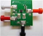
This board is designed to allow the evaluation of the LP38512MR-ADJ Voltage Regulator. Each board is
assembled and tested in the factory. This evaluation board has the PSOP-8 package mounted, and the
output voltage is set to 1.20V.
2
General Description
The LP38512MR-ADJ is an adjustable LDO linear regulator capable of supplying up to 1.5A of output
current, and incorporates an Enable function.
The device has been designed to work with 10 µF input and output ceramic capacitors. Footprints areas
for CIN and COUT will allow for a variety of sizes.
3
Operation
The input voltage, applied between VIN and GND, should be at least 2.25V, or at least 500 mV greater
than VOUT, whichever value is larger. The input voltage should be no greater than 5.5V, which is the high
end of the Operating Rating voltage.
Loads can be connected to VOUT with reference to GND.
VOUT and VIN test points are provided on the board to allow accurate measurements directly onto the input
and output pins of the device, eliminating any voltage drop on the PCB traces or connecting wires to the
load.
4
Setting VOUT
The output voltage is set using the external resistive divider R1 and R2. The output voltage is given by the
formula:
VOUT = VADJ × (1 + (R1 / R2))
(1)
It is recommended that the values selected for R1 and R2 are such that the parallel value is less than
1.00 kΩ. This is to prevent internal parasitic capacitances on the ADJ pin from interfering with the FZ pole
set by R1 and CFF.
( (R1 × R2) / (R1 + R2) ) ≤ 1.00 kΩ
(2)
Table 1 lists some suggested, best fit, standard ±1% resistor values for R1 and R2, and a standard ±10%
capacitor values for CFF, for a range of VOUT values. Other values of R1, R2, and CFF are available that will
give similar results.
Refer to AN-1378 Method for Calculating Output Voltage Tolerances in Adjustable Regulators Application
Report (SNVA112) for additional information on how resistor tolerances affect the calculated VOUT value.
The LP38512MR-ADJ Evaluation board is assembled with a 1.40 kΩ ±1% resistor for R1, and a
1.00 kΩ ±1% resistor for R2. This sets VOUT to 1.20V.
VOUT = 500 mV × (1 + (1.40 kΩ / 1.00 kΩ ) )
(3)
All trademarks are the property of their respective owners.
SNVA351B – March 2009 – Revised April 2013
Submit Documentation Feedback
AN-1859 LP38512MR-ADJ Evaluation Board
Copyright © 2009–2013, Texas Instruments Incorporated
1
�Selecting CFF
www.ti.com
Table 1. Suggested Components
5
VOUT
R1
R2
CFF
FZ
0.80V
1.07 kΩ
1.78 kΩ
4700 pF
31.6 kHz
1.00V
1.00 kΩ
1.00 kΩ
4700 pF
33.8 kHz
1.20V
1.40 kΩ
1.00 kΩ
3300 pF
34.4 kHz
1.50V
2.00 kΩ
1.00 kΩ
2700 pF
29.5 kHz
1.80V
2.94 kΩ
1.13 kΩ
1500 pF
36.1 kHz
2.00V
1.02 kΩ
340Ω
4700 pF
33.2 kHz
2.50V
1.02 kΩ
255Ω
4700 pF
33.2 kHz
3.00V
1.00 kΩ
200Ω
4700 pF
33.8 kHz
3.30V
2.00 kΩ
357Ω
2700 pF
29.5 kHz
Selecting CFF
A capacitor placed across the gain resistor R1 will provide additional phase margin to improve load
transient response of the device. This capacitor, CFF, in parallel with R1, will form a zero in the loop
response given by the formula:
FZ = (1 / (2 × π × CFF × R1) )
(4)
The value for CFF should be selected to set a zero frequency (FZ) between 25 kHz and 50 kHz using the
formula:
CFF = 1 / (2 × π × FZ × R1)
(5)
The closest standard 10% value is usually adequate for CFF.
The LP38512MR-ADJ Evaluation board is assembled with a 3300 pF capacitor for CFF. This sets FZ to
approximately 34 kHz.
FZ = (1 / (2 × π × 3300 pF × 1.40kΩ ) ) = 34.4 kHz
Figure 1. 10 mA to 1.5A Load Transient Response
2
(6)
Figure 2. 500 mA to 1.5A Load Transient Response
AN-1859 LP38512MR-ADJ Evaluation Board
Copyright © 2009–2013, Texas Instruments Incorporated
SNVA351B – March 2009 – Revised April 2013
Submit Documentation Feedback
�Enable Function
www.ti.com
6
Enable Function
ON/OFF control is provided by supplying a logic level signal to the Enable pin. A minimum VEN value of
1.2V is typically required at this pin to enable the LDO output. The LDO output will be shutdown when the
VEN value is typically 0.6V or less. The VEN threshold incorporates approximately 100 mV of hysteresis.
In applications where the LP38512MR-ADJ is operated continuously the Enable pin can be connected
directly to VIN. The Enable pin has no default bias and must not be left floating. The Enable pin must be
actively driven to the appropriate voltage level.
Figure 3. VOUT vs VEN
7
Figure 4. Enable Thresholds
Power Dissipation
The PSOP-8 package alone has a junction to ambient thermal resistance (θJA) rating of 168°C/W when
mounted to the minimum land area (EIA/JESD51-3). When mounted on the LP38512MR-ADJ Evaluation
Board the θJA rating is approximately 40°C/W.
The exposed DAP is soldered to the copper area immediately under the package. The top copper surface
area is extended to additional copper area on the bottom of the board by five thermal vias placed inside
the DAP land area.
With the 40°C/W thermal rating the LP38512MR-ADJ evaluation board will dissipate a maximum of 2.5W
with TA = 25°C.
Figure 5. Maximum Power Dissipation vs Ambient Temperature
SNVA351B – March 2009 – Revised April 2013
Submit Documentation Feedback
AN-1859 LP38512MR-ADJ Evaluation Board
Copyright © 2009–2013, Texas Instruments Incorporated
3
�Pin Out
8
www.ti.com
Pin Out
OUT 1
8 IN
OUT 2
7 IN
ADJ 3
6 EN
N/C 4
5 GND
DAP
Connect to GND
Figure 6. Pin Out
9
Schematic Diagram
TP1 TP2 TP3
TP4
LP38512MR-ADJ
IN (8)
IN (7)
VIN (J2)
(1) OUT
(2) OUT
1.20V
VOUT (J4)
C1
10 PF
R3
10 k:
R1
1.40 k:
EN (6)
VEN (J1)
GND (5)
(3) ADJ
DAP
C3
3300 pF
C2
10 PF
R2
1.00 k:
GND (J3)
Figure 7. Evaluation Board Schematic.
4
AN-1859 LP38512MR-ADJ Evaluation Board
Copyright © 2009–2013, Texas Instruments Incorporated
SNVA351B – March 2009 – Revised April 2013
Submit Documentation Feedback
�Bill of Materials
www.ti.com
10
Bill of Materials
Table 2. Bill of Materials
ID
Name
Description
Manufacturer
PCB
PCB
Printed Circuit Board
Texas Instruments
600174
U1
U1
LP38512
Texas Instruments
LP38512
C1
CIN
Capacitor: 10 µF; ±10%; MLCC; 10V;
X7R; 1210
C2
COUT
Capacitor: 10 µF;, ±10%; MLCC; 10V;
X7R; 1210
C3
CFF
Capacitor: 3300 pF;, ±10%; MLCC;
50V; X7R; 0805
J1
VEN
Banana Jack : Insulated Solder
Terminal; White
J2
VIN
Banana Jack : Insulated Solder
Terminal; Red
Part Number
1210ZC106KAT2A
AVX
1210ZC106KAT2A
KEMET
C0805C332K5RAC
108-0901-001
108-0902-001
Johnson Components
J3
GND
Banana Jack : Insulated Solder
Terminal; Black
J4
VOUT
Banana Jack : Insulated Solder
Terminal; Orange
108-0906-001
R1
R1
Resistor: 1.40 kΩ, ±1%; Thick Film;
125 mW; ±100 ppm; 0805
CRCW08051K40FK
R2
R2
Resistor: 1.00 kΩ, ±1%; Thick Film;
125 mW; ±100 ppm; 0805
R3
R3
Resistor: 10.0 kΩ, ±1%; Thick Film;
125 mW; ±100 ppm; 0805
TP1
TPEN
TP2
TPIN
TP3
TPGND
TP4
TPOUT
Turret Terminal : Mounting Hole
Diameter = 0.062”
SNVA351B – March 2009 – Revised April 2013
Submit Documentation Feedback
108-0903-001
VISHAY DALE
CRCW08051K00FK
CRCW080510K0FK
Keystone
1593–2
AN-1859 LP38512MR-ADJ Evaluation Board
Copyright © 2009–2013, Texas Instruments Incorporated
5
�PCB Layout
11
www.ti.com
PCB Layout
R2
1.00 k:
R1
1.40 k:
R2
ENABLE
CFF (C3)
VEN
3300 pF
R1
J1
C3
U1
TP1
J4
R3
R3
10 k:
VOUT
VOUT
TP2
TP4
VIN
J2
C1
C2
VIN
GND
TP3
J3
CIN (C1)
10 PF
COUT (C2)
10 PF
GND
Figure 8. Evaluation Board Component and Pin Layout
6
AN-1859 LP38512MR-ADJ Evaluation Board
Copyright © 2009–2013, Texas Instruments Incorporated
SNVA351B – March 2009 – Revised April 2013
Submit Documentation Feedback
�PCB Layout
www.ti.com
Figure 9. Top Side Copper Area
Figure 10. Bottom Side Copper Area
SNVA351B – March 2009 – Revised April 2013
Submit Documentation Feedback
AN-1859 LP38512MR-ADJ Evaluation Board
Copyright © 2009–2013, Texas Instruments Incorporated
7
�IMPORTANT NOTICE
Texas Instruments Incorporated and its subsidiaries (TI) reserve the right to make corrections, enhancements, improvements and other
changes to its semiconductor products and services per JESD46, latest issue, and to discontinue any product or service per JESD48, latest
issue. Buyers should obtain the latest relevant information before placing orders and should verify that such information is current and
complete. All semiconductor products (also referred to herein as “components”) are sold subject to TI’s terms and conditions of sale
supplied at the time of order acknowledgment.
TI warrants performance of its components to the specifications applicable at the time of sale, in accordance with the warranty in TI’s terms
and conditions of sale of semiconductor products. Testing and other quality control techniques are used to the extent TI deems necessary
to support this warranty. Except where mandated by applicable law, testing of all parameters of each component is not necessarily
performed.
TI assumes no liability for applications assistance or the design of Buyers’ products. Buyers are responsible for their products and
applications using TI components. To minimize the risks associated with Buyers’ products and applications, Buyers should provide
adequate design and operating safeguards.
TI does not warrant or represent that any license, either express or implied, is granted under any patent right, copyright, mask work right, or
other intellectual property right relating to any combination, machine, or process in which TI components or services are used. Information
published by TI regarding third-party products or services does not constitute a license to use such products or services or a warranty or
endorsement thereof. Use of such information may require a license from a third party under the patents or other intellectual property of the
third party, or a license from TI under the patents or other intellectual property of TI.
Reproduction of significant portions of TI information in TI data books or data sheets is permissible only if reproduction is without alteration
and is accompanied by all associated warranties, conditions, limitations, and notices. TI is not responsible or liable for such altered
documentation. Information of third parties may be subject to additional restrictions.
Resale of TI components or services with statements different from or beyond the parameters stated by TI for that component or service
voids all express and any implied warranties for the associated TI component or service and is an unfair and deceptive business practice.
TI is not responsible or liable for any such statements.
Buyer acknowledges and agrees that it is solely responsible for compliance with all legal, regulatory and safety-related requirements
concerning its products, and any use of TI components in its applications, notwithstanding any applications-related information or support
that may be provided by TI. Buyer represents and agrees that it has all the necessary expertise to create and implement safeguards which
anticipate dangerous consequences of failures, monitor failures and their consequences, lessen the likelihood of failures that might cause
harm and take appropriate remedial actions. Buyer will fully indemnify TI and its representatives against any damages arising out of the use
of any TI components in safety-critical applications.
In some cases, TI components may be promoted specifically to facilitate safety-related applications. With such components, TI’s goal is to
help enable customers to design and create their own end-product solutions that meet applicable functional safety standards and
requirements. Nonetheless, such components are subject to these terms.
No TI components are authorized for use in FDA Class III (or similar life-critical medical equipment) unless authorized officers of the parties
have executed a special agreement specifically governing such use.
Only those TI components which TI has specifically designated as military grade or “enhanced plastic” are designed and intended for use in
military/aerospace applications or environments. Buyer acknowledges and agrees that any military or aerospace use of TI components
which have not been so designated is solely at the Buyer's risk, and that Buyer is solely responsible for compliance with all legal and
regulatory requirements in connection with such use.
TI has specifically designated certain components as meeting ISO/TS16949 requirements, mainly for automotive use. In any case of use of
non-designated products, TI will not be responsible for any failure to meet ISO/TS16949.
Products
Applications
Audio
www.ti.com/audio
Automotive and Transportation
www.ti.com/automotive
Amplifiers
amplifier.ti.com
Communications and Telecom
www.ti.com/communications
Data Converters
dataconverter.ti.com
Computers and Peripherals
www.ti.com/computers
DLP® Products
www.dlp.com
Consumer Electronics
www.ti.com/consumer-apps
DSP
dsp.ti.com
Energy and Lighting
www.ti.com/energy
Clocks and Timers
www.ti.com/clocks
Industrial
www.ti.com/industrial
Interface
interface.ti.com
Medical
www.ti.com/medical
Logic
logic.ti.com
Security
www.ti.com/security
Power Mgmt
power.ti.com
Space, Avionics and Defense
www.ti.com/space-avionics-defense
Microcontrollers
microcontroller.ti.com
Video and Imaging
www.ti.com/video
RFID
www.ti-rfid.com
OMAP Applications Processors
www.ti.com/omap
TI E2E Community
e2e.ti.com
Wireless Connectivity
www.ti.com/wirelessconnectivity
Mailing Address: Texas Instruments, Post Office Box 655303, Dallas, Texas 75265
Copyright © 2013, Texas Instruments Incorporated
�