Sample &
Buy
Product
Folder
Support &
Community
Tools &
Software
Technical
Documents
LP38691, LP38693, LP38691-Q1, LP38693-Q1
ZHCSAS0L – JANUARY 2005 – REVISED DECEMBER 2014
LP3869x/-Q1 500mA 低压降 CMOS 线性稳压器
使用陶瓷输出电容器时可保持稳定
1 特性
•
•
1
•
•
•
•
•
•
•
•
•
3 说明
宽输入电压范围(2.7V 至 10V)
所有超薄小外形尺寸无引线封装 (WSON) 选项作为
AEC-Q100 1 级可用
2.0% 输出精度 (25°C)
低压降:500mA(5V 输出典型值)时为 250mV
精密(已调整)带隙基准
可保证 –40°C 至 +125°C 温度范围内的技术规格
1µA 关闭状态静态电流
热过载保护
折返电流限制
TO-252、SOT-223 和 6 凸点晶圆级小外形无引线
(WSON) 封装
使能引脚 (LP38693)
2 应用范围
•
•
•
•
LP3869x 低压降 CMOS 线性稳压器具有严密的输出容
差(典型值 2%)和极低压降(在负载电流为 500A、V
输出= 5V 时为 250mV),并且采用超低等效串联电阻
(ESR) 陶瓷输出电容器,可提供出色的交流性能。
此稳压器采用低热阻的 WSON、SOT-223 以及 TO252 封装,即使在周围温度较高的环境下也可实现满电
流运行。
PMOS 功率晶体管的使用意味着无需直流基极驱动电
流对其进行偏置,因此无论负载电流、输入电压或者运
行温度为何,接地引脚电流均可保持在 100µA 以下。
压降:500mA(5V 输出电压典型值)条件下为
250mV(典型值)
接地引脚电流:满负载时为 55µA(典型值)
硬盘驱动器
笔记本电脑
电池供电设备
便携式仪表
精密输出电压:精度为 2% (25°C)
器件信息(1)
器件型号
LP38691
LP38693
LP38691-Q1
LP38693-Q1
封装
封装尺寸(标称值)
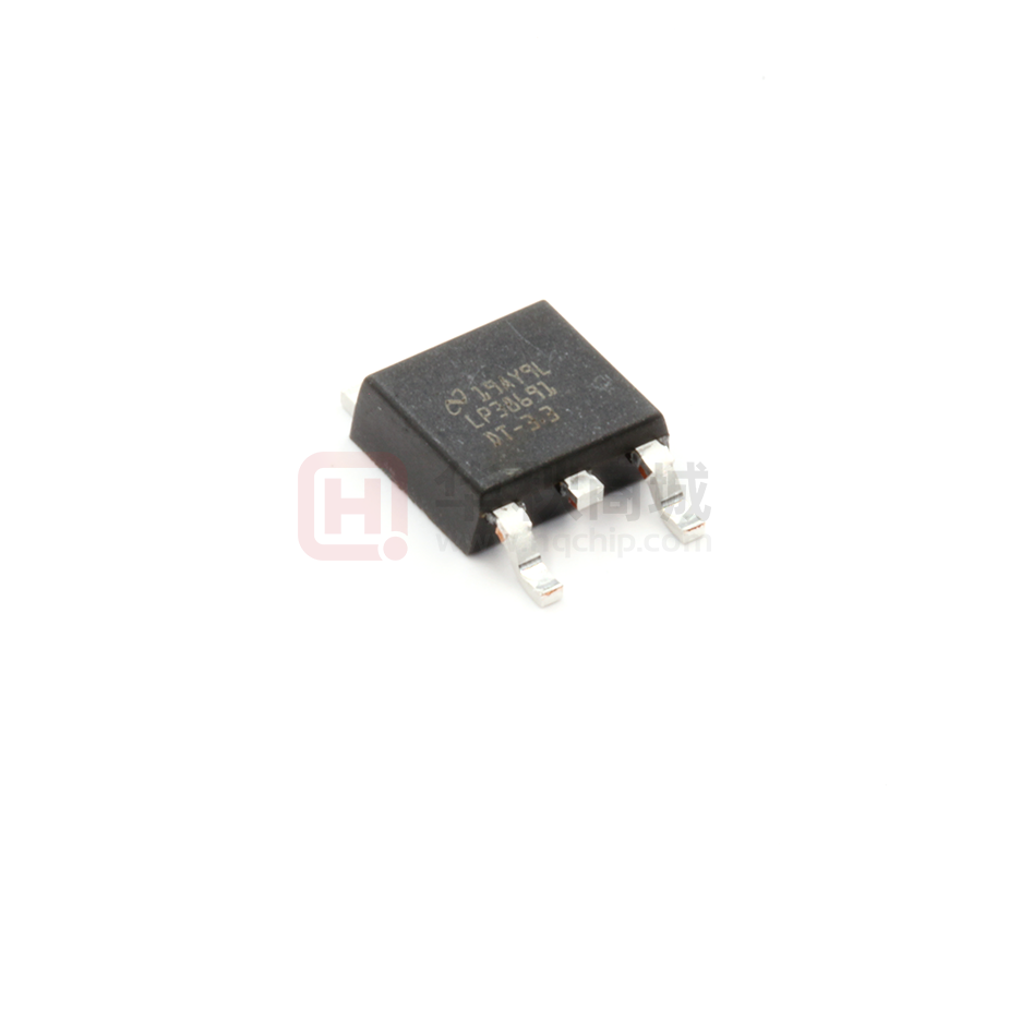
TO-252 (3)
6.58mm x 6.10mm
WSON (6)
3.00mm × 3.00mm
SOT-223 (5)
6.50mm x 3.56mm
WSON (6)
3.00mm × 3.00mm
WSON (6)
3.00mm × 3.00mm
(1) 如需了解所有可用封装,请见数据表末尾的可订购产品附录。
4 典型应用电路
VIN
VOUT
VIN
VIN
VOUT
LP38691
**
SNS
1 PF *
GND
VOUT
VIN
1 PF *
VEN
1 PF *
VEN
VOUT
LP38693
**
SNS
GND
1 PF *
* 稳定状态下的最小值
** 仅限 WSON 封装器件
1
PRODUCTION DATA information is current as of publication date. Products conform to specifications per the terms of the Texas
Instruments standard warranty. Production processing does not necessarily include testing of all parameters.
English Data Sheet: SNVS321
�LP38691, LP38693, LP38691-Q1, LP38693-Q1
ZHCSAS0L – JANUARY 2005 – REVISED DECEMBER 2014
www.ti.com.cn
目录
1
2
3
4
5
6
7
8
特性 ..........................................................................
应用范围...................................................................
说明 ..........................................................................
典型应用电路 ...........................................................
修订历史记录 ...........................................................
Pin Configuration and Functions .........................
Specifications.........................................................
1
1
1
1
2
3
4
7.1
7.2
7.3
7.4
7.5
7.6
7.7
4
4
4
5
5
5
7
Absolute Maximum Ratings ......................................
Handling Ratings: LP3869x ......................................
Handling Ratings: LP3869x-Q1 ................................
Recommended Operating Conditions.......................
Thermal Information ..................................................
Electrical Characteristics...........................................
Typical Characteristics ..............................................
Detailed Description ............................................ 11
8.1 Overview ................................................................. 11
8.2 Functional Block Diagrams ..................................... 11
8.3 Feature Description................................................. 13
8.4 Device Functional Modes........................................ 13
9
Application and Implementation ........................ 14
9.1 Application Information............................................ 14
9.2 Typical Application ................................................. 14
10 Power Supply Recommendations ..................... 19
11 Layout................................................................... 19
11.1 Layout Guidelines ................................................. 19
11.2 Layout Example .................................................... 20
12 器件和文档支持 ..................................................... 21
12.1
12.2
12.3
12.4
相关链接................................................................
商标 .......................................................................
静电放电警告.........................................................
术语表 ...................................................................
21
21
21
21
13 机械封装和可订购信息 .......................................... 21
5 修订历史记录
NOTE: Page numbers for previous revisions may differ from page numbers in the current version.
Changes from Revision K (April 2013) to Revision L
•
Page
已添加 处理额定值表,特性描述部分,器件功能模式,应用和实施部分,电源相关建议部分,布局部分,器件和文档
支持部分以及机械、封装和可订购信息部分 ........................................................................................................................... 1
Changes from Revision J (April 2013) to Revision K
Page
•
Changed layout of National Data Sheet to TI format ........................................................................................................... 18
2
Copyright © 2005–2014, Texas Instruments Incorporated
�LP38691, LP38693, LP38691-Q1, LP38693-Q1
www.ti.com.cn
ZHCSAS0L – JANUARY 2005 – REVISED DECEMBER 2014
6 Pin Configuration and Functions
NDP Package
3-Pin TO-252
Top View
NDC Package
5-Pin SOT-223
Top View
EN 1
N/C 2
5 GND
OUT 3
IN 4
NC - No internal connection
NGG Package
6-Pin WSON With Exposed Thermal Pad
LP38691SD Top View
IN
1
GND
2
N/C
3
Exposed Pad
on Bottom
(DAP)
6
IN
5
SNS
4
OUT
NC - No internal connection
NGG Package
6-Pin WSON With Exposed Thermal Pad
LP38693SD Top View
Copyright © 2005–2014, Texas Instruments Incorporated
IN
1
GND
2
EN
3
Exposed Pad
on Bottom
(DAP)
6
IN
5
SNS
4
OUT
3
�LP38691, LP38693, LP38691-Q1, LP38693-Q1
ZHCSAS0L – JANUARY 2005 – REVISED DECEMBER 2014
www.ti.com.cn
Pin Functions
PIN
NAME
TO252
WSON
SOT223
I/O
DESCRIPTION
3
1, 6
1, 6
4
I
This is the input supply voltage to the regulator. For WSON devices, both VIN
pins must be tied together for full current operation (250mA maximum per pin).
GND
TAB
2
2
5
—
Circuit ground for the regulator. For the PFM and SOT-223 packages this is
thermally connected to the die and functions as a heat sink when the soldered
down to a large copper plane.
SNS
—
5
5
—
I
WSON Only - Output sense pin allows remote sensing at the load which will
eliminate the error in output voltage due to voltage drops caused by the
resistance in the traces between the regulator and the load. This pin must be
tied to VOUT.
EN
—
—
3
1
I
The enable pin allows the part to be turned ON and OFF by pulling this pin high
or low.
OUT
1
4
4
3
O
Regulated output voltage
DAP
—
√
√
—
—
WSON Only - The DAP (Exposed Pad) functions as a thermal connection when
soldered to a copper plane. See WSON Mounting section for more information.
IN
7 Specifications
7.1 Absolute Maximum Ratings (1) (2)
MIN
MAX
UNIT
260
°C
Internally Limited
V
Lead Temp. (Soldering, 5 seconds)
Power Dissipation (3)
V(max) All pins (with respect to GND)
IOUT
–0.3
(4)
Junction Temperature
(1)
(2)
(3)
(4)
12
V
Internally Limited
V
–40
°C
150
Absolute maximum ratings indicate limits beyond which damage to the component may occur. Operating ratings indicate conditions for
which the device is intended to be functional, but do not ensure specific performance limits. For ensured specifications, see Electrical
Characteristics. Specifications do not apply when operating the device outside of its rated operating conditions.
If Military/Aerospace specified devices are required, please contact the Texas Instruments Sales Office/ Distributors for availability and
specifications.
At elevated temperatures, device power dissipation must be derated based on package thermal resistance and heatsink values (if a
heatsink is used). When using the WSON package, refer to AN-1187 Leadless Leadframe Package (LLP), SNOA401, and the WSON
Mounting section in this datasheet. If power dissipation causes the junction temperature to exceed specified limits, the device will go into
thermal shutdown.
If used in a dual-supply system where the regulator load is returned to a negative supply, the output pin must be diode clamped to
ground.
7.2 Handling Ratings: LP3869x
Tstg
Storage temperature range
V(ESD)
(1)
Electrostatic discharge
Human body model (HBM), per ANSI/ESDA/JEDEC JS-001, all
pins (1)
MIN
MAX
UNIT
−65
150
°C
–2
2
kV
JEDEC document JEP155 states that 500-V HBM allows safe manufacturing with a standard ESD control process.
7.3 Handling Ratings: LP3869x-Q1
Tstg
Storage temperature range
V(ESD)
(1)
4
Electrostatic discharge
Human body model (HBM), per ANSI/ESDA/JEDEC JS-001, all
pins (1)
MIN
MAX
UNIT
−65
150
°C
–2
2
kV
JEDEC document JEP155 states that 500-V HBM allows safe manufacturing with a standard ESD control process.
Copyright © 2005–2014, Texas Instruments Incorporated
�LP38691, LP38693, LP38691-Q1, LP38693-Q1
www.ti.com.cn
ZHCSAS0L – JANUARY 2005 – REVISED DECEMBER 2014
7.4 Recommended Operating Conditions
MIN
VIN Supply Voltage
Operating Junction Temperature Range
NOM
MAX
UNIT
2.7
10
V
−40
125
°C
7.5 Thermal Information
THERMAL METRIC (1)
LP38691
LP38693
LP3869x
TO-252
WSON
SOT-223
3 PINS
6 PINS
5 PINS
RθJA (2)
Junction-to-ambient thermal resistance
50.5
50.6
68.5
RθJC(top)
Junction-to-case (top) thermal resistance
52.6
44.4
52.2
RθJB
Junction-to-board thermal resistance
29.7
24.9
13.0
ψJT
Junction-to-top characterization parameter
4.8
0.4
5.5
ψJB
Junction-to-board characterization parameter
29.3
25.1
12.8
RθJC(bot)
Junction-to-case (bottom) thermal resistance
1.5
5.4
n/a
(1)
(2)
UNIT
°C/W
For more information about traditional and new thermal metrics, see the IC Package Thermal Metrics application report, SPRA953.
Junction-to-ambient thermal resistance, High-K.
7.6 Electrical Characteristics
Limits in standard typeface are for TJ = 25°C. Unless otherwise specified: VIN = VOUT + 1 V, CIN = COUT = 10 µF, ILOAD = 10
mA. Min/Max limits are specified through testing, statistical correlation, or design.
PARAMETER
TEST CONDITIONS
VO
Output Voltage Tolerance
100 µA < IL < 0.5 A
VO + 1 V ≤ VIN ≤ 10 V
Full operating temperature range
ΔVO/ΔVIN
Output Voltage Line
Regulation (2)
VO + 0.5 V ≤ VIN ≤ 10 V
IL = 25 mA
MIN
TYP (1)
–2.0
2.0
–4.0
4.0
Output Voltage Load
Regulation (3)
1 mA < IL < 0.5 A
VIN = VO + 1 V
(VO = 2.5 V)
Full operating temperature
range
(VO = 3.3 V)
VIN - VOUT
Dropout Voltage (4)
(VO = 3.3 V)
Full operating temperature
range
(VO = 5 V)
(VO = 5 V)
Full operating temperature
range
(1)
(2)
(3)
(4)
%VOUT
%/V
0.1
1.8
%/A
1 mA < IL < 0.5 A
VIN = VO + 1 V
Full operating temperature range
(VO = 2.5 V)
UNIT
0.03
VO + 0.5 V ≤ VIN ≤ 10 V
IL = 25 mA
Full operating temperature range
ΔVO/ΔIL
MAX
5
IL = 0.1 A
80
IL = 0.5 A
430
IL = 0.1 A
145
IL = 0.5 A
725
IL = 0.1 A
65
IL = 0.5 A
330
IL = 0.1 A
110
IL = 0.5 A
550
IL = 0.1 A
45
IL = 0.5 A
250
IL = 0.1 A
100
IL = 0.5 A
450
mV
Typical numbers represent the most likely parametric norm for 25°C operation.
Output voltage line regulation is defined as the change in output voltage from nominal value resulting from a change in input voltage.
Output voltage load regulation is defined as the change in output voltage from nominal value as the load current increases from 1 mA to
full load.
Dropout voltage is defined as the minimum input to output differential required to maintain the output within 100 mV of nominal value.
Copyright © 2005–2014, Texas Instruments Incorporated
5
�LP38691, LP38693, LP38691-Q1, LP38693-Q1
ZHCSAS0L – JANUARY 2005 – REVISED DECEMBER 2014
www.ti.com.cn
Electrical Characteristics (continued)
Limits in standard typeface are for TJ = 25°C. Unless otherwise specified: VIN = VOUT + 1 V, CIN = COUT = 10 µF, ILOAD = 10
mA. Min/Max limits are specified through testing, statistical correlation, or design.
PARAMETER
IQ
Quiescent Current
TEST CONDITIONS
MIN
VIN ≤ 10 V, IL =100 µA - 0.5 A
TYP (1)
VIN ≤ 10 V, IL =100 µA - 0.5 A
Full operating temperature range
0.001
IL(MIN)
Minimum Load Current
VIN - VO ≤ 4 V
Full operating temperature range
IFB
Foldback Current Limit
VIN - VO > 5 V
350
VIN - VO < 4 V
850
Ripple Rejection
TSD
Thermal Shutdown Activation
(Junction Temp)
TSD
(HYST)
Thermal Shutdown
Hysteresis (Junction Temp)
en
Output Noise
VIN = VO + 2 V(DC), with 1 V(p-p) / 120 Hz Ripple
°C
10
VO = VO(NOM) + 1 V at 10 VIN
0.5
VEN
Output = OFF
Full operating temperature range
6
dB
160
VO (LEAK) Output Leakage Current
Enable Pin Leakage
(LP38693 Only)
µA
mA
55
0.7
IEN
1
100
BW = 10 Hz to 10 kHz
VO = 3.3 V
Enable Voltage (LP38693
Only)
UNIT
100
VEN ≤ 0.4 V, (LP38693 Only)
PSRR
MAX
55
µV/√Hz
12
µA
0.4
Output = ON, VIN = 4 V
Full operating temperature range
1.8
Output = ON, VIN = 6 V
Full operating temperature range
3.0
Output = ON, VIN = 10 V
Full operating temperature range
4.0
VEN = 0 V or 10 V, VIN = 10 V
–1
V
0.001
1
µA
Copyright © 2005–2014, Texas Instruments Incorporated
�LP38691, LP38693, LP38691-Q1, LP38693-Q1
www.ti.com.cn
ZHCSAS0L – JANUARY 2005 – REVISED DECEMBER 2014
7.7 Typical Characteristics
Unless otherwise specified: TJ = 25°C, CIN = COUT = 10 µF, Enable pin is tied to VIN (LP38693 only), VOUT = 1.8 V, VIN = VOUT
1 V, IL = 10 mA.
Figure 2. Noise vs Frequency
Figure 1. Noise vs Frequency
RIPPLE REJECTION (dB)
60
50
40
30
COUT = 10 PF
20
VIN(DC) = 5.3V
VIN(AC) = 1V(p-p)
10
VOUT = 3.3V
0
10
100
1k
10k
100k
FREQUENCY (Hz)
Figure 4. Ripple Rejection
60
60
50
50
RIPPLE REJECTION (dB)
RIPPLE REJECTION (dB)
Figure 3. Noise vs Frequency
40
30
20
COUT = 100 PF
VIN(DC) = 5.3V
10
VIN(AC) = 1V(p-p)
40
30
COUT = 1 PF
20
VIN(DC) = 5.3V
VIN(AC) = 1V(p-p)
10
VOUT = 3.3V
VOUT = 3.3V
0
0
10
100
1k
10k
FREQUENCY (Hz)
Figure 5. Ripple Rejection
Copyright © 2005–2014, Texas Instruments Incorporated
100k
10
100
1k
10k
100k
FREQUENCY (Hz)
Figure 6. Ripple Rejection
7
�LP38691, LP38693, LP38691-Q1, LP38693-Q1
ZHCSAS0L – JANUARY 2005 – REVISED DECEMBER 2014
www.ti.com.cn
Typical Characteristics (continued)
Unless otherwise specified: TJ = 25°C, CIN = COUT = 10 µF, Enable pin is tied to VIN (LP38693 only), VOUT = 1.8 V, VIN = VOUT
1 V, IL = 10 mA.
VOUT = 3.3V
' VOUT (mV)
20
10
COUT = 100 PF
VOUT
0
-10
-20
4
VIN (V)
5
VIN
3
200 Ps/DIV
8
Figure 7. Line Transient Response
Figure 8. Line Transient Response
Figure 9. Line Transient Response
Figure 10. Load Transient Response
Figure 11. Load Transient Response
Figure 12. VOUT vs Temperature (5.0 V)
Copyright © 2005–2014, Texas Instruments Incorporated
�LP38691, LP38693, LP38691-Q1, LP38693-Q1
www.ti.com.cn
ZHCSAS0L – JANUARY 2005 – REVISED DECEMBER 2014
Typical Characteristics (continued)
Unless otherwise specified: TJ = 25°C, CIN = COUT = 10 µF, Enable pin is tied to VIN (LP38693 only), VOUT = 1.8 V, VIN = VOUT
1 V, IL = 10 mA.
Figure 13. VOUT vs Temperature (3.3 V)
Figure 14. VOUT vs Temperature (2.5 V)
Figure 15. VOUT vs Temperature (1.8 V)
Figure 16. VOUT vs VIN (1.8 V)
Figure 17. VOUT vs VIN, Power-Up
Figure 18. Enable Voltage vs Temperature
Copyright © 2005–2014, Texas Instruments Incorporated
9
�LP38691, LP38693, LP38691-Q1, LP38693-Q1
ZHCSAS0L – JANUARY 2005 – REVISED DECEMBER 2014
www.ti.com.cn
Typical Characteristics (continued)
Unless otherwise specified: TJ = 25°C, CIN = COUT = 10 µF, Enable pin is tied to VIN (LP38693 only), VOUT = 1.8 V, VIN = VOUT
1 V, IL = 10 mA.
Figure 19. Load Regulation vs Temperature
Figure 20. Line Regulation vs Temperature
2.7
900
800
2.6
700
VDROPOUT (mV)
MIN VIN (V)
2.5
2.4
-40°C
2.3
-40°C
600
500
400
125°C
300
2.2
25°C
125°C
2.1
200
100
25°C
0
2
0
100
200
300
400
IOUT (mA)
Figure 21. MIN VIN vs IOUT
10
500
0
100
200
300
400
500
IOUT (mA)
Figure 22. Dropout Voltage vs IOUT
Copyright © 2005–2014, Texas Instruments Incorporated
�LP38691, LP38693, LP38691-Q1, LP38693-Q1
www.ti.com.cn
ZHCSAS0L – JANUARY 2005 – REVISED DECEMBER 2014
8 Detailed Description
8.1 Overview
The LP38691/93 are designed to meet the requirements of portable, battery-powered digital systems providing
an accurate output voltage with fast start-up. When disabled via a low logic signal at the enable pin (EN), the
power consumption is reduced to virtually zero (LP38693 only).
The LP38691/93 will perform well with a single 1-μF input capacitor and a single 1-μF ceramic output capacitor.
8.2 Functional Block Diagrams
VIN
P-FET
N/C
+
ENABLE
LOGIC
P-FET
MOSFET
DRIVER
FOLDBACK
CURRENT
LIMITING
VOUT
SNS
THERMAL
SHUTDOWN
1.25V
REFERENCE
R1
R2
GND
Figure 23. LP38691 Functional Diagram (WSON)
VIN
P-FET
+
ENABLE
LOGIC
MOSFET
DRIVER
P-FET
FOLDBACK
CURRENT
LIMITING
THERMAL
SHUTDOWN
1.25V
REFERENCE
VOUT
R1
R2
GND
Figure 24. LP38691 Functional Diagram (TO-252)
Copyright © 2005–2014, Texas Instruments Incorporated
11
�LP38691, LP38693, LP38691-Q1, LP38693-Q1
ZHCSAS0L – JANUARY 2005 – REVISED DECEMBER 2014
www.ti.com.cn
Functional Block Diagrams (continued)
VIN
P-FET
VEN
ENABLE
LOGIC
+
P-FET
MOSFET
DRIVER
FOLDBACK
CURRENT
LIMITING
VOUT
SNS
THERMAL
SHUTDOWN
1.25V
REFERENCE
R1
R2
GND
Figure 25. LP38693 Functional Diagram (WSON)
VIN
P-FET
VEN
ENABLE
LOGIC
+
P-FET
MOSFET
DRIVER
FOLDBACK
CURRENT
LIMITING
THERMAL
SHUTDOWN
VOUT
1.25V
REFERENCE
R1
R2
GND
Figure 26. LP38693 Functional Diagram (SOT-223)
12
Copyright © 2005–2014, Texas Instruments Incorporated
�LP38691, LP38693, LP38691-Q1, LP38693-Q1
www.ti.com.cn
ZHCSAS0L – JANUARY 2005 – REVISED DECEMBER 2014
8.3 Feature Description
8.3.1 Enable (EN)
The LP38693 has an Enable pin (EN) which allows an external control signal to turn the regulator output On and
Off. The Enable On/Off threshold has no hysteresis. The voltage signal must rise and fall cleanly, and promptly,
through the ON and OFF voltage thresholds. The EN pin voltage must be higher than the VEN(MIN) threshold to
ensure that the device is fully enabled under all operating conditions. The EN pin voltage must be lower than the
VEN(MAX) threshold to ensure that the device is fully disabled. The EN pin has no internal pullup or pulldown to
establish a default condition and, as a result, this pin must be terminated either actively or passively. If the EN
pin is driven from a source that actively pulls high and low, the drive voltage should not be allowed to go below
ground potential or higher than VIN. If the application does not require the Enable function, the pin should be
connected directly to the VIN pin.
8.3.2 Thermal Overload Protection (TSD)
Thermal Shutdown disables the output when the junction temperature rises to approximately 160°C which allows
the device to cool. When the junction temperature cools to approximately 150°C, the output circuitry enables.
Based on power dissipation, thermal resistance, and ambient temperature, the thermal protection circuit may
cycle on and off. This thermal cycling limits the dissipation of the regulator and protects it from damage as a
result of overheating. The Thermal Shutdown circuitry of the LP38693 has been designed to protect against
temporary thermal overload conditions.
The Thermal Shutdown circuitry was not intended to replace proper heat-sinking. Continuously running the
LP38693 device into thermal shutdown degrades device reliability.
8.3.3 Foldback Current Limiting
Foldback current limiting is built into the LP38691 and LP38693 devices which reduces the amount of output
current the part can deliver as the output voltage is reduced. The amount of load current is dependent on the
differential voltage between VIN and VOUT. Typically, when this differential voltage exceeds 5 V, the load current
will limit at about 350 mA. When the VIN - VOUT differential is reduced below 4 V, load current is limited to about
850 mA.
8.4 Device Functional Modes
8.4.1 Enable (EN)
The EN pin voltage must be higher than the VEN(MIN) threshold to ensure that the device is fully enabled under all
operating conditions.
8.4.2 Minimum Operating Input Voltage (VIN)
The LP3869x does not include any dedicated UVLO circuitry. The LP3869x internal circuitry is not fully functional
until VIN is at least 2.7 V. The output voltage is not regulated until VIN ≥ (VOUT + VDO), or 2.7 V, whichever is
higher.
Copyright © 2005–2014, Texas Instruments Incorporated
13
�LP38691, LP38693, LP38691-Q1, LP38693-Q1
ZHCSAS0L – JANUARY 2005 – REVISED DECEMBER 2014
www.ti.com.cn
9 Application and Implementation
NOTE
Information in the following applications sections is not part of the TI component
specification, and TI does not warrant its accuracy or completeness. TI’s customers are
responsible for determining suitability of components for their purposes. Customers should
validate and test their design implementation to confirm system functionality.
9.1 Application Information
9.1.1 Reverse Voltage
A reverse voltage condition will exist when the voltage at the output pin is higher than the voltage at the input pin.
Typically this will happen when VIN is abruptly taken low and COUT continues to hold a sufficient charge such that
the input to output voltage becomes reversed. A less common condition is when an alternate voltage source is
connected to the output.
There are two possible paths for current to flow from the output pin back to the input during a reverse voltage
condition.
1. While VIN is high enough to keep the control circuity alive, and the Enable pin (LP38693 only) is above the
VEN(ON) threshold, the control circuitry will attempt to regulate the output voltage. If the input voltage is less
than the programmed output voltage, the control circuit will drive the gate of the pass element to the full ON
condition. In this condition, reverse current will flow from the output pin to the input pin, limited only by the
RDS(ON) of the pass element and the output to input voltage differential. Discharging an output capacitor up to
1000 μF in this manner will not damage the device as the current will rapidly decay. However, continuous
reverse current should be avoided. When the Enable pin is low this condition will be prevented.
2. The internal PFET pass element has an inherent parasitic diode. During normal operation, the input voltage
is higher than the output voltage and the parasitic diode is reverse biased. However, when VIN is below the
value where the control circuity is alive, or the Enable pin is low (LP38693 only), and the output voltage is
more than 500 mV (typical) above the input voltage the parasitic diode becomes forward biased and current
flows from the output pin to the input pin through the diode. The current in the parasitic diode should be
limited to less than 1A continuous and 5A peak.
If used in a dual-supply system where the regulator output load is returned to a negative supply, the output
pin must be diode clamped to ground to limit the negative voltage transition. A Schottky diode is
recommended for this protective clamp.
9.2 Typical Application
VIN
VOUT
VIN
VIN
VIN
VOUT
LP38691
**
VEN
SNS
1 PF *
GND
VOUT
1 PF *
1 PF *
VEN
VOUT
LP38693
**
SNS
GND
1 PF *
* Minimum value required for stability.
**WSON package devices only.
14
Copyright © 2005–2014, Texas Instruments Incorporated
�LP38691, LP38693, LP38691-Q1, LP38693-Q1
www.ti.com.cn
ZHCSAS0L – JANUARY 2005 – REVISED DECEMBER 2014
9.2.1 Design Requirements
Table 1. Design Parameters
DESIGN PARAMETERS
EXAMPLE VALUE
Input voltage range
2.7 V to 10 V
Output range
1.8 V
Output current
1A
Output capacitor range
1 µF
Input and output capacitor ESR range
5 mΩ to 500 mΩ
9.2.2 Detailed Design Procedure
To
•
•
•
•
begin the design process, determine the following:
Available input voltage range
Output voltage needed
Output current needed
Input and output capacitors
9.2.2.1 Power Dissipation and Device Operation
The permissible power dissipation for any package is a measure of the capability of the device to pass heat from
the power source, the junctions of the IC, to the ultimate heat sink, the ambient environment. Thus, the power
dissipation is dependent on the ambient temperature and the thermal resistance across the various interfaces
between the die junction and ambient air.
The maximum allowable power dissipation for the device in a given package can be calculated using Equation 1:
PD-MAX = ((TJ-MAX - TA) / RθJA)
(1)
The actual power being dissipated in the device can be represented by Equation 2:
PD = (VIN - VOUT) x IOUT
(2)
These two equations establish the relationship between the maximum power dissipation allowed due to thermal
consideration, the voltage drop across the device, and the continuous current capability of the device. These two
equations should be used to determine the optimum operating conditions for the device in the application.
In applications where lower power dissipation (PD) and/or excellent package thermal resistance (RθJA) is present,
the maximum ambient temperature (TA-MAX) may be increased.
In applications where high power dissipation and/or poor package thermal resistance is present, the maximum
ambient temperature (TA-MAX) may have to be derated. TA-MAX is dependent on the maximum operating junction
temperature (TJ-MAX-OP = 125°C), the maximum allowable power dissipation in the device package in the
application (PD-MAX), and the junction-to ambient thermal resistance of the part/package in the application (RθJA),
as given by Equation 3:
TA-MAX = (TJ-MAX-OP – (RθJA × PD-MAX))
(3)
Alternately, if TA-MAX can not be derated, the PD value must be reduced. This can be accomplished by reducing
VIN in the 'VIN–VOUT' term as long as the minimum VIN is met, or by reducing the IOUT term, or by some
combination of the two.
9.2.2.2 External Capacitors
In common with most regulators, the LP3869x requires external capacitors for regulator stability. The LP3869x is
specifically designed for portable applications requiring minimum board space and smallest components. These
capacitors must be correctly selected for good performance.
9.2.2.3 Input Capacitor
An input capacitor is required for stability. It is recommended that a 1-µF capacitor be connected between the
LP3869x IN pin and GND pin (this capacitance value may be increased without limit).
This capacitor must be located a distance of not more than 1 cm from the IN pin and returned to a clean
analogue ground. Any good quality ceramic, tantalum, or film capacitor may be used at the input.
Copyright © 2005–2014, Texas Instruments Incorporated
15
�LP38691, LP38693, LP38691-Q1, LP38693-Q1
ZHCSAS0L – JANUARY 2005 – REVISED DECEMBER 2014
www.ti.com.cn
Important: To ensure stable operation it is essential that good PCB design practices are employed to minimize
ground impedance and keep input inductance low. If these conditions cannot be met, or if long leads are used to
connect the battery or other power source to the LP3869x, then it is recommended that the input capacitor is
increased. Also, tantalum capacitors can suffer catastrophic failures due to surge current when connected to a
low-impedance source of power (like a battery or a very large capacitor). If a tantalum capacitor is used at the
input, it must be ensured by the manufacturer to have a surge current rating sufficient for the application.
There are no requirements for the ESR (equivalent series resistance) on the input capacitor, but tolerance and
temperature coefficient must be considered when selecting the capacitor to ensure the capacitance will remain
approximately 1 µF over the entire operating temperature range.
9.2.2.4 Output Capacitor
The LP3869x is designed specifically to work with very small ceramic output capacitors. A 1-µF ceramic
capacitor (temperature types Z5U, Y5V or X7R/X5R) with ESR between 5 mΩ to 500 mΩ, is suitable in the
LP3869x application circuit.
For this device the output capacitor should be connected between the OUT pin and GND pin.
It is also possible to use tantalum or film capacitors at the device output, but these are not as attractive for
reasons of size and cost.
The output capacitor must meet the requirement for the minimum value of capacitance and also have an ESR
value that is within the range 5 mΩ to 500 mΩ for stability.
9.2.2.5 No-Load Stability
The LP3869x will remain stable and in regulation with no external load. This is an important consideration in
some circuits, for example CMOS RAM keep-alive applications.
9.2.2.6 Capacitor Characteristics
The LP3869x is designed to work with ceramic capacitors on the output to take advantage of the benefits they
offer. For capacitance values in the range of 0.47 µF to 4.7 µF, ceramic capacitors are the smallest, least
expensive and have the lowest ESR values, thus making them best for eliminating high frequency noise. The
ESR of a typical 1-µF ceramic capacitor is in the range of 20 mΩ to 40 mΩ, which easily meets the ESR
requirement for stability for the LP3869x.
For both input and output capacitors, careful interpretation of the capacitor specification is required to ensure
correct device operation. The capacitor value can change greatly, depending on the operating conditions and
capacitor type.
In particular, the output capacitor selection should take account of all the capacitor parameters, to ensure that the
specification is met within the application. The capacitance can vary with DC bias conditions as well as
temperature and frequency of operation. Capacitor values will also show some decrease over time due to aging.
The capacitor parameters are also dependent on the particular case size, with smaller sizes giving poorer
performance figures in general. As an example, Figure 27 shows a typical graph comparing different capacitor
case sizes in a Capacitance vs. DC Bias plot. As shown in the graph, increasing the DC Bias condition can result
in the capacitance value falling below the minimum value given in the recommended capacitor specifications
table (0.7 µF in this case). Note that the graph shows the capacitance out of specification for the 0402 case size
capacitor at higher bias voltages. It is therefore recommended that the capacitor manufacturers’ specifications for
the nominal value capacitor are consulted for all conditions, as some capacitor sizes (for example, 0402) may not
be suitable in the actual application.
16
Copyright © 2005–2014, Texas Instruments Incorporated
�LP38691, LP38693, LP38691-Q1, LP38693-Q1
ZHCSAS0L – JANUARY 2005 – REVISED DECEMBER 2014
CAP VALUE (% of NOMINAL 1 PF)
www.ti.com.cn
0603, 10V, X5R
100%
80%
60%
0402, 6.3V, X5R
40%
20%
0
1.0
2.0
3.0
4.0
5.0
DC BIAS (V)
Figure 27. Typical Variation In Capacitance vs DC Bias
The value of the ceramic capacitor can vary with temperature. The capacitor type X7R, which operates over a
temperature range of –55°C to 125°C, will only vary the capacitance to within ±15%. The capacitor type X5R has
a similar tolerance over a reduced temperature range of –55°C to 85°C. Many large value ceramic capacitors,
larger than 1 µF are manufactured with Z5U or Y5V temperature characteristics. Their capacitance can drop by
more than 50% as the temperature varies from 25°C to 85°C. Therefore, X7R and X5R types are recommended
over Z5U and Y5V in applications where the ambient temperature will change significantly above or below 25°C.
Tantalum capacitors are less desirable than ceramic for use as output capacitors because they are more costly
when comparing equivalent capacitance and voltage ratings in the 0.47-µF to 4.7-µF range.
Another important consideration is that tantalum capacitors have higher ESR values than equivalent size
ceramics. This means that while it may be possible to find a tantalum capacitor with an ESR value within the
stable range, it would have to be larger in capacitance (which means bigger and more costly) than a ceramic
capacitor with the same ESR value. It should also be noted that the ESR of a typical tantalum will increase about
2:1 as the temperature goes from 25°C down to –40°C, so some guard band must be allowed.
9.2.2.7 RFI/EMI Susceptibility
RFI (radio frequency interference) and EMI (electromagnetic interference) can degrade any integrated circuit’s
performance because of the small dimensions of the geometries inside the device. In applications where circuit
sources are present which generate signals with significant high frequency energy content (> 1 MHz), care must
be taken to ensure that this does not affect the IC regulator.
If RFI/EMI noise is present on the input side of the regulator (such as applications where the input source comes
from the output of a switching regulator), good ceramic bypass capacitors must be used at the input pin of the IC.
If a load is connected to the IC output which switches at high speed (such as a clock), the high-frequency current
pulses required by the load must be supplied by the capacitors on the IC output. Because the bandwidth of the
regulator loop is less than 100 kHz, the control circuitry cannot respond to load changes above that frequency.
This means the effective output impedance of the IC at frequencies above 100 kHz is determined only by the
output capacitors.
In applications where the load is switching at high speed, the output of the IC may need RF isolation from the
load. It is recommended that some inductance be placed between the output capacitor and the load, and good
RF bypass capacitors be placed directly across the load.
PCB layout is also critical in high noise environments, because RFI/EMI is easily radiated directly into PC traces.
Noisy circuitry should be isolated from clean circuits where possible, and grounded through a separate path. At
MHz frequencies, ground planes begin to look inductive and RFI/ EMI can cause ground bounce across the
ground plane. In multi-layer PCB applications, care should be taken in layout so that noisy power and ground
planes do not radiate directly into adjacent layers which carry analog power and ground.
Copyright © 2005–2014, Texas Instruments Incorporated
17
�LP38691, LP38693, LP38691-Q1, LP38693-Q1
ZHCSAS0L – JANUARY 2005 – REVISED DECEMBER 2014
www.ti.com.cn
9.2.2.8 Output Noise
Noise is specified in two ways: Spot Noise or Output Noise Density is the RMS sum of all noise sources,
measured at the regulator output, at a specific frequency (measured with a 1Hz bandwidth). This type of noise is
usually plotted on a curve as a function of frequency. Total Output Noise or Broad-Band Noise is the RMS
sum of spot noise over a specified bandwidth, usually several decades of frequencies.
Attention should be paid to the units of measurement. Spot noise is measured in units µV/root-Hz or nV/root-Hz
and total output noise is measured in µV(rms).
The primary source of noise in low-dropout regulators is the internal reference. Noise can be reduced in two
ways: by increasing the transistor area or by increasing the current drawn by the internal reference. Increasing
the area will decrease the chance of fitting the die into a smaller package. Increasing the current drawn by the
internal reference increases the total supply current (ground pin current).
9.2.3 Application Curves
Figure 28. VOUT vs VEN, ON (LP38693 Only)
18
Figure 29. VOUT vs VEN, OFF (LP38693 Only)
Copyright © 2005–2014, Texas Instruments Incorporated
�LP38691, LP38693, LP38691-Q1, LP38693-Q1
www.ti.com.cn
ZHCSAS0L – JANUARY 2005 – REVISED DECEMBER 2014
10 Power Supply Recommendations
The LP3869x is designed to operate from an input supply voltage range of 2.7 V to 10 V. The input supply
should be well regulated and free of spurious noise. To ensure that the LP3869x output voltage is well regulated,
the input supply should be at least VOUT + 0.5 V, or 2.7 V, whichever is higher. A minimum capacitor value of 1μF is required to be within 1 cm of the IN pin.
11 Layout
11.1 Layout Guidelines
The dynamic performance of the LP3869x is dependent on the layout of the PCB. PCB layout practices that are
adequate for typical LDOs may degrade the load regulation, PSRR, noise, or transient performance of the
LP3869x.
Best performance is achieved by placing CIN and COUT on the same side of the PCB as the LP3869x, and as
close as is practical to the package. The ground connections for CIN and COUT should be back to the LP3869x
ground pin using as wide, and as short, a copper trace as is practical.
Connections using long trace lengths, narrow trace widths, and/or connections through vias should be avoided.
These will add parasitic inductances and resistance that results in inferior performance especially during transient
conditions.
A Ground Plane, either on the opposite side of a two-layer PCB, or embedded in a multi-layer PCB, is strongly
recommended. This Ground Plane serves two purposes:
• Provides a circuit reference plane to assure accuracy.
• Provides a thermal plane to remove heat from the LP3869x WSON package through thermal vias under the
package DAP.
11.1.1 WSON Mounting
The NGG0006A (No Pullback) 6-Lead WSON package requires specific mounting techniques which are detailed
in the TI AN-1187 Application Report SNOA401. Referring to the section PCB Design Recommendations (Page
5), it should be noted that the pad style which should be used with the WSON package is the NSMD (non-solder
mask defined) type. Additionally, it is recommended the PCB terminal pads to be 0.2-mm longer than the
package pads to create a solder fillet to improve reliability and inspection.
The input current is split between two VIN pins, 1 and 6. The two VIN pins must be connected together to ensure
that the device can meet all specifications at the rated current.
The thermal dissipation of the WSON package is directly related to the printed circuit board construction and the
amount of additional copper area connected to the DAP.
The DAP (exposed pad) on the bottom of the WSON package is connected to the die substrate with a conductive
die attach adhesive. The DAP has no direct electrical (wire) connection to any of the pins. There is a parasitic PN
junction between the die substrate and the device ground. As such, it is strongly recommend that the DAP be
connected directly to the ground at device lead 2 (that is, GND). Alternately, but not recommended, the DAP may
be left floating (that is, no electrical connection). The DAP must not be connected to any potential other than
ground.
Copyright © 2005–2014, Texas Instruments Incorporated
19
�LP38691, LP38693, LP38691-Q1, LP38693-Q1
ZHCSAS0L – JANUARY 2005 – REVISED DECEMBER 2014
www.ti.com.cn
11.2 Layout Example
LP38691DT
COUT
LP38691SD
VIN
Power Ground
VOUT
CIN
GND
OUT
VIN
1
Power
Ground
2
N/C
3
Thermal
Pad
6
VIN
5
SNS
4
VOUT
IN
VIN
COUT
CIN
Figure 30. TO-252 Package
Figure 31. WSON LP38691D Package
space
space
LP38693SD
LP38693MP
EN
COUT
VOUT
CIN
NC
GND
OUT
IN
VIN
Power
Ground
VIN
Power
Ground
VEN
1
2
3
Thermal
Pad
6
VIN
5
SNS
4
VOUT
CIN
COUT
Figure 32. SOT-223 Package
20
Figure 33. WSON LP38693SD Package
版权 © 2005–2014, Texas Instruments Incorporated
�LP38691, LP38693, LP38691-Q1, LP38693-Q1
www.ti.com.cn
ZHCSAS0L – JANUARY 2005 – REVISED DECEMBER 2014
12 器件和文档支持
12.1 相关链接
以下表格列出了快速访问链接。 范围包括技术文档、支持与社区资源、工具和软件,并且可以快速访问样片或购买
链接。
表 2. 相关链接
器件
产品文件夹
样片与购买
技术文档
工具与软件
支持与社区
LP38691
请单击此处
请单击此处
请单击此处
请单击此处
请单击此处
LP38693
请单击此处
请单击此处
请单击此处
请单击此处
请单击此处
LP38691-Q1
请单击此处
请单击此处
请单击此处
请单击此处
请单击此处
LP38693-Q1
请单击此处
请单击此处
请单击此处
请单击此处
请单击此处
12.2 商标
All trademarks are the property of their respective owners.
12.3 静电放电警告
这些装置包含有限的内置 ESD 保护。 存储或装卸时,应将导线一起截短或将装置放置于导电泡棉中,以防止 MOS 门极遭受静电损
伤。
12.4 术语表
SLYZ022 — TI 术语表。
这份术语表列出并解释术语、首字母缩略词和定义。
13 机械封装和可订购信息
以下页中包括机械封装和可订购信息。 这些信息是针对指定器件可提供的最新数据。 这些数据会在无通知且不对
本文档进行修订的情况下发生改变。 欲获得该数据表的浏览器版本,请查阅左侧的导航栏。
版权 © 2005–2014, Texas Instruments Incorporated
21
�PACKAGE OPTION ADDENDUM
www.ti.com
29-Jan-2022
PACKAGING INFORMATION
Orderable Device
Status
(1)
Package Type Package Pins Package
Drawing
Qty
Eco Plan
(2)
Lead finish/
Ball material
MSL Peak Temp
Op Temp (°C)
Device Marking
(3)
(4/5)
(6)
LP38691DT-1.8
NRND
TO-252
NDP
3
75
Non-RoHS
& Green
Call TI
Level-1-235C-UNLIM
-40 to 125
LP38691
DT-1.8
LP38691DT-1.8/NOPB
ACTIVE
TO-252
NDP
3
75
RoHS & Green
SN
Level-2-260C-1 YEAR
-40 to 125
LP38691
DT-1.8
LP38691DT-2.5/NOPB
ACTIVE
TO-252
NDP
3
75
RoHS & Green
SN
Level-2-260C-1 YEAR
-40 to 125
LP38691
DT-2.5
LP38691DT-3.3
NRND
TO-252
NDP
3
75
Non-RoHS
& Green
Call TI
Level-1-235C-UNLIM
-40 to 125
LP38691
DT-3.3
LP38691DT-3.3/NOPB
ACTIVE
TO-252
NDP
3
75
RoHS & Green
SN
Level-2-260C-1 YEAR
-40 to 125
LP38691
DT-3.3
LP38691DT-5.0/NOPB
ACTIVE
TO-252
NDP
3
75
RoHS & Green
SN
Level-2-260C-1 YEAR
-40 to 125
LP38691
DT-5.0
LP38691DTX-1.8/NOPB
ACTIVE
TO-252
NDP
3
2500
RoHS & Green
SN
Level-2-260C-1 YEAR
-40 to 125
LP38691
DT-1.8
LP38691DTX-2.5/NOPB
ACTIVE
TO-252
NDP
3
2500
RoHS & Green
SN
Level-2-260C-1 YEAR
-40 to 125
LP38691
DT-2.5
LP38691DTX-3.3/NOPB
ACTIVE
TO-252
NDP
3
2500
RoHS & Green
SN
Level-2-260C-1 YEAR
-40 to 125
LP38691
DT-3.3
LP38691DTX-5.0/NOPB
ACTIVE
TO-252
NDP
3
2500
RoHS & Green
SN
Level-2-260C-1 YEAR
-40 to 125
LP38691
DT-5.0
LP38691QSD-1.8/NOPB
ACTIVE
WSON
NGG
6
1000
RoHS & Green
SN
Level-1-260C-UNLIM
-40 to 125
L256B
LP38691QSD-2.5/NOPB
ACTIVE
WSON
NGG
6
1000
RoHS & Green
SN
Level-1-260C-UNLIM
-40 to 125
L257B
LP38691QSD-3.3/NOPB
ACTIVE
WSON
NGG
6
1000
RoHS & Green
SN
Level-1-260C-UNLIM
-40 to 125
L258B
LP38691QSD-5.0/NOPB
ACTIVE
WSON
NGG
6
1000
RoHS & Green
SN
Level-1-260C-UNLIM
-40 to 125
L259B
LP38691QSDX-1.8/NOPB
ACTIVE
WSON
NGG
6
4500
RoHS & Green
SN
Level-1-260C-UNLIM
-40 to 125
L256B
LP38691QSDX-2.5/NOPB
ACTIVE
WSON
NGG
6
4500
RoHS & Green
SN
Level-1-260C-UNLIM
-40 to 125
L257B
LP38691QSDX-3.3/NOPB
ACTIVE
WSON
NGG
6
4500
RoHS & Green
SN
Level-1-260C-UNLIM
-40 to 125
L258B
LP38691QSDX-5.0/NOPB
ACTIVE
WSON
NGG
6
4500
RoHS & Green
SN
Level-1-260C-UNLIM
-40 to 125
L259B
Addendum-Page 1
Samples
�PACKAGE OPTION ADDENDUM
www.ti.com
Orderable Device
29-Jan-2022
Status
(1)
Package Type Package Pins Package
Drawing
Qty
Eco Plan
(2)
Lead finish/
Ball material
MSL Peak Temp
Op Temp (°C)
Device Marking
(3)
(4/5)
(6)
LP38691SD-1.8/NOPB
ACTIVE
WSON
NGG
6
1000
RoHS & Green
NIPDAU | SN
Level-1-260C-UNLIM
-40 to 125
L118B
LP38691SD-2.5/NOPB
ACTIVE
WSON
NGG
6
1000
RoHS & Green
NIPDAU | SN
Level-1-260C-UNLIM
-40 to 125
L119B
LP38691SD-3.3/NOPB
ACTIVE
WSON
NGG
6
1000
RoHS & Green
NIPDAU | SN
Level-1-260C-UNLIM
-40 to 125
L120B
LP38691SD-5.0/NOPB
ACTIVE
WSON
NGG
6
1000
RoHS & Green
NIPDAU | SN
Level-1-260C-UNLIM
-40 to 125
L121B
LP38691SDX-1.8/NOPB
ACTIVE
WSON
NGG
6
4500
RoHS & Green
SN
Level-1-260C-UNLIM
-40 to 125
L118B
LP38691SDX-3.3/NOPB
ACTIVE
WSON
NGG
6
4500
RoHS & Green
SN
Level-1-260C-UNLIM
-40 to 125
L120B
LP38691SDX-5.0/NOPB
ACTIVE
WSON
NGG
6
4500
RoHS & Green
NIPDAU | SN
Level-1-260C-UNLIM
-40 to 125
L121B
LP38693MP-1.8/NOPB
ACTIVE
SOT-223
NDC
5
1000
RoHS & Green
SN
Level-1-260C-UNLIM
-40 to 125
LJVB
LP38693MP-2.5/NOPB
ACTIVE
SOT-223
NDC
5
1000
RoHS & Green
SN
Level-1-260C-UNLIM
-40 to 125
LJXB
LP38693MP-3.3
NRND
SOT-223
NDC
5
1000
Non-RoHS
& Green
Call TI
Level-1-260C-UNLIM
-40 to 125
LJYB
LP38693MP-3.3/NOPB
ACTIVE
SOT-223
NDC
5
1000
RoHS & Green
SN
Level-1-260C-UNLIM
-40 to 125
LJYB
LP38693MP-5.0/NOPB
ACTIVE
SOT-223
NDC
5
1000
RoHS & Green
SN
Level-1-260C-UNLIM
-40 to 125
LJZB
LP38693MPX-1.8/NOPB
ACTIVE
SOT-223
NDC
5
2000
RoHS & Green
SN
Level-1-260C-UNLIM
-40 to 125
LJVB
LP38693MPX-2.5/NOPB
ACTIVE
SOT-223
NDC
5
2000
RoHS & Green
SN
Level-1-260C-UNLIM
-40 to 125
LJXB
LP38693MPX-3.3/NOPB
ACTIVE
SOT-223
NDC
5
2000
RoHS & Green
SN
Level-1-260C-UNLIM
-40 to 125
LJYB
LP38693MPX-5.0/NOPB
ACTIVE
SOT-223
NDC
5
2000
RoHS & Green
SN
Level-1-260C-UNLIM
-40 to 125
LJZB
LP38693QSD-1.8/NOPB
ACTIVE
WSON
NGG
6
1000
RoHS & Green
SN
Level-1-260C-UNLIM
-40 to 125
L260B
LP38693QSD-2.5/NOPB
ACTIVE
WSON
NGG
6
1000
RoHS & Green
SN
Level-1-260C-UNLIM
-40 to 125
L261B
LP38693QSD-3.3/NOPB
ACTIVE
WSON
NGG
6
1000
RoHS & Green
SN
Level-1-260C-UNLIM
-40 to 125
L262B
LP38693QSD-5.0/NOPB
ACTIVE
WSON
NGG
6
1000
RoHS & Green
SN
Level-1-260C-UNLIM
-40 to 125
L263B
LP38693QSDX-1.8/NOPB
ACTIVE
WSON
NGG
6
4500
RoHS & Green
SN
Level-1-260C-UNLIM
-40 to 125
L260B
Addendum-Page 2
Samples
�PACKAGE OPTION ADDENDUM
www.ti.com
Orderable Device
29-Jan-2022
Status
(1)
Package Type Package Pins Package
Drawing
Qty
Eco Plan
(2)
Lead finish/
Ball material
MSL Peak Temp
Op Temp (°C)
Device Marking
(3)
(4/5)
(6)
LP38693QSDX-2.5/NOPB
ACTIVE
WSON
NGG
6
4500
RoHS & Green
SN
Level-1-260C-UNLIM
-40 to 125
L261B
LP38693QSDX-3.3/NOPB
ACTIVE
WSON
NGG
6
4500
RoHS & Green
SN
Level-1-260C-UNLIM
-40 to 125
L262B
LP38693QSDX-5.0/NOPB
ACTIVE
WSON
NGG
6
4500
RoHS & Green
SN
Level-1-260C-UNLIM
-40 to 125
L263B
LP38693SD-1.8
NRND
WSON
NGG
6
1000
Non-RoHS
& Green
Call TI
Level-1-260C-UNLIM
-40 to 125
L128B
LP38693SD-1.8/NOPB
ACTIVE
WSON
NGG
6
1000
RoHS & Green
NIPDAU | SN
Level-1-260C-UNLIM
-40 to 125
L128B
LP38693SD-2.5/NOPB
ACTIVE
WSON
NGG
6
1000
RoHS & Green
SN
Level-1-260C-UNLIM
-40 to 125
L129B
LP38693SD-3.3
NRND
WSON
NGG
6
1000
Non-RoHS
& Green
Call TI
Level-1-260C-UNLIM
-40 to 125
L130B
LP38693SD-3.3/NOPB
ACTIVE
WSON
NGG
6
1000
RoHS & Green
NIPDAU | SN
Level-1-260C-UNLIM
-40 to 125
L130B
LP38693SD-5.0/NOPB
ACTIVE
WSON
NGG
6
1000
RoHS & Green
NIPDAU | SN
Level-1-260C-UNLIM
-40 to 125
L131B
LP38693SDX-3.3/NOPB
ACTIVE
WSON
NGG
6
4500
RoHS & Green
NIPDAU | SN
Level-1-260C-UNLIM
-40 to 125
L130B
LP38693SDX-5.0/NOPB
ACTIVE
WSON
NGG
6
4500
RoHS & Green
SN
Level-1-260C-UNLIM
-40 to 125
L131B
(1)
The marketing status values are defined as follows:
ACTIVE: Product device recommended for new designs.
LIFEBUY: TI has announced that the device will be discontinued, and a lifetime-buy period is in effect.
NRND: Not recommended for new designs. Device is in production to support existing customers, but TI does not recommend using this part in a new design.
PREVIEW: Device has been announced but is not in production. Samples may or may not be available.
OBSOLETE: TI has discontinued the production of the device.
(2)
RoHS: TI defines "RoHS" to mean semiconductor products that are compliant with the current EU RoHS requirements for all 10 RoHS substances, including the requirement that RoHS substance
do not exceed 0.1% by weight in homogeneous materials. Where designed to be soldered at high temperatures, "RoHS" products are suitable for use in specified lead-free processes. TI may
reference these types of products as "Pb-Free".
RoHS Exempt: TI defines "RoHS Exempt" to mean products that contain lead but are compliant with EU RoHS pursuant to a specific EU RoHS exemption.
Green: TI defines "Green" to mean the content of Chlorine (Cl) and Bromine (Br) based flame retardants meet JS709B low halogen requirements of