LP3881
www.ti.com
SNVS224F – MARCH 2003 – REVISED APRIL 2013
LP3881 0.8A Fast-Response Ultra Low Dropout Linear Regulators
Check for Samples: LP3881
FEATURES
DESCRIPTION
•
•
•
•
•
•
•
•
The LP3881 is a high current, fast response regulator
which can maintain output voltage regulation with
minimum input to output voltage drop. Fabricated on
a CMOS process, the device operates from two input
voltages: Vbias provides voltage to drive the gate of
the N-MOS power transistor, while Vin is the input
voltage which supplies power to the load. The use of
an external bias rail allows the part to operate from
ultra low Vin voltages. Unlike bipolar regulators, the
CMOS architecture consumes extremely low
quiescent current at any output load current. The use
of an N-MOS power transistor results in wide
bandwidth, yet minimum external capacitance is
required to maintain loop stability.
1
2
Ultra Low Dropout Voltage (75 mV @ 0.8A Typ)
Low Ground Pin Current
Load Regulation of 0.04%/A
60 nA Typical Quiescent Current in Shutdown
1.5% Output Accuracy (25°C)
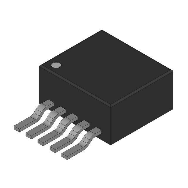
TO-220, TO-263 and SOIC-8 Packages
Over Temperature/Over Current Protection
−40°C to +125°C Junction Temperature Range
APPLICATIONS
•
•
•
•
•
•
•
DSP Power Supplies
Server Core and I/O Supplies
PC Add-in-Cards
Local Regulators in Set-Top Boxes
Microcontroller Power Supplies
High Efficiency Power Supplies
SMPS Post-Regulators
The fast transient response of these devices makes
them suitable for use in powering DSP,
Microcontroller Core voltages and Switch Mode
Power Supply post regulators. The parts are available
in TO-220, TO-263 and SOIC-8 packages.
Dropout Voltage: 75 mV (typ) @ 0.8A load current.
Ground Pin Current: 3 mA (typ) at full load.
Shutdown Current: 60 nA (typ) when S/D pin is low.
Precision Output Voltage: 1.5% room temperature
accuracy.
TYPICAL APPLICATION CIRCUIT
At least 4.7 µF of input and output capacitance is required for stability.
1
2
Please be aware that an important notice concerning availability, standard warranty, and use in critical applications of
Texas Instruments semiconductor products and disclaimers thereto appears at the end of this data sheet.
All trademarks are the property of their respective owners.
PRODUCTION DATA information is current as of publication date.
Products conform to specifications per the terms of the Texas
Instruments standard warranty. Production processing does not
necessarily include testing of all parameters.
Copyright © 2003–2013, Texas Instruments Incorporated
�LP3881
SNVS224F – MARCH 2003 – REVISED APRIL 2013
www.ti.com
Connection Diagrams
Figure 1. TO-220, Top View
Figure 2. TO-263, Top View
VOUT 1
VOUT 2
VBIAS 3
GND 4
GND
8 N/C
7 VIN
6 S/D
5 GND
Figure 3. SOIC-8, Top View
.
.
Block Diagram
These devices have limited built-in ESD protection. The leads should be shorted together or the device placed in conductive foam
during storage or handling to prevent electrostatic damage to the MOS gates.
2
Submit Documentation Feedback
Copyright © 2003–2013, Texas Instruments Incorporated
Product Folder Links: LP3881
�LP3881
www.ti.com
SNVS224F – MARCH 2003 – REVISED APRIL 2013
ABSOLUTE MAXIMUM RATINGS
(1)
−65°C to +150°C
Storage Temperature Range
Lead Temp. (Soldering, 5 seconds)
ESD Rating
260°C
Human Body Model (2)
2 kV
Machine Model (3)
Power Dissipation (4)
200V
Internally Limited
VIN Supply Voltage (Survival)
−0.3V to +6V
VBIAS Supply Voltage (Survival)
−0.3V to +7V
−0.3V to +7V
Shutdown Input Voltage (Survival)
IOUT (Survival)
Internally Limited
−0.3V to +6V
Output Voltage (Survival)
−40°C to +150°C
Junction Temperature
(1)
(2)
(3)
(4)
Absolute maximum ratings indicate limits beyond which damage to the component may occur. Operating ratings indicate conditions for
which the device is intended to be functional, but do not ensure specific performance limits. For ensured specifications, see Electrical
Characteristics. Specifications do not apply when operating the device outside of its rated operating conditions.
The human body model is a 100 pF capacitor discharged through a 1.5k resistor into each pin.
The machine model is a 220 pF capacitor discharged directly into each pin. The machine model ESD rating of pin 5 is 100V.
At elevated temperatures, device power dissipation must be derated based on package thermal resistance and heatsink thermal values.
θJ-A for TO-220 devices is 65°C/W if no heatsink is used. If the TO-220 device is attached to a heatsink, a θJ-S value of 4°C/W can be
assumed. θJ-A for TO-263 devices is approximately 40°C/W if soldered down to a copper plane which is at least 1.5 square inches in
area. θJ-A value for typical SOIC-8 PC board mounting is 166°C/W. If power dissipation causes the junction temperature to exceed
specified limits, the device will go into thermal shutdown.
OPERATING RATINGS
VIN Supply Voltage
(VOUT + VDO) to 5.5V
Shutdown Input Voltage
0 to +6V
IOUT
0.8A
−40°C to +125°C
Operating Junction Temperature Range
VBIAS Supply Voltage
4.5V to 6V
Submit Documentation Feedback
Copyright © 2003–2013, Texas Instruments Incorporated
Product Folder Links: LP3881
3
�LP3881
SNVS224F – MARCH 2003 – REVISED APRIL 2013
www.ti.com
ELECTRICAL CHARACTERISTICS
Limits in standard typeface are for TJ = 25°C, and limits in boldface type apply over the full operating temperature range.
Unless otherwise specified: VIN = VO(NOM) + 1V, VBIAS = 4.5V, IL = 10 mA, CIN = COUT = 4.7 µF, VS/D = VBIAS.
Symbol
VO
Parameter
Conditions
Output Voltage Tolerance
10 mA < IL < 0.8A
VO(NOM) + 1V ≤ VIN ≤ 5.5V
4.5V ≤ VBIAS ≤ 6V
Min (1)
Typical (2)
1.198
Max (1)
Units
1.234
1.216
1.186
1.246
1.478
1.522
1.5
1.455
V
1.545
1.773
1.827
1.8
1.746
(3)
1.854
ΔVO/ΔVIN
Output Voltage Line Regulation
VO(NOM) + 1V ≤ VIN ≤ 5.5V
0.01
%/V
ΔVO/ΔIL
Output Voltage Load Regulation (4)
10 mA < IL < 0.8A
0.04
0.06
%/A
VDO
Dropout Voltage (5)
IL = 0.8A
(TO220 and TO263 only)
75
120
160
IL = 0.8A
(SOIC only)
80
140
190
10 mA < IL < 0.8A
3
7
8
mA
0.03
1
30
µA
1
2
3
mA
VS/D ≤ 0.3V
0.03
1
30
µA
VOUT = 0V
2.5
IQ(VIN)
Quiescent Current Drawn from VIN
Supply
VS/D ≤ 0.3V
IQ(VBIAS)
ISC
Quiescent Current Drawn from
VBIAS Supply
Short-Circuit Current
10 mA < IL < 0.8A
mV
A
Shutdown Input
VSDT
Output Turn-off Threshold
Output = ON
1.3
0.7
Output = OFF
0.7
Td (OFF)
Turn-OFF Delay
RLOAD X COUT
很抱歉,暂时无法提供与“LP3881ES-1.8/NOPB”相匹配的价格&库存,您可以联系我们找货
免费人工找货