LP3882ES-1.2/NOPB

LP3882ES-1.2/NOPB

  • 厂商:

    BURR-BROWN(德州仪器)

  • 封装:

    TO263-6

  • 描述:

    1.5A 快速响应超低压降线性稳压器 5-DDPAK/TO-263 -40 to 125

  • 详情介绍
  • 数据手册
  • 价格&库存
LP3882ES-1.2/NOPB 数据手册
LP3882 www.ti.com SNVS226F – MARCH 2003 – REVISED APRIL 2013 LP3882 1.5A Fast-Response Ultra Low Dropout Linear Regulators Check for Samples: LP3882 FEATURES DESCRIPTION • The LP3882 is a high current, fast response regulator which can maintain output voltage regulation with minimum input to output voltage drop. Fabricated on a CMOS process, the device operates from two input voltages: Vbias provides voltage to drive the gate of the N-MOS power transistor, while Vin is the input voltage which supplies power to the load. The use of an external bias rail allows the part to operate from ultra low Vin voltages. Unlike bipolar regulators, the CMOS architecture consumes extremely low quiescent current at any output load current. The use of an N-MOS power transistor results in wide bandwidth, yet minimum external capacitance is required to maintain loop stability. 1 2 • • • • • • • Ultra Low Dropout Voltage (110 mV at 1.5A typ) Low Ground Pin Current Load Regulation of 0.04%/A 60 nA Typical Quiescent Current in Shutdown 1.5% Output Accuracy (25°C) TO-220, DDPAK/TO-263 and SO PowerPad Packages Over Temperature/Over Current Protection −40°C to +125°C Junction Temperature Range APPLICATIONS • • • • • • • DSP Power Supplies Server Core and I/O Supplies PC Add-in-Cards Local Regulators in Set-Top Boxes Microcontroller Power Supplies High Efficiency Power Supplies SMPS Post-Regulators The fast transient response of these devices makes them suitable for use in powering DSP, Microcontroller Core voltages and Switch Mode Power Supply post regulators. The parts are available in TO-220, DDPAK/TO-263 and SO PowerPad packages. Dropout Voltage: 110 mV (typ) at 1.5A load current. Ground Pin Current: 3 mA (typ) at full load. Shutdown Current: 60 nA (typ) when S/D pin is low. Precision Output Voltage: 1.5% room temperature accuracy. TYPICAL APPLICATION CIRCUIT At least 4.7 µF of input and output capacitance is required for stability. 1 2 Please be aware that an important notice concerning availability, standard warranty, and use in critical applications of Texas Instruments semiconductor products and disclaimers thereto appears at the end of this data sheet. All trademarks are the property of their respective owners. PRODUCTION DATA information is current as of publication date. Products conform to specifications per the terms of the Texas Instruments standard warranty. Production processing does not necessarily include testing of all parameters. Copyright © 2003–2013, Texas Instruments Incorporated LP3882 SNVS226F – MARCH 2003 – REVISED APRIL 2013 www.ti.com These devices have limited built-in ESD protection. The leads should be shorted together or the device placed in conductive foam during storage or handling to prevent electrostatic damage to the MOS gates. CONNECTION DIAGRAM Figure 1. 5-Pin TO-220, Top View See NDH0005D Package Figure 2. 5-Pin DDPAK/TO-263, Top View See KTT0005B Package VOUT 1 VOUT 2 VBIAS 3 GND 4 GND 8 N/C 7 VIN 6 S/D 5 GND Figure 3. 8-Pin SO PowerPad, Top View See DDA0008D Package White Space White Space White Space BLOCK DIAGRAM 2 Submit Documentation Feedback Copyright © 2003–2013, Texas Instruments Incorporated Product Folder Links: LP3882 LP3882 www.ti.com SNVS226F – MARCH 2003 – REVISED APRIL 2013 ABSOLUTE MAXIMUM RATINGS (1) If Military/Aerospace specified devices are required, contact the Texas Instruments Semiconductor Sales Office/ Distributors for availability and specifications. VALUE / UNITS −65°C to +150°C Storage Temperature Range Lead Temperature (Soldering, 5 seconds) ESD Rating Human Body Model Machine Model Power Dissipation 260°C (2) 2 kV (3) 200V (4) Internally Limited VIN Supply Voltage (Survival) −0.3V to +6V VBIAS Supply Voltage (Survival) −0.3V to +7V Shutdown Input Voltage (Survival) −0.3V to +7V IOUT (Survival) Internally Limited Output Voltage (Survival) (5) −0.3V to +6V −40°C to +150°C Junction Temperature (1) (2) (3) (4) (5) Absolute maximum ratings indicate limits beyond which damage to the component may occur. Operating ratings indicate conditions for which the device is intended to be functional, but does not ensure specific performance limits. For specifications, see Electrical Characteristics. Specifications do not apply when operating the device outside of its rated operating conditions. The human body model is a 100 pF capacitor discharged through a 1.5k resistor into each pin. The machine model is a 220 pF capacitor discharged directly into each pin. The machine model ESD rating of pin 5 is 100V. At elevated temperatures, device power dissipation must be derated based on package thermal resistance and heatsink thermal values. θJ-A for TO-220 devices is 65°C/W if no heatsink is used. If the TO-220 device is attached to a heatsink, a θJ-S value of 4°C/W can be assumed. θJ-A for DDPAK/TO-263 devices is approximately 40°C/W if soldered down to a copper plane which is at least 1.5 square inches in area. θJ-A value for typical SO PowerPad PC board mounting is 166°C/W. If power dissipation causes the junction temperature to exceed specified limits, the device will go into thermal shutdown. If used in a dual-supply system where the regulator load is returned to a negative supply, the output pin must be diode clamped to ground. RECOMMENDED OPERATING CONDITIONS VALUE / UNITS VIN Supply Voltage (VOUT + VDO) to 5.5V Shutdown Input Voltage 0 to +6V IOUT Operating Junction 1.5A −40°C to +125°C Temperature Range VBIAS Supply Voltage 4.5V to 6V Submit Documentation Feedback Copyright © 2003–2013, Texas Instruments Incorporated Product Folder Links: LP3882 3 LP3882 SNVS226F – MARCH 2003 – REVISED APRIL 2013 www.ti.com ELECTRICAL CHARACTERISTICS Limits in standard typeface are for TJ = 25°C, and limits in boldface type apply over the full operating temperature range. Unless otherwise specified: VIN = VO(NOM) + 1V, VBIAS = 4.5V, IL = 10 mA, CIN = COUT = 4.7 µF, VS/D = VBIAS. Symbol VO Parameter Conditions Output Voltage Tolerance ΔVO/ΔVIN Output Voltage Line Regulation ΔVO/ΔIL Output Voltage Load Regulation VDO Dropout Voltage IQ(VIN) MIN 10 mA < IL < 1.5A VO(NOM) + 1V ≤ VIN ≤ 5.5V 4.5V ≤ VBIAS ≤ 6V (3) (4) (5) Quiescent Current Drawn from VIN Supply (1) ISC Quiescent Current Drawn from VBIAS Supply Short-Circuit Current (2) MAX (1) 1.198 1.186 1.216 1.234 1.246 1.478 1.455 1.5 1.522 1.545 1.773 1.746 1.8 1.827 1.854 Units V VO(NOM) + 1V ≤ VIN ≤ 5.5V 0.01 %/V 10 mA < IL < 1.5A 0.04 0.06 %/A IL = 1.5A (TO-220 and DDPAK/TO-263 only) 110 170 270 IL = 1.5A (PSOP only) 125 190 320 3 7 8 mA 0.03 1 30 µA 1 2 3 mA VS/D ≤ 0.3V 0.03 1 30 µA VOUT = 0V 4.3 10 mA < IL < 1.5A VS/D ≤ 0.3V IQ(VBIAS) Typical 10 mA < IL < 1.5A mV A Shutdown Input VSDT Output Turn-off Threshold Output = ON 1.3 0.7 Output = OFF 0.7 Td (OFF) Turn-OFF Delay RLOAD X COUT
LP3882ES-1.2/NOPB
物料型号:LP3882 器件简介:LP3882是一款高电流、快速响应的低压降线性调节器,能够在极低的输入至输出电压降下维持输出电压的稳定。

该器件在CMOS工艺上制造,使用两个输入电压:Vbias为N-MOS功率晶体管的栅极提供电压,而Vin则是供给负载的输入电压。

它可以使用外部偏置轨在超低Vin电压下工作。

与双极型调节器不同,CMOS架构在任何输出负载电流下都消耗极低的静态电流。

使用N-MOS功率晶体管可以获得宽带宽,同时只需要极少的外部电容以维持环路稳定性。

引脚分配: - 
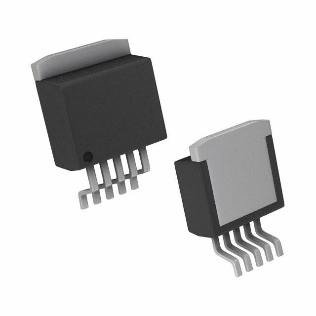
5-Pin TO-220: GND, BIAS, OUTPUT, INPUT, SHUTDOWN - 5-Pin DDPAK/TO-263: GND, BIAS, OUTPUT, INPUT, SHUTDOWN - 8-Pin SO PowerPad: VIN, VOUT, GND, S/D, VBIAS, GND, GND, NC 参数特性: - 超低 dropout 电压:110 mV(1.5A时典型值) - 负载调节:0.04%/A - 关闭时的典型静态电流:60 nA - 输出精度:1.5%(在25°C时) - 工作结温范围:-40°C至+125°C 功能详解: - LP3882具有快速瞬态响应,适合用于数字信号处理器(DSP)、微控制器核心电压和开关模式电源(SMPS)后级调节器的供电。

- 提供过温和过流保护。

应用信息: - DSP电源 - 服务器核心和I/O电源 - 计算机插件卡 - 机顶盒中的局部调节器 - 微控制器电源 封装信息: - TO-220, DDPAK/TO-263 和 SO PowerPad 封装

以上信息摘自德州仪器公司发布的LP3882数据手册。
LP3882ES-1.2/NOPB 价格&库存

很抱歉,暂时无法提供与“LP3882ES-1.2/NOPB”相匹配的价格&库存,您可以联系我们找货

免费人工找货
LP3882ES-1.2/NOPB
  •  国内价格 香港价格
  • 1+58.564421+7.53638

库存:0

LP3882ES-1.2/NOPB
  •  国内价格
  • 1+61.96070
  • 100+51.63400
  • 250+41.30710
  • 1000+34.42260

库存:0