User's Guide
SNVA650A – May 2012 – Revised April 2013
AN-2261 LP38869EVAL - 1A FlexCap LDO
1
Introduction
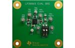
The LP38869EVAL evaluation board is designed to demonstrate the capabilities of the LP38869MH high
performance LDO voltage regulator. It is intended to provide a flexible circuit configuration and access to
points of interest. The circuit schematic is shown in Figure 8.
Component placement is shown in Figure 2 and Figure 3. The PCB layout is shown in Figure 5 through
Figure 7. Test points are provided on the evaluation board for signal monitoring.
2
Operating Range
•
•
•
•
•
•
3
Minimum Operating Input Voltage: 2.70V (For 2.50V Pre-Set VOUT)
Maximum Operating Input Voltage: 5.50V
Output Voltage : 2.50V (Pre-Set Mode) or 3.30V (Adjustable Mode), selectable via SW1-1
Maximum Operating Output Current: 1A
Ambient Temperature Operating Range: 0°C to 50°C
Board Size: 1.90 inches x 2.00 inches
Evaluation Board Start-Up
Before applying power to the LP38869EVAL board, all external connections should be verified. The
external power supply must be turned off before being connected. Confirm proper polarity to the 'VIN'
(TP1) and 'GND' (TP2) terminals before turning the external power supply on. An appropriate load should
be connected between the 'VOUT1' (TP3) and 'GND'(TP5) terminals. Under basic evaluation conditions
the test points TP4 (VOUT2), TP6 (/RST), TP7 (SS), and TP8 (SET) can be left open. The two switches
(SW1-1, and SW1-2) should be in the OFF positions (i.e., switch levers are towards the TI logo). The
evaluation board will be in the normal operating mode when input power is applied.
4
SHDN
Normal operation is when SW1-2 is in the OFF position (i.e. the switch lever is towards the TI logo at the
bottom edge of the board). Moving SW1-2 to the ON position will connect the SHDN pin to ground which
will disable the output. There is no Test Point for the SHDN pin. See Figure 4.
5
Soft-Start
Unlike traditional Soft-Start circuits that slow the rise time of the output voltage, the LP38869 Soft-Start
circuit slowly increases the available output current. The rise time is controlled by the value of the SS
capacitor (C3). The maximum output current can also be limited by placing a resistor in parallel with the
SS capacitor, from TP7 to Ground. See the LP38869 datasheet for more details
All trademarks are the property of their respective owners.
SNVA650A – May 2012 – Revised April 2013
Submit Documentation Feedback
AN-2261 LP38869EVAL - 1A FlexCap LDO
Copyright © 2012–2013, Texas Instruments Incorporated
1
�Output Voltage Selection
6
www.ti.com
Output Voltage Selection
Normal operation is when SW1-1 is in the OFF position (i.e. the switch lever is towards the TI logo at the
bottom edge of the board). With SW1-1 in the OFF position the output voltage will be determined by the
internal settings (i.e., 2.50V). Moving SW1-1 to the ON position will connect the LP38869 OUT pin to the
SET pin through resistors R3 and R4 which will disable the internally set output voltage (2.50V), and will
use the external resistors (R2, R3, and R4) to set the output voltage to the adjustable value of 3.30V. See
Figure 4.
6.1
Changing the Output Voltage
The LP38869EVAL board is assembled with R3= 0.0Ω, R4= 31.6 kΩ and R2= 10.0 kΩ, to set the typical
output voltage to 3.30V when SW1-1 is in the ON position.
Resistors R2, R3, and R4 may be replaced, as needed, to achieve the desired output voltage as long as
the value for R3 and R4 is low enough so that the SET pin bias current flowing through R3 and R4 does
not cause any offset in the output voltage.
The following formula is used to determine the typical output voltage:
VOUT = (VSET x (1 + (R4 / R2) )) + (ISET x R4)
(1)
Keeping the value for R4 less than about 100 kΩ will minimize the effects of ISET and the formula can be
simplified to the traditional:
VOUT = (VSET x (1 + (R4 / R2) ))
(2)
For the resistors installed on the LP38869EVAL board:
VOUT= ( 0.8V x ( 1 + (31.6 kΩ / 10.0 kΩ) ) = 3.328V (typical)
(3)
Alternately, the following formula can be used to determine the appropriate R4 value for a given R2 value
with a VOUT ≥ 0.800V:
R1= ( ( ( VOUT / VSET ) - 1) x R4 )
(4)
The following table suggests some ±1% tolerance values for R4, keeping R2 and R3 held at the installed
values of 10.0 k Ω and 0Ω respectively, for a range of output voltages using the typical VSET value of 800
mV. This is not a definitive list, as other combinations R2 and R4 do exist that will provide similar, possibly
better, performance.
Target VOUT
R4
R2
Typical VOUT
1.00V
2.49 kΩ
10.0 kΩ
0.999V
1.80V
12.4 kΩ
10.0 kΩ
1.792V
21.5 kΩ
10.0 kΩ
2.52V
Open
10.0 kΩ
2.50V
3.30V
31.6 kΩ
10.0 kΩ
3.32V
5.00V
52.3 kΩ
10.0 kΩ
4.98V
2.50V
2
AN-2261 LP38869EVAL - 1A FlexCap LDO
Copyright © 2012–2013, Texas Instruments Incorporated
SNVA650A – May 2012 – Revised April 2013
Submit Documentation Feedback
�Output Voltage Selection
www.ti.com
In the Adjustable Mode the resistors used for R4 and R2 should be high quality, tight tolerance, and with
matching temperature coefficients. It is important to remember that, although the value of VREF is ensured,
the final value of VOUT in the Adjustable Mode is not. The use of low quality resistors for R4 and R2 can
easily produce an Adjustable Mode VOUT value that is unacceptable.
N/C
1
16
N/C
IN
2
15
OUT
IN
3
14
OUT
IN
4
13
OUT
IN
5
12
OUT
RST
6
11
SET
SHDN
7
10
GND
SS
8
9
N/C
Exposed Pad
on Bottom
(DAP)
Figure 1. LP38869MH (16 Pin TSSOP-EP) Connection Diagram
Figure 2. Top Side Parts Placement, as Viewed from the Top
Figure 3. Bottom Side Part Placement, as Viewed from the Top
SNVA650A – May 2012 – Revised April 2013
Submit Documentation Feedback
AN-2261 LP38869EVAL - 1A FlexCap LDO
Copyright © 2012–2013, Texas Instruments Incorporated
3
�Output Voltage Selection
www.ti.com
VOUT
Adjustable
VOUT
OFF
ON
SW1-2
SW1-1
VOUT
Pre-Set
1
2
VOUT
ON
SW1
Figure 4. SW1-1 and SW1-2 Functions
Figure 5. Top Layer as Viewed from Top
Figure 6. Copper Layer 1 (Top Layer) as Viewed from Top
Figure 7. Copper Layer 2 (Bottom Layer) as Viewed from Top
4
AN-2261 LP38869EVAL - 1A FlexCap LDO
Copyright © 2012–2013, Texas Instruments Incorporated
SNVA650A – May 2012 – Revised April 2013
Submit Documentation Feedback
�Schematic for LP38869EVAL
www.ti.com
7
Schematic for LP38869EVAL
1
R1
100k
2
TP1
VIN
3
4
N/C
IN
OUT
IN
OUT
IN
OUT
16
15
TP3
VOUT1
R3
0.0
14
TP4
VOUT2
13
R4
31.6k
LP38869MH
R5
1M
5
6
TP6
/RST
7
SW1-2
TP7
SS
N/C
C1
1 uF
8
IN
OUT
RST
SET
SHDN
GND
SW1-1
11
SS
C3
0.1 uF
TP2
GND
12
10
C2
1 uF
9
R6
0.0
N/C
DAP
R2
10.0k
TP5
GND
Figure 8. LP38869EVAL Schematic
Table 1. Bill of Materials for LP38869EVAL
Description
Manufacturer
Manufacturer
Part Number
Digi-Key
Number
U1
Voltage Regulator, LDO
Texas Instruments
LP38869MH
-
C1, C2
Capacitor: MLCC, 1µF, 25V, +/10%, X7R, 0805
TDK
C2012X7R1E105K
445-1354-1-ND
C3
Capacitor: MLCC, 0.1µF, 25V,
+/-10%, X7R, 0805
MuRata
GRM21BR71E104KA01L
490-1673-1-ND
R1
Resistor: 100 kΩ, 1%, 0.125W,
0805
Panasonic
ERJ-6ENF1003V
P100KCCT-ND
R2
Resistor: 10.0 kΩ, 1%, 0.125W,
0805
Panasonic
ERJ-6ENF1002V
P10.0KCCT-ND
R3
Resistor: 0.0Ω, 0.125W, 0805
Vishay-Dale
CRCW08050000Z0EA
541-0.0ACT-ND
R4
Resistor: 31.6 kΩ, 1%, 0.125W,
0805
Panasonic
ERJ-6ENF3162V
P31.6KCCT-ND
R5
Resistor: 1.00 M Ω, 1%,
0.125W, 0805
Vishay-Dale
CRCW08051M00FKEA
541-1.00MCCT-ND
R6
Resistor: 0 Ω, 5%, 0.063W,
0402
Panasonic
ERJ-2GE0R00X
P0.0JCT-ND
SW1
Switch: DIP, Top Slide, 2
Position, SPST, SMD
C&K
SDA02H1SBD
CKN6056-ND
TP1, TP2, TP3,
TP4, TP5, TP8
Terminal: Turret, TH, Double
Keystone
1502-2
1502-2K-ND
TP6, TP7
Test Point: TH, Miniature, White
Keystone
5002
5002K-ND
Designator
SNVA650A – May 2012 – Revised April 2013
Submit Documentation Feedback
AN-2261 LP38869EVAL - 1A FlexCap LDO
Copyright © 2012–2013, Texas Instruments Incorporated
5
�Schematic for LP38869EVAL
6
www.ti.com
AN-2261 LP38869EVAL - 1A FlexCap LDO
Copyright © 2012–2013, Texas Instruments Incorporated
SNVA650A – May 2012 – Revised April 2013
Submit Documentation Feedback
�IMPORTANT NOTICE
Texas Instruments Incorporated and its subsidiaries (TI) reserve the right to make corrections, enhancements, improvements and other
changes to its semiconductor products and services per JESD46, latest issue, and to discontinue any product or service per JESD48, latest
issue. Buyers should obtain the latest relevant information before placing orders and should verify that such information is current and
complete. All semiconductor products (also referred to herein as “components”) are sold subject to TI’s terms and conditions of sale
supplied at the time of order acknowledgment.
TI warrants performance of its components to the specifications applicable at the time of sale, in accordance with the warranty in TI’s terms
and conditions of sale of semiconductor products. Testing and other quality control techniques are used to the extent TI deems necessary
to support this warranty. Except where mandated by applicable law, testing of all parameters of each component is not necessarily
performed.
TI assumes no liability for applications assistance or the design of Buyers’ products. Buyers are responsible for their products and
applications using TI components. To minimize the risks associated with Buyers’ products and applications, Buyers should provide
adequate design and operating safeguards.
TI does not warrant or represent that any license, either express or implied, is granted under any patent right, copyright, mask work right, or
other intellectual property right relating to any combination, machine, or process in which TI components or services are used. Information
published by TI regarding third-party products or services does not constitute a license to use such products or services or a warranty or
endorsement thereof. Use of such information may require a license from a third party under the patents or other intellectual property of the
third party, or a license from TI under the patents or other intellectual property of TI.
Reproduction of significant portions of TI information in TI data books or data sheets is permissible only if reproduction is without alteration
and is accompanied by all associated warranties, conditions, limitations, and notices. TI is not responsible or liable for such altered
documentation. Information of third parties may be subject to additional restrictions.
Resale of TI components or services with statements different from or beyond the parameters stated by TI for that component or service
voids all express and any implied warranties for the associated TI component or service and is an unfair and deceptive business practice.
TI is not responsible or liable for any such statements.
Buyer acknowledges and agrees that it is solely responsible for compliance with all legal, regulatory and safety-related requirements
concerning its products, and any use of TI components in its applications, notwithstanding any applications-related information or support
that may be provided by TI. Buyer represents and agrees that it has all the necessary expertise to create and implement safeguards which
anticipate dangerous consequences of failures, monitor failures and their consequences, lessen the likelihood of failures that might cause
harm and take appropriate remedial actions. Buyer will fully indemnify TI and its representatives against any damages arising out of the use
of any TI components in safety-critical applications.
In some cases, TI components may be promoted specifically to facilitate safety-related applications. With such components, TI’s goal is to
help enable customers to design and create their own end-product solutions that meet applicable functional safety standards and
requirements. Nonetheless, such components are subject to these terms.
No TI components are authorized for use in FDA Class III (or similar life-critical medical equipment) unless authorized officers of the parties
have executed a special agreement specifically governing such use.
Only those TI components which TI has specifically designated as military grade or “enhanced plastic” are designed and intended for use in
military/aerospace applications or environments. Buyer acknowledges and agrees that any military or aerospace use of TI components
which have not been so designated is solely at the Buyer's risk, and that Buyer is solely responsible for compliance with all legal and
regulatory requirements in connection with such use.
TI has specifically designated certain components as meeting ISO/TS16949 requirements, mainly for automotive use. In any case of use of
non-designated products, TI will not be responsible for any failure to meet ISO/TS16949.
Products
Applications
Audio
www.ti.com/audio
Automotive and Transportation
www.ti.com/automotive
Amplifiers
amplifier.ti.com
Communications and Telecom
www.ti.com/communications
Data Converters
dataconverter.ti.com
Computers and Peripherals
www.ti.com/computers
DLP® Products
www.dlp.com
Consumer Electronics
www.ti.com/consumer-apps
DSP
dsp.ti.com
Energy and Lighting
www.ti.com/energy
Clocks and Timers
www.ti.com/clocks
Industrial
www.ti.com/industrial
Interface
interface.ti.com
Medical
www.ti.com/medical
Logic
logic.ti.com
Security
www.ti.com/security
Power Mgmt
power.ti.com
Space, Avionics and Defense
www.ti.com/space-avionics-defense
Microcontrollers
microcontroller.ti.com
Video and Imaging
www.ti.com/video
RFID
www.ti-rfid.com
OMAP Applications Processors
www.ti.com/omap
TI E2E Community
e2e.ti.com
Wireless Connectivity
www.ti.com/wirelessconnectivity
Mailing Address: Texas Instruments, Post Office Box 655303, Dallas, Texas 75265
Copyright © 2013, Texas Instruments Incorporated
�