LP3936
www.ti.com
SNVS259D – NOVEMBER 2003 – REVISED MAY 2013
LP3936 Lighting Management System for Six White LEDs and One RGB or FLASH LED
Check for Samples: LP3936
FEATURES
APPLICATIONS
•
•
•
1
2
•
•
•
•
•
•
•
•
•
High Efficiency 250 mA Magnetic Boost DC-DC
Converter with Programmable Output Voltage
PWM controlled RGB LED drivers with
programmable color, brightness, turn on/off
slopes and blinking
FLASH function with 3 drivers, each up to 120
mA current
4 constant current White LED drivers with
programmable 8-bit adjustment
(0 … 25 mA/LED)
2 constant current White LED drivers with
programmable 8-bit adjustment
(0 … 25 mA/LED)
8-bit ADC for ambient light sensor with
averaging
Combined MicroWire/SPI and I2C compatible
serial interface
Low current Standby mode (software
controlled)
Low voltage digital interface down to 1.8V
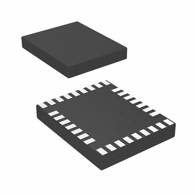
Space efficient 32-pin TLGA laminate package
Cellular Phones
PDAs
DESCRIPTION
LP3936 is a complete lighting management system
designed for portable wireless applications. It
contains a boost DC/DC converter, 4 white LED
drivers to drive the main LCD panel backlight, 2 white
LED drivers for sub-LCD panel and 1 set of RGB
LED drivers.
Both WLED groups have 8-bit programmable
constant current drivers that are separately adjustable
and matched to 1% (typ.). For efficient backlighting
the backlight intensity can be adjusted using the 8-bit
ADC with ambient light detection circuit.
The RGB LED drivers are PWM-driven with
programmable color, intensity and blinking patterns.
In addition, they feature a FLASH function to support
picture taking with camera-enabled cellular phones.
Typical Application
D1
L1
10 PH
Li-Ion Battery
or Charger
V IN
+
VDD
CIN
OUT
10 PF
V OUT =
4.1 - 5.3V
FB
WLED1
WLED2
4
Baseband
Processor
or
Microcontroller
I2C or
MicroWire/
SPI Interface
MW_SEL
RGB_EN
IMAX = 250 mA
WLED3
COUT
10 PF
Main Display
Backlight
0 - 25 mA
per LED
WLED4
LP3936
NRST
WLED5
WLED6
V DD_IO
Optical
sensor
AIN
Sub Display
Backlight
0 - 25 mA
per LED
ROUT
RGB
GOUT
120 mA
max. per
LED
BOUT
AREF
GND
1
2
Please be aware that an important notice concerning availability, standard warranty, and use in critical applications of
Texas Instruments semiconductor products and disclaimers thereto appears at the end of this data sheet.
All trademarks are the property of their respective owners.
PRODUCTION DATA information is current as of publication date.
Products conform to specifications per the terms of the Texas
Instruments standard warranty. Production processing does not
necessarily include testing of all parameters.
Copyright © 2003–2013, Texas Instruments Incorporated
�LP3936
SNVS259D – NOVEMBER 2003 – REVISED MAY 2013
www.ti.com
DESCRIPTION (CONTINUED)
An efficient magnetic boost converter provides the required bias operating from a single Li-Ion battery. The
DC/DC converter output voltage is user programmable for adapting to different LED types and for efficiency
optimization. All functions are software controllable through an I2C and MicroWire/SPI compatible interface and
16 internal registers.
Connection Diagrams and Package Mark Information
GND_BOOST
4
GND2
5
WLED1
SCL
SCL
WLED4
8
18
VREF
9
10 11 12 13 14 15 16 17
19
7
WLED3
VREF
18
8
WLED4
17 16 15 14 13 12 11 10
9
GND_T
AIN
AREF
VDD1
GND1
VDDA
WLED6
WLED2
RT
Figure 1. TLGA Package – Top View
See Package Number NPC0032A
GND_WLED
RT
6
LP3936
WLED5
19
21
20
WLED6
7
NRST
GND1
WLED3
FB
MW_SEL
VDDA
MW_SEL
VDD1
NRST
20
LP3936
AIN
21
6
GND_T
5
WLED2
AREF
VDD_IO
4
WLED5
ROUT
GND2
WLED1
GND_WLED
RGB_EN
CS
GOUT
CS
GND_RGB
22
BOUT
3
DO
GND_RGB
VDD2
22
DI
23
BOUT
3
24
GOUT
2
23
2
VDD_IO
24
32 31 30 29 28 27 26 25
ROUT
DI
DO
1
RGB_EN
1
OUT
25 26 27 28 29 30 31 32
GND_BOOST
FB
VDD2
OUT
32-Lead TLGA Package, 4.5 x 5.5 x 0.8 mm, 0.5 mm pitch
Figure 2. TLGA Package – Bottom View
Pin Description
2
Pin
Name
Type
1
GND_BOOST
Ground
Description
Power Switch Ground
2
FB
Input
3
VDD2
Power
Boost Converter Feedback
Supply Voltage for Internal Digital Circuits
Ground Return for VDD2 (Internal Digital)
4
GND2
Ground
5
WLED1
LED Output
Open Drain, White LED1 Output
6
WLED2
LED Output
Open Drain, White LED2 Output
7
WLED3
LED Output
Open Drain, White LED3 Output
8
WLED4
LED Output
Open Drain, White LED4 Output
9
GND_WLED
Ground
10
WLED5
LED Output
Open Drain, White LED5 Output
11
WLED6
LED Output
Open Drain, White LED6 Output
12
VDDA
Output
Internal LDO Output, 2.8V
13
GND1
Ground
Ground Return for VDD1 (Internal Analog)
14
VDD1
Power
Supply Voltage for Internal Analog Circuits
15
AIN
Input
16
AREF
Output
Reference Voltage for Ambient Light Sensor, 1.23V
17
GND_T
Ground
Ground
18
VREF
Output
Internal Reference Bypass Capacitor
19
RT
Input
20
MW_SEL
Logic Input
4+2 White LED Driver Ground
Ambient Light Sensor Input
Oscillator Resistor
MicroWire — I2C select (MW_SEL=1 in MicroWire Mode)
Submit Documentation Feedback
Copyright © 2003–2013, Texas Instruments Incorporated
Product Folder Links: LP3936
�LP3936
www.ti.com
SNVS259D – NOVEMBER 2003 – REVISED MAY 2013
Pin Description (continued)
Pin
Name
Type
21
NRST
Logic Input
Description
22
CS
Logic Input/Output
23
DO
Logic Output
24
DI
Logic Input
MicroWire Data Input
25
SCL
Logic Input
MicroWire Clock / I2C SCL Input
26
RGB_EN
Logic Input
LED Control for On/Off or PWM Dimming
27
VDD_IO
Power
28
ROUT
LED Output
Open Drain Output, Red LED
29
GOUT
LED Output
Open Drain Output, Green LED
30
BOUT
LED Output
Open Drain Output, Blue LED
31
GND_RGB
Ground
Ground for RGB Drivers
32
OUT
Output
Open Drain, Boost Converter Power Switch
Low Active Reset Input
MicroWire Chip-Select (in) / I2C SDA (in/out)
MicroWire Data Output
Supply Voltage for Logic IO signals
These devices have limited built-in ESD protection. The leads should be shorted together or the device placed in conductive foam
during storage or handling to prevent electrostatic damage to the MOS gates.
Absolute Maximum Ratings (1) (2) (3)
VDD1, VDD2, VDD_IO, V(OUT, FB)
-0.3V to 6.0V
Voltage on Logic Pins
-0.3V to VDD_IO + 0.3V, with 6.0V max
Voltage on LED Output Pins
-0.3V to V(FB) + 0.3V, with 6.0V max
Voltage on All Other Pins
-0.3V to VDD1,2 + 0.3V, with 6.0V max
I (ROUT, GOUT, BOUT)
150 mA
I (VREF)
10 µA
Continuous Power Dissipation (4)
Internally Limited
Junction Temperature (TJ-MAX)
125°C
−65°C to +150°C
Storage Temperature Range
Maximum Lead Temperature (Reflow soldering, 3 times) (5)
260°C
ESD Rating (6)
Human Body Model:
2 kV
Machine Model:
(1)
(2)
(3)
(4)
(5)
(6)
200V
All voltages are with respect to the potential at the GND pins (GND1, GND2, GND_T, GND_BOOST, GND_WLED, GND_RGB).
Absolute Maximum Ratings indicate limits beyond which damage to the component may occur. Operating Ratings are conditions under
which operation of the device is specified. Operating Ratings do not imply performance limits. For performance limits and associated test
conditions, see the Electrical Characteristics table.
If Military/Aerospace specified devices are required, please contact the Texas Instruments Sales Office / Distributors for
availability and specifications.
Internal thermal shutdown circuitry protects the device from permanent damage. Thermal shutdown engages at TJ = 160°C (typ.) and
disengages at TJ = 140°C (typ.).
For detailed soldering specifications and information, see TI's AN--1125 Application Report (SNAA002).
The Human body model is a 100 pF capacitor discharged through a 1.5 kΩ resistor into each pin. The machine model is a 200 pF
capacitor discharged directly into each pin. MIL-STD-883 3015.7
Operating Ratings (1) (2)
VDD1, VDD2
3.0V to 6.0V
VDD_IO
1.65V – VDD1,2
Recommended Load Current
0 mA to 250 mA
−40°C to +125°C
Junction Temperature (TJ) Range
(1)
(2)
Absolute Maximum Ratings indicate limits beyond which damage to the component may occur. Operating Ratings are conditions under
which operation of the device is specified. Operating Ratings do not imply performance limits. For performance limits and associated test
conditions, see the Electrical Characteristics table.
All voltages are with respect to the potential at the GND pins (GND1, GND2, GND_T, GND_BOOST, GND_WLED, GND_RGB).
Submit Documentation Feedback
Copyright © 2003–2013, Texas Instruments Incorporated
Product Folder Links: LP3936
3
�LP3936
SNVS259D – NOVEMBER 2003 – REVISED MAY 2013
www.ti.com
Operating Ratings(1)(2) (continued)
Ambient Temperature (TA) Range (3)
(3)
−40°C to +85°C
In applications where high power dissipation and/or poor package thermal resistance is present, the maximum ambient temperature may
have to be derated. Maximum ambient temperature (TA-MAX) is dependent on the maximum operating junction temperature (TJ-MAX-OP =
125°C), the maximum power dissipation of the device in the application (PD-MAX), and the junction-to ambient thermal resistance of the
part/package in the application (θJA), as given by the following equation:
TA-MAX = TJ-MAX-OP − (θJA x PD-MAX).
Thermal Characteristics
Junction-to-Ambient Thermal Resistance (θJA),
NPC0032A Package
(1)
4
(1)
72°C/W
Junction-to-ambient thermal resistance is highly application and board-layout dependent. In applications where high maximum power
dissipation exists, special care must be paid to thermal dissipation issues in board design.
Submit Documentation Feedback
Copyright © 2003–2013, Texas Instruments Incorporated
Product Folder Links: LP3936
�LP3936
www.ti.com
SNVS259D – NOVEMBER 2003 – REVISED MAY 2013
Electrical Characteristics (1) (2)
Limits in standard typeface are for TJ = 25°C. Limits in boldface type apply over the operating ambient temperature range
(−40°C ≤ TA ≤ +85°C). Unless otherwise noted, specifications apply to the Block Diagram with: VDD1 = VDD2 = VDD_IO = 3.6V,
CVDD1, CVDD2, CVDDIO = 1 µF, CIN, COUT = 10 µF, CVDDA = 1 µF, CVREF = 0.1 µF, LBOOST = 10 µH (3).
Symbol
Parameter
Min
Typ
Max
3.0
3.6
6.0
V
NSTBY = L (register)
CS, SCL, DI, NRST = H
VDD1, VDD2 = 3.6V
1
7
µA
No-Load Supply Current
(VDD1 and VDD2 current, boost off)
NSTBY = H (reg.)
EN_BOOST = L (reg.)
SCL, CS, DI, NRST = H
170
300
µA
Full Load Supply Current
(VDD1 and VDD2 current, boost on)
NSTBY = H (register)
NRST, CS, SCL, DI = H
RGB_EN = L
WLED1 … 6 = L
EN_AMBADC = L
1
mA
VDD_IO Standby Supply Current
NSTBY = L (register)
CS, SCL, DI, NRST = H
1
µA
VDD_IO Operating Supply Current
1 MHz Clock Frequency
CL = 50 pF at DO pin
20
µA
VDD1,2
Supply Voltage
IDD
Standby Supply Current
(VDD1 and VDD2 current)
IDD_IO
(4)
VREF
Reference Voltage
VDDA
LDO Output Voltage
(1)
(2)
(3)
(4)
Condition
Units
IREF ≤ 1 nA,
Test Purposes Only
1.205
−2
1.23
1.255
+2
V
%
IVDDA < 1 µA
2.688
–4
2.8
2.912
+4
%V
All voltages are with respect to the potential at the GND pins (GND1, GND2, GND_T, GND_BOOST, GND_WLED, GND_RGB).
Min and Max limits are specified by design, test, or statistical analysis. Typical numbers represent the most likely norm.
Low-ESR Surface-Mount Ceramic Capacitors (MLCCs) are used in setting electrical characteristics.
VREF pin (Bandgap reference output) is for internal use only. A capacitor should always be placed between VREF and GND1.
Submit Documentation Feedback
Copyright © 2003–2013, Texas Instruments Incorporated
Product Folder Links: LP3936
5
�LP3936
SNVS259D – NOVEMBER 2003 – REVISED MAY 2013
www.ti.com
BLOCK DIAGRAM
Li-Ion Battery
or Charger
V IN
C VDD1
C VDD2
C IN
1 PF
1 PF
10 PF
VDD1
L1
10 PH
VDD2
D1
VDDA
C VDDA
Boost Converter
LDO
2.8V / 1mA
1 PF
VREF
C VREF
Voltage
Reference
OUT
I MA = 250 mA
X
FB
V OUT =
4.1 - 5.3V
GND_BOOST
C OUT
ENABLE
10 PF
100 nF
RT
Main Display Backlight
Oscillator
WLED1
RT
82k
8-Bit IDAC
V DDIO
Thermal
Shutdown
RDO
100k
D
DO
CS
Microcontroller
MW_SEL
RGB_EN
NRST
VDD_IO
WLED3
A
WLED4
DI
SCL
WLED2
RGB_EN
L
e
v
e
l
S
h
i
f
t
GND_WLED
MicroWire or
I2C
interface
Sub Display Backlight
8-Bit IDAC
WLED5
D
WLED6
A
0 - 25 mA
RGB_EN
Control
Logic
0 - 25 mA
RGB
ROUT
C VDDIO
POR
1 PF
Optical
sensor
AIN
8-bit
ADC
R AMB
AREF
A
v
e
r
a
g
e
PWM
RGB
LOGIC
RROUT
GOUT
RGOUT
BOUT
RBOUT
GND_RGB
RGB_EN
GND1
GND2
120 mA
max per LED
GND_T
Modes of Operation
RESET: In the RESET mode all the internal registers are reset to the default values. Boost output register is set
to 4.55V (register 0Dh = 07h), ext_pwm is enabled for color outputs (register 2Bh = 1Ch), EN_BOOST bit
is high (register 0Bh bit 5) and all other registers are set to 00h. Reset is entered always if input NRST is
LOW or internal Power On Reset is active.
STANDBY: The STANDBY mode is entered if the register bit NSTBY is LOW and Reset is not active. This is the
low power consumption mode, when all circuit functions are disabled. Registers can be written in this
mode and the control bits are effective immediately after start up.
STARTUP: INTERNAL STARTUP SEQUENCE powers up all the needed internal blocks (VREF, Bias, Oscillator,
etc.). To ensure the correct oscillator initialization, a 10 ms delay is generated by the internal statemachine. Thermal shutdown (THSD) disables the chip operation and Startup mode is entered until no
thermal shutdown event is present.
BOOST STARTUP: Soft start for boost output is generated in the BOOST STARTUP mode. In this mode the
boost output is raised in PFM mode during the 10 ms delay generated by the state-machine. The Boost
startup is entered from Internal Startup Sequence if EN_BOOST is HIGH or from Normal mode when
EN_BOOST is written HIGH. During Boost Startup all LEDs are turned off to reduce the loading.
6
Submit Documentation Feedback
Copyright © 2003–2013, Texas Instruments Incorporated
Product Folder Links: LP3936
�LP3936
www.ti.com
SNVS259D – NOVEMBER 2003 – REVISED MAY 2013
NORMAL: During NORMAL mode the user controls the chip using the Control Registers. The registers can be
written in any sequence and any number of bits can be altered in a register in one write.
RESET
NRST = L
or
POR = H
NSTBY = L
and
NRST = H
STANDBY
NSTBY = H
and
NRST = H
NSTBY = H
and
NRST = H
NSTBY = L
and
NRST = H
INTERNAL
STARTUP
SEQUENCE
V REF = 95% OK*
THSD = H
~10 ms Delay
EN_BOOST = H*
EN_BOOST = L*
BOOST STARTUP
EN_BOOST
rising edge*
~10 ms Delay
NORMAL
MODE
* THSD = L
Figure 3. Modes of Operation Flowchart
Logic Interface Characteristics (1.8V ≤ VDD_IO ≤ VDD1,2) (5)
Symbol
Parameter
Conditions
Min
Typ
Max
Units
0.5
V
1.0
µA
LOGIC INPUTS DI, SCL, NRST, RGB_EN, CS, MW_SEL
VIL
Input Low Level
VIH
Input High Level
II
Logic Input Current
fSCL
Clock Frequency
VDD_IO − 0.5
V
−1.0
I2C Mode
MicroWire Mode
400
kHz
8
MHz
0.6
V
1.0
µA
LOGIC OUTPUTS DO, CS
VOL
Output Low Level
IDO,
VOH
Output High Level
IDO = − 3 mA
IL
Output Leakage Current
VDO = 2.8V
(5)
CS
= 3 mA
0.3
VDD_IO − 0.6
VDD_IO − 0.3
V
In I2C mode operating ratings are limited to 3.0V ≤ VDD1,2 ≤ 4.5V and –20°C ≤ TA ≤ +85°C.
Submit Documentation Feedback
Copyright © 2003–2013, Texas Instruments Incorporated
Product Folder Links: LP3936
7
�LP3936
SNVS259D – NOVEMBER 2003 – REVISED MAY 2013
www.ti.com
Logic Interface Characteristics (1.65V ≤ VDD_IO ≤ 1.8V)
Symbol
Parameter
Conditions
(1)
Min
Typ
Max
Units
0.35
V
1.0
µA
LOGIC INPUTS DI, SCL, NRST, RGB_EN, CS, MW_SEL
VIL
Input Low Level
VIH
Input High Level
II
Logic Input Current
fSCL
Clock Frequency
VDD_IO − 0.35
V
−1.0
I2C Mode
MicroWire Mode
200
kHz
4
MHz
0.6
V
LOGIC OUTPUTS DO, CS
VOL
Output Low Level
IDO,
VOH
Output High Level
IDO = − 2mA
Output Leakage Current
VDO = 2.8V
IL
(1)
CS
= 2mA
0.3
VDD_IO − 0.6
VDD_IO − 0.3
V
1.0
µA
2
In I C mode operating ratings are limited to 3.0V ≤ VDD1,2 ≤ 4.5V and –20°C ≤ TA ≤ +85°C.
Control Interface
The LP3936 supports two different interfaces modes:
1)
MicroWire/SPI interface
2)
I2C compatible interface
User can define the interface by MW_SEL pin. The pin configuration will also change depending on which
interface is selected. The following table shows the selections for both interface modes.
MW_SEL
Interface
Pin Configuration
1
MicroWire/SPI
SCL
DI
DO
CS
(clock)
(data in)
(data out)
(chip select)
0
I2C Compatible
SCL
CS = SDA
(clock)
(data in/out)
Comment
Use pull up resistor for SCL
Use pull up resistor for SDA
MicroWire/SPI Interface
The Microwire transmission consists of 16-bit Write and Read Cycles. One cycle consists of 7 Address bits, 1
Read/Write (R/W) bit and 8 Data bits. Read is done in two cycles: address is provided in the first cycle and the
data is sent out on the next cycle. R/W bit high state defines a Write Cycle and low defines a Read Cycle. DO
output is normally in high-impedance state and it is active only during Write and Read Cycles. A pull-up or pulldown resistor may be needed in DO line if a floating logic signal can cause unintended current consumption in
other circuits where DO is connected.
The Address and Data are transmitted MSB first. The Chip Select signal CS must be low during the Cycle
transmission. CS resets the interface when high and it has to be taken high between successive Cycles. Data is
clocked in on the rising edge of the SCL clock signal, while data is clocked out on the falling edge of SCL.
The MicroWire interface mode can also support SPI interface. The difference with normal SPI interface is that in
LP3936 the Read operation from a new address needs two read cycles. If repetitive reads are made from the
same address, a correct value is obtained on every read cycle.
8
Submit Documentation Feedback
Copyright © 2003–2013, Texas Instruments Incorporated
Product Folder Links: LP3936
�LP3936
www.ti.com
SNVS259D – NOVEMBER 2003 – REVISED MAY 2013
CS
1
2
3
4
5
6
7
8
A6
A5
A4
A3
A2
A1
A0
1
R/W
prior
prior
prior
prior prior prior
A6
A5
A4
9
10
11
12
13
14
15
16
D6
D5
D4
D3
D2
D1
D0
prior
prior
prior
prior
prior
D4
D3
D2
D1
D0
SCL
MSB
DI
DO
MSB
A3
A2
A1
D7
prior
prior
prior prior prior
A0
R/W
D7
D6
D5
Figure 4. MicroWire Write Cycle
CS
1
2
3
4
5
6
7
8
A5
A4
A3
A2
A1
A0
0
R/W
9
10
11
12
13
14
15
16
D6
D5
D4
D3
D2
D1
D0
SCL
MSB
DI
A6
MSB
D7
Don't Care
DO
prior
prior
prior
A6
A5
A4
prior prior prior
A3
A2
A1
prior
prior
prior prior prior
A0
R/W
D7
D6
D5
prior
prior
prior
prior
prior
D4
D3
D2
D1
D0
Figure 5. MicroWire Read Cycle 1
CS
1
2
3
4
5
6
7
8
A6
A5
A4
A3
A2
A1
A0
0
R/W
prior
prior
prior
A6
A5
A4
prior
0
R/W
9
10
11
12
13
14
15
16
D7
D6
D5
D4
D3
D2
D1
D0
D7
D6
D5
D4
D3
D2
D1
D0
SCL
MSB
DI
DO
MSB
prior prior prior
A3
A2
A1
prior
A0
Figure 6. MicroWire Read Cycle 2
CS
2
5
1
3
4
12
SCL
8
DO
8
10
A5
A6
A4
BIT 8
11
10
MSB OUT
BIT 1
9
LSB OUT
7
6
DI
MSB IN
BIT 14
Address
BIT 9
BIT 8
BIT 1
BIT 7
R/W
LSB IN
Data
Figure 7. MicroWire Timing Diagram
Submit Documentation Feedback
Copyright © 2003–2013, Texas Instruments Incorporated
Product Folder Links: LP3936
9
�LP3936
SNVS259D – NOVEMBER 2003 – REVISED MAY 2013
www.ti.com
MicroWire Timing Parameters (1)
VDD1,2 = 3.0V – 6V, VDD_IO = 1.8V – VDD1,2
Symbol
(1)
Limit
Parameter
Min
Max
Units
1
Cycle Time
120
ns
2
Enable Lead Time
60
ns
3
Enable Lag Time
60
ns
4
Clock Low Time
60
ns
5
Clock High Time
60
ns
6
Data Setup Time
0
ns
7
Data Hold Time
10
8
Data Access Time
35
ns
9
Disable Time
30
ns
10
Output Data Valid
55
ns
11
Output Data Hold Time
15
ns
12
CS Inactive Time
10
ns
ns
Specified by design. Not production tested.
I2C Compatible Interface
I2C SIGNALS
In I2C mode the LP3936 pin SCL is used for the I2C clock and the pin CS is used for the I2C data signal SDA.
Both these signals need a pull-up resistor according to I2C specification. Unused pin DO can be left unconnected
and pin DI must be connected to VDD_IO or GND.
I2C DATA VALIDITY
The data on SDA line must be stable during the HIGH period of the clock signal (SCL). In other words, state of
the data line can only be changed when CLK is LOW.
SCL
SDA
data
change
allowed
data
valid
data
change
allowed
data
valid
data
change
allowed
I2C START AND STOP CONDITIONS
START and STOP bits classify the beginning and the end of the I2C session. START condition is defined as SDA
signal transitioning from HIGH to LOW while SCL line is HIGH. STOP condition is defined as the SDA
transitioning from LOW to HIGH while SCL is HIGH. The I2C master always generates START and STOP bits.
The I2C bus is considered to be busy after START condition and free after STOP condition. During data
transmission, I2C master can generate repeated START conditions. First START and repeated START
conditions are equivalent, function-wise.
SDA
SCL
10
S
P
START condition
STOP condition
Submit Documentation Feedback
Copyright © 2003–2013, Texas Instruments Incorporated
Product Folder Links: LP3936
�LP3936
www.ti.com
SNVS259D – NOVEMBER 2003 – REVISED MAY 2013
TRANSFERRING DATA
Every byte put on the SDA line must be eight bits long, with the most significant bit (MSB) being transferred first.
Each byte of data has to be followed by an acknowledge bit. The acknowledge related clock pulse is generated
by the master. The transmitter releases the SDA line (HIGH) during the acknowledge clock pulse. The receiver
must pull down the SDA line during the 9th clock pulse, signifying an acknowledge. A receiver which has been
addressed must generate an acknowledge after each byte has been received.
After the START condition, the I2C master sends a chip address. This address is seven bits long followed by an
eighth bit which is a data direction bit (R/W). The LP3936 address is 36h. For the eighth bit, a “0” indicates a
WRITE and a “1” indicates a READ. The second byte selects the register to which the data will be written. The
third byte contains data to write to the selected register.
MSB
LSB
ADR5
bit6
ADR4
ADR3
ADR2
ADR1
ADR0
R/W
bit7
bit5
bit4
bit3
bit2
bit1
bit0
0
1
1
0
1
1
0
ADR6
2
I C SLAVE address (chip address)
Figure 8. I2C Chip Address
ack from slave
ack from slave
ack from slave
start
msb Chip Address lsb
w
ack
msb Register Add lsb
ack
msb DATA lsb
ack
stop
start
Id = 36h
w
ack
addr = 02h
ack
DGGUHVV K¶02 data
ack
stop
SCL
SDA
w = write (SDA = “0”)
r = read (SDA = “1”)
ack = acknowledge (SDA pulled down by either master or slave)
rs = repeated start
id = chip address, 36h for LP3936
Figure 9. I2C Write Cycle
When a READ function is to be accomplished, a WRITE function must precede the READ function, as shown in
the Read Cycle Waveform.
ack from slave
start
msb Chip Address lsb
w
ack from slave
msb Register Add lsb
repeated start
ack from slave
rs
msb Chip Address lsb
rs
Id = 36h
data from slave ack from master
r
msb
DATA
lsb
stop
r ack
$GGUHVV K¶00 data
ack stop
SCL
SDA
start
Id = 36h
w ack
addr = K¶00
ack
Figure 10. I2C Read Cycle
Submit Documentation Feedback
Copyright © 2003–2013, Texas Instruments Incorporated
Product Folder Links: LP3936
11
�LP3936
SNVS259D – NOVEMBER 2003 – REVISED MAY 2013
www.ti.com
SDA
10
8
7
6
1
8
2
7
SCL
5
1
4
3
9
Figure 11. I2C Timing Diagram
I2C Timing Parameters (1)
VDD1, 2 = 3.0V to 4.5V, VDD_IO = 1.65V to VDD1, 2
Symbol
(1)
Limits
Parameter
Min
Units
Max
1
Hold Time (repeated) START Condition
0.6
µs
2
Clock Low Time
1.3
µs
3
Clock High Time
600
ns
4
Setup Time for a Repeated START Condition
600
5
Data Hold Time (output direction, delay generated by LP3936)
300
900
ns
5
Data Hold Time (input direction)
0
900
ns
6
Data Setup Time
7
Rise Time of SDA and SCL
20 + 0.1Cb
300
ns
8
Fall Time of SDA and SCL
15 + 0.1Cb
300
ns
ns
100
ns
9
Set-Up Time for STOP Condition
600
ns
10
Bus Free Time between a STOP and a START Condition
1.3
µs
Cb
Capacitive Load for Each Bus Line
10
200
pF
Specified by design. Not production tested.
A/D Converter for Ambient Light Measurement
Electrical Characteristics
Symbol
VIN
RANGE
Parameter
Input Voltage
Conditions
Min
AD Output: 00h
Typ
Max
1.23
AD Output: FFh
V
2.46
–1.5
±1
Units
V
DNL
Differential Non-Linearity
GE
Gain Error
PSS
Power Supply Sensitivity
3.1V ≤ VDD ≤ 4.2V
±1/2
LSB
f(conv)
Conversion Rate
Without Averaging
217
Hz
With Averaging
(64 samples)
3.4
Hz
−5
+1.5
LSB
+5
LSB
tSTARTUP
Startup Time
100
ms
IAIN
Input Current
1.23 < AIN < 2.6V
±0.1
µA
IAREF
Maximum Output Current
AREF Output Current Sink
200
µA
RAREF
AREF Output Resistance
110
Ω
ADC output AIN[7:0] can be read from address 0CH after startup time. Overflow bit can be read from bit D7 in
address 0BH. The overflow bit indicates that input voltage exceeds the input voltage range of the ADC. The ADC
output value in this case is FFH. When averaging is on, the overflow is high, if any of the 64 conversion results in
the averaging period overflows. Thus the averaged result may be considerably below maximum and the overflow
can still be high, if the input signal is noisy.
12
Submit Documentation Feedback
Copyright © 2003–2013, Texas Instruments Incorporated
Product Folder Links: LP3936
�LP3936
www.ti.com
SNVS259D – NOVEMBER 2003 – REVISED MAY 2013
Examples for optical sensor are photodiode SHF2400 and phototransistor SFH3410 from Osram or BSC 3216
G1 optical sensor from TDK.
ADC can be used for temperature measurement with a thermistor. It enables temperature compensated LED
driving.
If ADC is not used, it should be disabled by writing en_ambadc bit low. AIN and AREF pins can be left
unconnected.
Vx
Ambient
light
Phototransistor
or
Photodiode
LP3936
en_ambadc
en_ambave
Input range
[Vref...2*Vref]
R=
AIN
Dual slope
8-bit ADC
ain[7:0]
Digital
64 sample
average
ain[7:0]
Vref
I(sensor max)
AREF
Buffer
Vref = 1.23V
Max sink current
~ 200uA
en_ambadc
Figure 12. A/D Converter – Ambient Light Measurement Circuitry
Magnetic Boost DC/DC Converter
The LP3936 Boost DC/DC Converter generates a 4.1V–5.3V supply voltage for the LEDs from single Li-Ion
battery (3V … 4.5V). The output voltage is controlled with an 8-bit register in 9 steps. The converter is a
magnetic switching PFM/PWM mode DC/DC converter with a current limit. The converter has a 1 MHz switching
frequency when timing resistor RT is 82 kΩ.
The topology of the magnetic boost converter is called CPM control, current programmed mode, where the
inductor current is measured and controlled with the feedback. The user can program the output voltage of the
boost converter. The control changes the resistor divider in the feedback loop.
Figure 13 shows the boost topology with the protection circuitry. Three different protection schemes are
implemented:
1) Over voltage protection, limits the maximum output voltage
a. Keeps the output below breakdown voltage.
b. Prevents boost operation if battery voltage is much higher than desired output.
2) Over current protection, limits the maximum inductor current
a. Voltage over switching NMOS is monitored; too high voltages turn the switch off.
3) Duty cycle limiting, done with digital control.
Submit Documentation Feedback
Copyright © 2003–2013, Texas Instruments Incorporated
Product Folder Links: LP3936
13
�LP3936
SNVS259D – NOVEMBER 2003 – REVISED MAY 2013
www.ti.com
1 MHz clock
VIN
Duty control
VOUT
OUT
FB
OVPCOMP
R
S
R
+
RESETCOMP
+
-
+
R
R
ERRORAMP
+
SLOPER VREF +
-
LOOPC
OLPCOMP
Figure 13. Magnetic Boost DC/DC Converter – Boost Topology with Protection Circuitry
Boost Output Voltage Control
User can control the boost output voltage by boost output 8-bit register.
8-Bit Boost Output Voltage Control Register Description
Boost[7:0]
Register 0Dh
BOOST Output Voltage
(typical)
Hex
00
4.10
0000 0001
01
4.25
0000 0011
03
4.40
0000 0111
07
4.55 Default
0000 1111
0F
4.70
0001 1111
1F
4.85
0011 1111
3F
5.00
0111 1111
7F
5.15
1111 1111
FF
5.30
OUTPUT VOLTAGE (300 mV/
DIV)
Binary
0000 0000
5.3
4.1
VIN = 3.6V
ILOAD = 50 mA
Control = 00 - FF - 07
VOUT = 4.1V - 5.3V - 4.55V
TIME (200 Ps/DIV)
Figure 14. Boost Output Voltage Control
14
Submit Documentation Feedback
Copyright © 2003–2013, Texas Instruments Incorporated
Product Folder Links: LP3936
�LP3936
www.ti.com
SNVS259D – NOVEMBER 2003 – REVISED MAY 2013
Magnetic Boost DC/DC Converter Electrical Characteristics
Symbol
Parameter
Conditions
ILOAD
Load Current
3.0V ≤ VIN ≤ 4.5V
VOUT = 4.55V
VOUT
Output Voltage Accuracy (FB Pin)
1 mA ≤ ILOAD ≤ 225 mA
3.0V ≤ VIN ≤ V (FB)−0.5V
VOUT = 4.55V
Output Voltage (FB Pin)
Min
Max
Units
0
250
mA
−5
+5
%
1 mA ≤ ILOAD ≤ 250 mA
3.0V < VIN < 4.55V + V(SCHOTTKY)
Typ
4.55
V
1 mA ≤ ILOAD ≤ 250 mA
VIN > 4.55V + V(SCHOTTKY)
VIN–V(SCHOTTKY)
V
0.4
RDSON
Switch ON Resistance
VDD1,2 = 3.6V, ISW = 0.5A
fPWF
PWM Mode Switching Frequency
RT = 82 kΩ
Frequency Accuracy
RT = 82 kΩ
1
−6
±3
−10
tSTARTUP
Startup Time
ICL_OUT
OUT Pin Current Limit
0.5
MHz
+6
+10
25
VDD = 3.6V
600
400
750
Ω
%
ms
1050
1200
mA
PFM/PWM Mode
User can change the Boost converters mode between PWM (Pulse Width Modulation) and PFM (Pulse
Frequency Modulation). The startup is done on PFM mode and then the device runs on PWM mode (as a
default). User can set PFM mode by turning “pfm_mode” register bit HIGH. PFM is recommended to use with
light loads and PWM with high loads.
Boost Standby Mode
User can set boost converter to STANDBY mode by writing register bit EN_BOOST low. This mode can be
useful when driving LEDs directly from battery voltage. This may be possible if LED forward voltage is low,
battery voltage is high and LED current is low.
When EN_BOOST is written high, the converter starts for 10 ms in PFM mode and then goes to PWM mode if
PWM mode has been selected (default). During Boost Start-up all LEDs are turned off to reduce the load.
Unused Boost Converter
If the boost converter is not used, it should be disabled by writing bit en_boost low. OUT pin should be
connected to GND and FB pin to the LED supply voltage.
Submit Documentation Feedback
Copyright © 2003–2013, Texas Instruments Incorporated
Product Folder Links: LP3936
15
�LP3936
SNVS259D – NOVEMBER 2003 – REVISED MAY 2013
www.ti.com
BOOST CONVERTER TYPICAL PERFORMANCE CHARACTERISTICS
VIN = 3.6V, VOUT = 4.55V if not otherwise stated.
Boost Converter Efficiency (ROUT, GOUT, BOUT outputs)
Boost Frequency vs RT Resistor
94
100 mA
92
200 mA
EFFICIENCY (%)
90
88
300 mA
I LOAD = 350 mA
86
84
82
80
3.00
3.50
4.00
4.50
INPUT VOLTAGE (V)
Figure 15.
Figure 16.
Battery Current vs Voltage
Battery Current vs Voltage
350
650
ILOAD = 300 mA
600
300
BATTERY CURRENT (mA)
BATTERY CURRENT (mA)
ILOAD = 150 mA
250
200
150
550
500
450
400
350
100
2.6
3.0
3.4
3.8
4.2
4.6
5.0
5.4
300
3.0
5.8
Figure 18.
Boost Typical Waveforms at 100 mA Load
Boost Startup with No Load
OUTPUT VOLTAGE
4.5V
VIN = 3.6V
VOUT = 3.6V - 4.55V
4.0V
H
(2V/DIV)
V SWITC
4.5
BATTERY VOLTAGE (V)
3.5V
TIME (50 Ps/DIV)
TIME (500 ns/DIV)
Figure 19.
16
4.0
Figure 17.
100 mA
V OU = 5.0V
AVERAGE
T
(50 mA/DIV) (10 mV/DIV)
ICOIL
BATTERY VOLTAGE (V)
3.5
Figure 20.
Submit Documentation Feedback
Copyright © 2003–2013, Texas Instruments Incorporated
Product Folder Links: LP3936
�LP3936
www.ti.com
SNVS259D – NOVEMBER 2003 – REVISED MAY 2013
BOOST CONVERTER TYPICAL PERFORMANCE CHARACTERISTICS (continued)
VIN = 3.6V, VOUT = 4.55V if not otherwise stated.
VOUT
LOAD
I
(25 mA/DIV)
T
I LOA = 50 mA
(50 mV/DIV)
Boost Load Regulation, 50 mA–100 mA
(50 mV/DIV)
(500 mV/DIV)
VIN
V OU
Boost Line Regulation
D
VIN = 3.0V - 3.6V
TIME (100 Ps/DIV)
TIME (50 Ps/DIV)
Figure 21.
Figure 22.
Submit Documentation Feedback
Copyright © 2003–2013, Texas Instruments Incorporated
Product Folder Links: LP3936
17
�LP3936
SNVS259D – NOVEMBER 2003 – REVISED MAY 2013
www.ti.com
APPLICATION INFORMATION
RGB LED Driver
The RGB driver has three outputs that can independently drive one RGB LED or three LEDs of any kind. User
has control over the following parameters separately for each LED:
• ON and OFF (start and stop time in blinking cycle)
• DUTY (PWM brightness control)
• SLOPE (dimming slope)
• ENABLE (direct enable control)
The main blinking cycle is controlled with 2-bit CYCLE control (0.25 / 0.5 / 1.0 / 2.0s).
ON[6:0]
LED
brightness
OFF[6:0]
SLOPE[3:0]
DUTY[3:0]
SLOPE[3:0]
Duty increases
Duty constant
Duty decreases
PWM
current
pulses
Blinking period
Figure 23. RGB PWM Operating Principle
RGB_START is the master enable control for the whole RGB function. The internal PWM and blinking control
can be disabled by setting the RGB_PWM control LOW. In this case the individual enable controls can be used
to switch outputs on and off. RGB_EN input can be used for external hardware PWM control. RGB_EN input can
be used as direct on/off or brightness (PWM) control. If RGB_EN input is not used, it must be tied to VDD_IO.
Recommended maximum frequency of RGB LED external PWM control is 1 MHz.
In the normal PWM mode the R, G and B switches are controlled in 3 phases (one phase per driver). During
each phase the peak current set by external resistor is driven through the LED for the time defined by DUTY
setting (0 µs–50 µs). As a time averaged current this means 0%–33% of the peak current. The PWM period is
150 µs and the pulse frequency is 6.67 kHz in normal mode.
ROUT
1111
GOUT
0110
BOUT
1100
3
1
2
3
150 Ps / 6.7 kHz
1
2
Combined PWM cycle
Figure 24. Normal Mode PWM Waveforms at different duty settings
In the FLASH mode all the outputs are controlled in one phase and the PWM period is 50 µs. The time averaged
FLASH mode current is three times the normal mode current at the same DUTY value.
Blinking can be controlled separately for each output. On and OFF times determine, when a LED turns on and off
within the blinking cycle. When both ON and OFF are 0, the LED is on and doesn't blink. If ON equals OFF but is
not 0, the LED is permanently off.
18
Submit Documentation Feedback
Copyright © 2003–2013, Texas Instruments Incorporated
Product Folder Links: LP3936
�LP3936
www.ti.com
SNVS259D – NOVEMBER 2003 – REVISED MAY 2013
ON


 工商网监
湘ICP备2023018690号
工商网监
湘ICP备2023018690号
