Sample &
Buy
Product
Folder
Support &
Community
Tools &
Software
Technical
Documents
LP3943
SNVS256D – NOVMEBER 2003 – REVISED NOVEMBER 2016
LP3943 16-Channel RGB, White-LED Driver With Independent SMBUS/I2C String Control
1 Features
3 Description
•
•
•
•
The LP3943 is an integrated device capable of
independently driving 16 LEDs. This device also
contains an internal precision oscillator that provides
all the necessary timing required for driving each
LED. Two prescaler registers, along with two PWM
registers, provide a versatile duty-cycle control. The
LP3943 contains the ability to dim LEDs in
SMBUS/I2C applications where it is required, to cut
down on bus traffic.
1
•
•
Internal Power-On Reset
Active Low Reset
Internal Precision Oscillator
Variable Dim Rates
(From 6.25 ms to 1.6 s; 160 Hz to 0.625 Hz)
16 LED Drivers (Multiple Programmable States:
ON, OFF, Input, and Dimming at a Specified
Rate)
16 Open-Drain Outputs Capable of Driving up to
25 mA per LED
Traditionally, dimming LEDs using a serial shift
register such as 74LS594/5 requires a large amount
of traffic on the serial bus. The LP3943 instead
requires only the setup of the frequency and duty
cycle for each output pin; from then on, only a single
command from the host is required to turn each
individual open drain output to an ON or OFF state,
or to cycle a programmed frequency and duty cycle.
Maximum output sink current is 25 mA per pin and
200 mA per package. Any ports not used for
controlling the LEDs can be used for general purpose
input/output expansion.
2 Applications
•
•
•
•
•
•
Customized Flashing LED Lights for Cellular
Phones
Portable Applications
Digital Cameras
Indicator Lamps
General Purpose I/O Expander
Toys
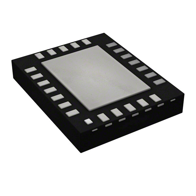
Device Information(1)
PART NUMBER
LP3943
PACKAGE
WQFN (24)
BODY SIZE (NOM)
4.00 mm × 4.00 mm
(1) For all available packages, see the orderable addendum at
the end of the data sheet.
Typical Application Circuit
+5V
R
5V
G
B
2
+5V
SMBUS/I C
Blue LEDs
VDD
LED15
SDA
SCL
PORTx.D
SDA
SCL
LED14
LED13
RESET
+5V
White LEDs
LED12
LED11
LED10
Cell Phone Baseband
Controller/PController
LED9
LED8
LED7
A2
A1
A0
LED6
LED5
LED4
LED3
LED2
GND
LED1
LED0
1
An IMPORTANT NOTICE at the end of this data sheet addresses availability, warranty, changes, use in safety-critical applications,
intellectual property matters and other important disclaimers. PRODUCTION DATA.
�LP3943
SNVS256D – NOVMEBER 2003 – REVISED NOVEMBER 2016
www.ti.com
Table of Contents
1
2
3
4
5
6
Features ..................................................................
Applications ...........................................................
Description .............................................................
Revision History.....................................................
Pin Configuration and Functions .........................
Specifications.........................................................
1
1
1
2
3
4
6.1
6.2
6.3
6.4
6.5
6.6
4
4
4
4
5
Absolute Maximum Ratings ......................................
ESD Ratings..............................................................
Recommended Operating Conditions.......................
Thermal Information ..................................................
Electrical Characteristics...........................................
I2C Interface (SCL and SDA Pins) Timing
Requirements.............................................................
6.7 Typical Characteristic ...............................................
7
6
6
Detailed Description .............................................. 7
7.1
7.2
7.3
7.4
Overview ...................................................................
Functional Block Diagram .........................................
Feature Description...................................................
Device Functional Modes..........................................
7
7
8
8
7.5 Programming............................................................. 9
7.6 Register Maps ......................................................... 12
8
Application and Implementation ........................ 15
8.1 Application Information............................................ 15
8.2 Typical Application ................................................. 15
8.3 System Examples ................................................... 17
9 Power Supply Recommendations...................... 17
10 Layout................................................................... 18
10.1 Layout Guidelines ................................................. 18
10.2 Layout Example .................................................... 18
11 Device and Documentation Support ................. 19
11.1
11.2
11.3
11.4
11.5
Receiving Notification of Documentation Updates
Community Resources..........................................
Trademarks ...........................................................
Electrostatic Discharge Caution ............................
Glossary ................................................................
19
19
19
19
19
12 Mechanical, Packaging, and Orderable
Information ........................................................... 19
4 Revision History
NOTE: Page numbers for previous revisions may differ from page numbers in the current version.
Changes from Revision C (October 2015) to Revision D
Page
•
Changed change wording of title to add SEO keywords ....................................................................................................... 1
•
Changed RθJA value from "37°C/W" to "45.0°C/W"; add additional thermal values ............................................................... 4
Changes from Revision B (September 2013) to Revision C
•
Added Device Information and Pin Configuration and Functions sections, ESD Ratings table, Feature Description,
Device Functional Modes, Application and Implementation, Power Supply Recommendations, Layout, Device and
Documentation Support, and Mechanical, Packaging, and Orderable Information sections. ............................................... 1
Changes from Revision A (April 2013) to Revision B
•
2
Page
Page
Changed layout of National Data Sheet to TI format; fixed format of Block Diagram............................................................ 7
Submit Documentation Feedback
Copyright © 2003–2016, Texas Instruments Incorporated
Product Folder Links: LP3943
�LP3943
www.ti.com
SNVS256D – NOVMEBER 2003 – REVISED NOVEMBER 2016
5 Pin Configuration and Functions
RTW Package
24-Pin WQFN With Exposed Pad
Top View
18
17
16
15
14
13
19
12
20
11
21
10
22
9
23
8
24
7
1
2
3
4
5
6
Pin Functions
PIN
I/O
DESCRIPTION
NUMBER
NAME
1
LED0
Output
Output of LED0 Driver
2
LED1
Output
Output of LED1 Driver
3
LED2
Output
Output of LED2 Driver
4
LED3
Output
Output of LED3 Driver
5
LED4
Output
Output of LED4 Driver
6
LED5
Output
Output of LED5 Driver
7
LED6
Output
Output of LED6 Driver
8
LED7
Output
Output of LED7 Driver
9
GND
Ground
Ground
10
LED8
Output
Output of LED8 Driver
11
LED9
Output
Output of LED9 Driver
12
LED10
Output
Output of LED10 Driver
13
LED11
Output
Output of LED11 Driver
14
LED12
Output
Output of LED12 Driver
15
LED13
Output
Output of LED13 Driver
16
LED14
Output
Output of LED14 Driver
17
LED15
Output
Output of LED15 Driver
18
RST
Input
Active Low Reset Input
19
SCL
Input
Clock Line for I2C Interface
20
SDA
Input/Output
21
VDD
Power
22
A0
Input
Address Input 0
23
A1
Input
Address Input 1
24
A2
Input
Address Input 2
—
Exposed Pad
—
Serial Data Line for I2C Interface
Power Supply
Tie internally to GND pin.
Submit Documentation Feedback
Copyright © 2003–2016, Texas Instruments Incorporated
Product Folder Links: LP3943
3
�LP3943
SNVS256D – NOVMEBER 2003 – REVISED NOVEMBER 2016
www.ti.com
6 Specifications
6.1 Absolute Maximum Ratings
over operating free-air temperature range (unless otherwise noted) (1) (2) (3)
VDD
MIN
MAX
UNIT
–0.5
6
V
6
V
6
V
A0, A1, A2, SCL, SDA, RST
(Collectively called digital pins)
VSS − 0.5
Voltage on LED pins
Junction temperature
150
°C
Power dissipation (4)
400
mW
150
°C
Storage temperature
(1)
(2)
(3)
(4)
–65
Stresses beyond those listed under Absolute Maximum Ratings may cause permanent damage to the device. These are stress ratings
only, which do not imply functional operation of the device at these or any other conditions beyond those indicated under Recommended
Operating Conditions. Exposure to absolute-maximum-rated conditions for extended periods may affect device reliability.
All voltages are with respect to the potential at the GND pin.
If Military/Aerospace specified devices are required, contact the Texas Instruments Sales Office/ Distributors for availability and
specifications.
The part cannot dissipate more than 400 mW.
6.2 ESD Ratings
VALUE
Electrostatic
discharge
V(ESD)
(1)
(2)
Human-body model (HBM), per ANSI/ESDA/JEDEC JS-001 (1)
±2000
Charged-device model (CDM), per JEDEC specification JESD22-C101 (2)
±1000
Machine model
±200
UNIT
V
JEDEC document JEP155 states that 500-V HBM allows safe manufacturing with a standard ESD control process.
JEDEC document JEP157 states that 250-V CDM allows safe manufacturing with a standard ESD control process.
6.3 Recommended Operating Conditions
over operating free-air temperature range (unless otherwise noted) (1) (2)
MIN
NOM
MAX
UNIT
VDD
2.3
5.5
V
Junction temperature
–40
125
°C
Operating ambient temperature
–40
85
°C
(1)
(2)
Absolute Maximum Ratings are limits beyond which damage to the device might occur. Recommended Operating Conditions are
conditions under which operation of the device is ensured. Recommended Operating Conditions do not imply ensured performance
limits. For verified performance limits and associated test conditions, see Electrical Characteristics.
All voltages are with respect to the potential at the GND pin.
6.4 Thermal Information
LP3943
THERMAL METRIC (1)
RTW (WQFN)
UNIT
24 PINS
RθJA
Junction-to-ambient thermal resistance
45.0
°C/W
RθJC(top)
Junction-to-case (top) thermal resistance
41.5
°C/W
RθJB
Junction-to-board thermal resistance
22.4
°C/W
ψJT
Junction-to-top characterization parameter
0.5
°C/W
ψJB
Junction-to-board characterization parameter
22.5
°C/W
RθJC(bot)
Junction-to-case (bottom) thermal resistance
3.7
°C/W
(1)
4
For more information about traditional and new thermal metrics, see the Semiconductor and IC Package Thermal Metrics application
report.
Submit Documentation Feedback
Copyright © 2003–2016, Texas Instruments Incorporated
Product Folder Links: LP3943
�LP3943
www.ti.com
SNVS256D – NOVMEBER 2003 – REVISED NOVEMBER 2016
6.5 Electrical Characteristics
Unless otherwise noted, VDD = 5.5 V. Typical values and limits apply for TJ = 25°C. Minimum and maximum limits apply over
the entire junction temperature range for operation, TJ = −40°C to +125°C. (1)
PARAMETER
TEST CONDITIONS
MIN
TYP
MAX
UNIT
POWER SUPPLY
VDD
Supply voltage
IQ
Supply current
5
5.5
No load
2.3
350
550
Standby
2
5
ΔIQ
Additional standby current
VDD = 5.5 V, every LED pin at
4.3 V
VPOR
Power-On Reset voltage
1.8
tw
Reset pulse width
10
2
1.96
V
µA
mA
V
ns
LED
VIL
Low level input voltage
−0.5
0.8
V
VIH
High level input voltage
2
5.5
V
VOL = 0.4 V, VDD = 2.3 V
Low level output current (2)
IOL
ILEAK
CI/O
Input leakage current
Input/output capacitance
9
VOL = 0.4 V, VDD = 3 V
12
VOL = 0.4 V, VDD = 5 V
15
VOL = 0.7 V, VDD = 2.3 V
15
VOL = 0.7 V, VDD = 3 V
20
VOL = 0.7 V, VDD = 5 V
25
VDD = 3.6 V, VIN = 0 V or VDD
−1
See
mA
1
µA
5
pF
−0.5
0.8
V
2
5.5
V
−1
1
µA
5
pF
(3)
2.6
ALL DIGITAL PINS (EXCEPT SCL AND SDA PINS)
VIL
LOW level input voltage
VIH
HIGH level input voltage
ILEAK
Input leakage current
CIN
Input capacitance
VIN = 0 V (3)
2.3
I2C INTERFACE (SCL AND SDA PINS)
VIL
LOW level input voltage
–0.5
0.3VDD
V
VIH
HIGH level input voltage
0.7VDD
5.5
V
VOL
LOW level output voltage
0
0.2VDD
V
IOL
LOW level output current
ƒCLK
Clock frequency
(1)
(2)
(3)
VOL = 0.4 V
3
6.5
mA
400
kHz
Limits are ensured. All electrical characteristics having room-temperature limits are tested during production with TJ = 25°C. All hot and
cold limits are ensured by correlating the electrical characteristics to process and temperature variations and applying statistical process
control.
Each LED pin must not exceed 25 mA and each octal (LED0–LED7; LED8–LED15) must not exceed 100 mA. The package must not
exceed a total of 200 mA.
Verified by design.
Submit Documentation Feedback
Copyright © 2003–2016, Texas Instruments Incorporated
Product Folder Links: LP3943
5
�LP3943
SNVS256D – NOVMEBER 2003 – REVISED NOVEMBER 2016
www.ti.com
6.6 I2C Interface (SCL and SDA Pins) Timing Requirements
See (1)
MIN
NOM
MAX
UNIT
tHOLD
Hold time repeated START condition
0.6
µs
tCLK-LP
CLK low period
1.3
µs
tCLK-HP
CLK high period
0.6
µs
tSU
Setup time repeated START condition
0.6
µs
tDATA-HOLD
Data hold time
300
ns
tDATA-SU
Data setup time
100
ns
tSU
Setup time for STOP condition
0.6
µs
tTRANS
Maximum pulse width of spikes that must be suppressed by the input filter
of both DATA and CLK signals
(1)
50
ns
All values verified by design.
6.7 Typical Characteristic
PERCENT VARIATION (%)
10
5
0
-5
-10
-40
-20
0
20
40
60
80
TEMPERATURE (°C)
TA = −40°C to +85°C
VDD = 2.3 V to 3 V
Figure 1. Frequency vs. Temperature
6
Submit Documentation Feedback
Copyright © 2003–2016, Texas Instruments Incorporated
Product Folder Links: LP3943
�LP3943
www.ti.com
SNVS256D – NOVMEBER 2003 – REVISED NOVEMBER 2016
7 Detailed Description
7.1 Overview
The LP3943 takes incoming data from the baseband controller and feeds them into several registers that control
the frequency and the duty cycle of the LEDs. Two prescaler registers and two PWM registers provide two
individual rates to dim or blink the LEDs (for more information on these registers, refer to Table 1). Each LED
can be programmed in one of four states: ON, OFF, DIM0 rate, or DIM1 rate. Two read-only registers provide
status on all 16 LEDs. The LP3943 can be used to drive RGB LEDs and/or single-color LEDs to create a colorful,
entertaining, and informative setting. Alternatively, it can also drive RGB LED as a flashlight. This is particularly
suitable for accessory functions in cellular phones and toys. Any LED pins not used to drive LED can be used for
general purpose parallel input/output (GPIO) expansion.
The LP3943 is equipped with power-on reset that holds the chip in a reset state until VDD reaches VPOR during
power up. Once VPOR is achieved, the LP3943 comes out of reset and initializes itself to the default state.
To bring the LP3943 into reset, hold the RST pin LOW for a period of TW. This puts the chip into its default state.
The LP3943 can only be programmed after RST signal is HIGH again.
7.2 Functional Block Diagram
A2 A1 A0
Input Register
SCL
I2C
Filters
SDA
I2C Bus
Control
Bit0 of Input Reg 1
LED Select Register
Bit1
Bit0 of
Select
Register
LS0
0
1
LED0
VDD
RST
Power-On Reset
Oscillator
Prescaler 0
Register
PWM 0
Register
Prescaler 1
Register
PWM 1
Register
COPIES
Bit 7 of Input Register2
Bit 6 of Select Register LS3
Bit 7 of Select Register LS3
0
1
LED15
PWM0 Register
PWM1 Register
Submit Documentation Feedback
Copyright © 2003–2016, Texas Instruments Incorporated
Product Folder Links: LP3943
7
�LP3943
SNVS256D – NOVMEBER 2003 – REVISED NOVEMBER 2016
www.ti.com
7.3 Feature Description
Some of the features of the LP3943 device are:
1. 16 low-side switches to control the current in 16 strings of LEDs with a maximum of 25 mA per switch or a
maximum of 200 mA total.
2. Programmable internal PWM dimming:
(a) Duty cycle control (8 bits). Any of the 16 current switches can be mapped to either PWM0 register or
PWM1 register. Each register offers 8-bit PWM duty cycle control.
(b) PWM Frequency control (8 bits). Any of the 16 current switches can be mapped to either PSC0 register
or PSC1 register. Each register offers 8-bit PWM frequency control from 0.625 Hz to 160 Hz.
3. RESET input.
4. Auto increment for I2C writes to reduce number of I2C clock pulses .
5. The LP3943 provides for an externally selectable I2C slave address via the ADR0, ADR1, and ADR2 inputs.
See Figure 4.
7.4 Device Functional Modes
1. Output set to high impedance. This is set by programming bits [B0 and B1] to 00 in the LS0, LS1, LS2, or
LS3 registers (see Table 2)
2. Output set to ON state (current switch pulls low). This turns the LED on at the full current in the specified
current switch bits [B0 and B1] set to 01 in the LS0, LS1, LS2, or LS3 registers (see Table 12).
3. Output set to toggle at the programmed PWM duty cycle and PWM frequency. This turns on or off the
specified current switch at the programmed PWM frequency and duty cycle. Each current switch is mapped
to either of the PWM0/PSC0 or PWM1/PSC1 pairs by setting [B0 and B1] to 10 or 11 in the LS0, LS1, LS2,
or LS3 registers (see Table 12).
8
Submit Documentation Feedback
Copyright © 2003–2016, Texas Instruments Incorporated
Product Folder Links: LP3943
�LP3943
www.ti.com
SNVS256D – NOVMEBER 2003 – REVISED NOVEMBER 2016
7.5 Programming
7.5.1 I2C Data Validity
The data on SDA line must be stable during the HIGH period of the clock signal (SCL). In other words, state of
the data line can only be changed when CLK is LOW.
Figure 2. I2C Data Validity
7.5.2 I2C START and STOP Conditions
START and STOP bits classify the beginning and the end of the I2C session. START condition is defined as SDA
signal transitioning from HIGH to LOW while SCL line is HIGH. STOP condition is defined as the SDA
transitioning from LOW to HIGH while SCL is HIGH. The I2C master always generates START and STOP bits.
The I2C bus is considered to be busy after START condition and free after STOP condition. During data
transmission, I2C master can generate repeated START conditions. First START and repeated START
conditions are equivalent, function-wise.
Figure 3. I2C START and STOP Conditions
7.5.3 Transferring Data
Every byte put on the SDA line must be eight bits long with the most significant bit (MSB) being transferred first.
The number of bytes that can be transmitted per transfer is unrestricted. Each byte of data has to be followed by
an acknowledge bit. The acknowledge related clock pulse is generated by the master. The transmitter releases
the SDA line (HIGH) during the acknowledge clock pulse. The receiver must pull down the SDA line during the
9th clock pulse, signifying an acknowledge. A receiver which has been addressed must generate an
acknowledge after each byte has been received.
After the START condition, a chip address is sent by the I2C master. This address is seven bits long followed by
an eighth bit which is a data direction bit (R/W). The LP3943 hardwires bits 7 to 4 and leaves bits 3 to 1
selectable, as shown in Figure 4. For the eighth bit, a “0” indicates a WRITE and a “1” indicates a READ. The
LP3943 supports only a WRITE during chip addressing. The second byte selects the register to which the data is
written. The third byte contains data to write to the selected register.
Figure 4. Chip Address Byte
Submit Documentation Feedback
Copyright © 2003–2016, Texas Instruments Incorporated
Product Folder Links: LP3943
9
�LP3943
SNVS256D – NOVMEBER 2003 – REVISED NOVEMBER 2016
www.ti.com
Programming (continued)
ack from slave
start
msb Chip Address lsb
w ack
id = h'xx
w ack
ack from slave
msb Register Add lsb
ack from slave
ack
msb
DATA
lsb
ack
address h'02 data
ack
stop
SCL
SDA
start
addr = h'02
ack
stop
w = write (SDA = “0”)
r = read (SDA = “1”)
ack = acknowledge (SDA pulled LOW by either master or slave)
rs = repeated start
xx = 60 to 67
Figure 5. LP3943 Register Write
However, if a READ function is to be accomplished, a WRITE function must precede the READ function, as
shown in Figure 6.
ack from slave
start
msb Chip Address lsb
w ack
ack from slave
msb Register Add lsb
repeated start
ack
rs
ack
rs
ack from slave
msb Chip Address lsb
r
ack
data from slave
msb
DATA
lsb
ack from master
ack stop
SCL
SDA
start
id = h'xx
w ack
addr = h'00
id = h'xx
r ack
address h'00 data
ack
stop
w = write (SDA = “0”)
r = read (SDA = “1”)
ack = acknowledge (SDA pulled LOW by either master or slave)
rs = repeated start
xx = 60 to 67
Figure 6. LP3943 Register Read
7.5.4 Auto Increment
Auto increment is a special feature supported by the LP3943 to eliminate repeated chip and register addressing
when data are to be written to or read from registers in sequential order. The auto increment bit is inside the
register address byte, as shown in Figure 7. Auto increment is enabled when this bit is programmed to “1” and
disabled when it is programmed to “0”.
Bits 5, 6 and 7 in the register address byte must always be zero.
Figure 7. Register Address Byte
10
Submit Documentation Feedback
Copyright © 2003–2016, Texas Instruments Incorporated
Product Folder Links: LP3943
�LP3943
www.ti.com
SNVS256D – NOVMEBER 2003 – REVISED NOVEMBER 2016
Programming (continued)
In the READ mode, when auto increment is enabled, I2C master could receive any number of bytes from LP3943
without selecting chip address and register address again. Every time the I2C master reads a register, the
LP3943 increments the register address, and the next data register is read. When I2C master reaches the last
register (09H), the register address rolls over to 00H.
In the WRITE mode, when auto increment is enabled, the LP3943 increments the register address every time I2C
master writes to register. When the last register (09H register) is reached, the register address rolls over to 02H,
not 00H, because the first two registers in LP3943 are read-only registers. It is possible to write to the first two
registers independently, and the LP3943 device will acknowledge, but the data is ignored.
If auto increment is disabled, and the I2C master does not change register address, it continues to write data into
the same register.
Figure 8. Programming With Auto Increment Disabled (in WRITE Mode)
Figure 9. Programming With Auto Increment Enabled (in WRITE Mode)
Submit Documentation Feedback
Copyright © 2003–2016, Texas Instruments Incorporated
Product Folder Links: LP3943
11
�LP3943
SNVS256D – NOVMEBER 2003 – REVISED NOVEMBER 2016
www.ti.com
7.6 Register Maps
Table 1. LP3943 Register Table
Address (Hex)
Register Name
Read/Write
Register Function
0x00
Input 1
Read Only
LED0–7 Input Register
0x01
Input 2
Read Only
LED8–15 Input Register
0x02
PSC0
R/W
Frequency Prescaler 0
0x03
PWM0
R/W
PWM Register 0
0x04
PSC1
R/W
Frequency Prescaler 1
0x05
PWM1
R/W
PWM Register 1
0x06
LS0
R/W
LED0–3 Selector
0x07
LS1
R/W
LED4–7 Selector
0x08
LS2
R/W
LED8–11 Selector
0x09
LS3
R/W
LED12–15 Selector
7.6.1 Binary Format for Input Registers (Read-only)—Address 0x00 and 0x01
Table 2. Address 0x00
Bit #
Default value
7
6
5
4
3
2
1
0
X
X
X
X
X
X
X
X
LED7
LED6
LED5
LED4
LED3
LED2
LED1
LED0
2
1
0
Table 3. Address 0x01
Bit #
Default value
7
6
5
4
3
X
X
X
X
X
X
X
X
LED15
LED14
LED13
LED12
LED11
LED10
LED9
LED8
7.6.2 Binary Format for Frequency Prescaler and PWM Registers — Address 0x02 to 0x05
Table 4. Address 0x02 (PSC0)
Bit #
7
6
5
4
3
2
1
0
Default value
0
0
0
0
0
0
0
0
Table 5. Address 0x03 (PWM0)
Bit #
7
6
5
4
3
2
1
0
Default value
1
0
0
0
0
0
0
0
Table 6. Address 0x04 (PSC1)
Bit #
7
6
5
4
3
2
1
0
Default value
0
0
0
0
0
0
0
0
Table 7. Address 0x05 (PWM1)
Bit #
7
6
5
4
3
2
1
0
Default value
1
0
0
0
0
0
0
0
12
Submit Documentation Feedback
Copyright © 2003–2016, Texas Instruments Incorporated
Product Folder Links: LP3943
�LP3943
www.ti.com
SNVS256D – NOVMEBER 2003 – REVISED NOVEMBER 2016
7.6.3 Binary Format for Selector Registers — Address 0x06 to 0x09
Table 8. Address 0x06 (LS0)
Bit #
Default value
7
6
5
4
3
2
1
0
0
0
0
0
0
0
0
0
B1
B0
B1
B0
B1
B0
B1
B0
LED3
LED2
LED1
LED0
Table 9. Address 0x07 (LS1)
Bit #
7
6
5
4
3
2
1
Default value
0
0
0
0
0
0
0
0
B1
B0
B1
B0
B1
B0
B1
B0
LED7
LED6
0
LED5
LED4
Table 10. Address 0x08 (LS2)
Bit #
7
6
5
4
3
2
1
Default value
0
0
0
0
0
0
0
0
B1
B0
B1
B0
B1
B0
B1
B0
LED11
LED10
0
LED9
LED8
Table 11. Address 0x09 (LS3)
Bit #
7
6
5
4
3
2
1
0
Default value
0
0
0
0
0
0
0
0
B0
B1
B0
B1
B0
B1
B1
LED15
LED14
LED13
B0
LED12
Table 12. LED States With Respect To Values in B1 and B0
B1
B0
0
0
Output Hi-Z
(LED off)
Function
0
1
Output LOW
(LED on)
1
0
Output dims
(DIM0 rate)
1
1
Output dims
(DIM1 rate)
Submit Documentation Feedback
Copyright © 2003–2016, Texas Instruments Incorporated
Product Folder Links: LP3943
13
�LP3943
SNVS256D – NOVMEBER 2003 – REVISED NOVEMBER 2016
www.ti.com
Programming Example:
• Dim LEDs 0 to 7 at 1 Hz at 25% duty cycle
• Dim LEDs 8 to 12 at 5 Hz at 50% duty cycle
• Set LEDs 13, 14 and 15 off
• Step 1: Set PSC0 to achieve DIM0 of 1 s
• Step 2: Set PWM0 duty cycle to 25%
• Step 3: Set PSC1 to achieve DIM1 of 0.2 s
• Step 4: Set PWM1 duty cycle to 50%
• Step 5: Set LEDs 13, 14 and 15 off by loading the data into LS3 register
• Step 6: Set LEDs 0 to 7 to point to DIM0
• Step 7: Set LEDs 8 to 12 to point to DIM1
Table 13. Programming Details
STEP
14
REGISTER NAME
SET TO (HEX)
1
Set DIM0 = 1 s
1 = (PSC0 + 1)/160
PSC0 = 159
DESCRIPTION
PSC0
0x09F
2
Set duty cycle to 25%
Duty Cycle = PWM0/256
PWM0 = 64
PWM0
0x40
3
Set DIM1 = 0.2s
0.2 = (PSC1 + 1)/160
PSC1 = 31
PSC1
0x1F
4
Set duty cycle to 50%
Duty Cycle = PWM1/256
PWM1 = 128
PWM1
0x80
5
LEDs 13, 14 and 15 off
Output = HIGH
LS3
0x03
6
LEDs 0 to 7
Output = DIM0
LS0, LS1
LS0 = 0xAA
LS1 = 0xAA
7
LEDs 8 to 12
Output = DIM1
LS2, LS3
LS2 = 0xFF
LS3 = 0x03
Submit Documentation Feedback
Copyright © 2003–2016, Texas Instruments Incorporated
Product Folder Links: LP3943
�LP3943
www.ti.com
SNVS256D – NOVMEBER 2003 – REVISED NOVEMBER 2016
8 Application and Implementation
NOTE
Information in the following applications sections is not part of the TI component
specification, and TI does not warrant its accuracy or completeness. TI’s customers are
responsible for determining suitability of components for their purposes. Customers should
validate and test their design implementation to confirm system functionality.
8.1 Application Information
The LP3943 is a 16-channel LED controller which has 16 low-side current switches. Each switch can control the
LED current in its respective LED or LEDs by modulating its duty cycle and frequency.
8.2 Typical Application
+5V
R
5V
G
B
2
+5V
SMBUS/I C
Blue LEDs
VDD
LED15
SDA
SDA
SCL
SCL
PORTx.D
LED14
+5V
LED13
White LEDs
RESET
LED12
LED11
LED10
Cell Phone Baseband
Controller/PController
LED9
LED8
LED7
A2
LED6
LED5
A1
LED4
A0
LED3
LED2
LED1
GND
LED0
Figure 10. LP3943 Typical Application
8.2.1 Design Requirements
For typical RGB LED light-driver applications, use the parameters listed in Table 14.
Table 14. Design Parameters
DESIGN PARAMETER
EXAMPLE VALUE
Minimum input voltage
2.3 V
Typical output voltage
5V
Output current
20 mA
Submit Documentation Feedback
Copyright © 2003–2016, Texas Instruments Incorporated
Product Folder Links: LP3943
15
�LP3943
SNVS256D – NOVMEBER 2003 – REVISED NOVEMBER 2016
www.ti.com
8.2.2 Detailed Design Procedure
8.2.2.1 Reducing IQ When LEDs are OFF
In many applications, the LEDs and the LP3943 share the same VDD, as shown in Figure 10. When the LEDs are
off, the LED pins are at a lower potential than VDD, causing extra supply current (ΔIQ). To minimize this current,
consider keeping the LED pins at a voltage equal to or greater than VDD.
Figure 11. Methods to Reduce IQ When LEDs are in OFF State
8.2.3 Application Curve
Driver Input Resistance (LEDX)
49
VLEDX = 0.4 V
VLEDX = 0.7 V
46
43
40
37
34
31
28
25
2.3
2.6
2.9
3.2
3.5
3.8
VIN (V)
4.1
4.4
4.7
5
D001
Figure 12. Typical LED Switch Resistance
16
Submit Documentation Feedback
Copyright © 2003–2016, Texas Instruments Incorporated
Product Folder Links: LP3943
�LP3943
www.ti.com
SNVS256D – NOVMEBER 2003 – REVISED NOVEMBER 2016
8.3 System Examples
VOUT
VDD
LM2750-5.0
2.2 PF
LED 15
VIN
2.7V to 5.5V
2.2 PF
CAP+
CFLY
1 PF
LP3943
CAPLED 0
Figure 13. LP3943 With 5-V Booster
5V
VDD
R
LP3943
G
B
LED 15
LED 14
LED 13
LED 12
LED 11
LED 10
LED 9
LED 8
LED 7
LED 6
LED 5
LED 4
LED 3
LED 2
LED 1
LED 0
5V
Figure 14. LP3943 Driving RGB LED as a Flash
9 Power Supply Recommendations
The LP3943 is designed to be powered from a 2.3-V minimum to a 5.5-V maximum supply input.
Submit Documentation Feedback
Copyright © 2003–2016, Texas Instruments Incorporated
Product Folder Links: LP3943
17
�LP3943
SNVS256D – NOVMEBER 2003 – REVISED NOVEMBER 2016
www.ti.com
10 Layout
10.1 Layout Guidelines
The LP3943 layout is not critical, but TI recommends providing a noise-free supply input at VDD. This typically
would require a 1-µF capacitor placed close to the VDD pin and ground.
10.2 Layout Example
/RST
LED15
LED14
LED13
LED12
LED11
SCL
LED10
SDA
LED9
VDD
LED8
A0
GND
A1
LED7
A2
LED6
1 µF
LED0
LED1
LED2
LED3
LED4
LED5
Figure 15. LP3943 Layout Example
18
Submit Documentation Feedback
Copyright © 2003–2016, Texas Instruments Incorporated
Product Folder Links: LP3943
�LP3943
www.ti.com
SNVS256D – NOVMEBER 2003 – REVISED NOVEMBER 2016
11 Device and Documentation Support
11.1 Receiving Notification of Documentation Updates
To receive notification of documentation updates, navigate to the device product folder on ti.com. In the upper
right corner, click on Alert me to register and receive a weekly digest of any product information that has
changed. For change details, review the revision history included in any revised document.
11.2 Community Resources
The following links connect to TI community resources. Linked contents are provided "AS IS" by the respective
contributors. They do not constitute TI specifications and do not necessarily reflect TI's views; see TI's Terms of
Use.
TI E2E™ Online Community TI's Engineer-to-Engineer (E2E) Community. Created to foster collaboration
among engineers. At e2e.ti.com, you can ask questions, share knowledge, explore ideas and help
solve problems with fellow engineers.
Design Support TI's Design Support Quickly find helpful E2E forums along with design support tools and
contact information for technical support.
11.3 Trademarks
E2E is a trademark of Texas Instruments.
All other trademarks are the property of their respective owners.
11.4 Electrostatic Discharge Caution
These devices have limited built-in ESD protection. The leads should be shorted together or the device placed in conductive foam
during storage or handling to prevent electrostatic damage to the MOS gates.
11.5 Glossary
SLYZ022 — TI Glossary.
This glossary lists and explains terms, acronyms, and definitions.
12 Mechanical, Packaging, and Orderable Information
The following pages include mechanical, packaging, and orderable information. This information is the most
current data available for the designated devices. This data is subject to change without notice and revision of
this document. For browser-based versions of this data sheet, refer to the left-hand navigation.
Submit Documentation Feedback
Copyright © 2003–2016, Texas Instruments Incorporated
Product Folder Links: LP3943
19
�PACKAGE OPTION ADDENDUM
www.ti.com
30-Sep-2021
PACKAGING INFORMATION
Orderable Device
Status
(1)
Package Type Package Pins Package
Drawing
Qty
Eco Plan
(2)
Lead finish/
Ball material
MSL Peak Temp
Op Temp (°C)
Device Marking
(3)
(4/5)
(6)
LP3943ISQ
ACTIVE
WQFN
RTW
24
1000
Non-RoHS
& Green
Call TI
Level-1-260C-UNLIM
-40 to 85
3943SQ
LP3943ISQ/NOPB
ACTIVE
WQFN
RTW
24
1000
RoHS & Green
SN
Level-1-260C-UNLIM
-40 to 85
3943SQ
LP3943ISQX/NOPB
ACTIVE
WQFN
RTW
24
4500
RoHS & Green
SN
Level-1-260C-UNLIM
-40 to 85
3943SQ
(1)
The marketing status values are defined as follows:
ACTIVE: Product device recommended for new designs.
LIFEBUY: TI has announced that the device will be discontinued, and a lifetime-buy period is in effect.
NRND: Not recommended for new designs. Device is in production to support existing customers, but TI does not recommend using this part in a new design.
PREVIEW: Device has been announced but is not in production. Samples may or may not be available.
OBSOLETE: TI has discontinued the production of the device.
(2)
RoHS: TI defines "RoHS" to mean semiconductor products that are compliant with the current EU RoHS requirements for all 10 RoHS substances, including the requirement that RoHS substance
do not exceed 0.1% by weight in homogeneous materials. Where designed to be soldered at high temperatures, "RoHS" products are suitable for use in specified lead-free processes. TI may
reference these types of products as "Pb-Free".
RoHS Exempt: TI defines "RoHS Exempt" to mean products that contain lead but are compliant with EU RoHS pursuant to a specific EU RoHS exemption.
Green: TI defines "Green" to mean the content of Chlorine (Cl) and Bromine (Br) based flame retardants meet JS709B low halogen requirements of