LP3986
www.ti.com
SNVS142U – AUGUST 2001 – REVISED FEBRUARY 2013
LP3986 Dual Micropower 150 mA Ultra Low-Dropout CMOS Voltage Regulators in DSBGA
Package
Check for Samples: LP3986
FEATURES
DESCRIPTION
•
•
The LP3986 is a 150 mA dual low dropout regulator
designed for portable and wireless applications with
demanding
performance
and
board
space
requirements.
1
2
•
•
•
•
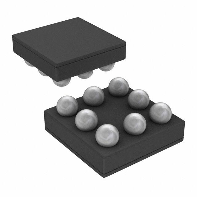
Miniature 8-I/O DSBGA Package
Stable With 1µF Ceramic and High Quality
Tantalum Output Capacitors
Fast Turn-on
Two Independent Regulators
Logic Controlled Enable
Over Current and Thermal Protection
APPLICATIONS
•
•
•
•
CDMA Cellular Handsets
GSM Cellular Handsets
Portable Information Appliances
Portable Battery Applications
The LP3986 is stable with a small 1 µF ±30%
ceramic output capacitor requiring smallest possible
board space.
The LP3986's performance is optimized for battery
powered systems to deliver ultra low noise, extremely
low dropout voltage and low quiescent current
independent of load current. Regulator ground current
increases very slightly in dropout, further prolonging
the battery life. Optional external bypass capacitor
reduces the output noise further without slowing down
the load transient response. Fast start-up time is
achieved by utilizing a speed-up circuit that actively
pre-charges the bypass capacitor. Power supply
rejection is better than 60 dB at low frequencies and
55 dB at 10 kHz. High power supply rejection is
maintained at low input voltage levels common to
battery operated circuits.
The LP3986 is available in a DSBGA package.
Performance is specified for a −40°C to +125°C
temperature range. For single LDO applications,
please refer to the LP3985 datasheet.
Table 1. Key Specifications
Guaranteed output current per regulator
VALUE
UNIT
150
mA
Typical quiescent current when both regulators in shutdown mode
1
nA
Typical dropout voltage at 150 mA output current
60
mV
Typical ground current
115
µA
Typical output noise
40
µV
Fast turn-on circuit
Junction temperature
200
µs
−40 to +125
°C
1
2
Please be aware that an important notice concerning availability, standard warranty, and use in critical applications of
Texas Instruments semiconductor products and disclaimers thereto appears at the end of this data sheet.
All trademarks are the property of their respective owners.
PRODUCTION DATA information is current as of publication date.
Products conform to specifications per the terms of the Texas
Instruments standard warranty. Production processing does not
necessarily include testing of all parameters.
Copyright © 2001–2013, Texas Instruments Incorporated
�LP3986
SNVS142U – AUGUST 2001 – REVISED FEBRUARY 2013
www.ti.com
Typical Application Circuit
Input
2.7V to 6.0V
VOUT1
VIN
CIN
LP3986
EN1
VOUT2
EN2
1PF
1PF
BYPASS
CBYPASS*
GND
0.01PF
Block Diagram
LP3986
VOUT2
VIN
VOUT1
BYPASS
Fast Turn
On
circuit
Vreference
1.23V
VEN2
VEN1
Over Current &
Thermal
Protection
GND
Pin Functions
PIN DESCRIPTIONS
(1)
2
Name
DSBGA (1)
VOUT2
A1
Output Voltage of the second LDO
EN2
B1
Enable input for the second LDO
BYPASS
C1
Bypass capacitor for the bandgap
GND
C2
Common ground
GND
C3
Common ground
EN1
B3
Enable input for the first LDO
VOUT1
A3
Output Voltage of the first LDO
VIN
A2
Common input for both LDOs
Function
The pin numbering scheme for the DSBGA package was revised in April 2002 to conform to JEDEC standard. Only the pin numbers
were revised. No changes to the physical location of the inputs/outputs were made. For reference purposes, the obsolete numbering
scheme had VOUT2 as pin 1, EN2 as pin 2, BYPASS as pin 3, GND as pins 4 and 5, EN1 as pin 6, VOUT1 as pin 7, and VIN as pin 8.
Submit Documentation Feedback
Copyright © 2001–2013, Texas Instruments Incorporated
Product Folder Links: LP3986
�LP3986
www.ti.com
SNVS142U – AUGUST 2001 – REVISED FEBRUARY 2013
Connection Diagram
8 Bump DSBGA Package – Top View
See Package Number YZR0008
These devices have limited built-in ESD protection. The leads should be shorted together or the device placed in conductive foam
during storage or handling to prevent electrostatic damage to the MOS gates.
Absolute Maximum Ratings
(1) (2) (3)
−0.3 to 6.5V
VIN, VEN
−0.3 to (VIN+0.3V) ≤ 6.5V
VOUT
Junction Temperature
150°C
Storage Temperature
−65°C to +150°C
Pad Temp.
(4)
Maximum Power Dissipation
235°C
(5)
364mW
ESD Rating (6)
Human Body Model
Machine Model
(1)
(2)
(3)
(4)
(5)
(6)
2kV
200V
Absolute Maximum Ratings are limits beyond which damage to the device may occur. Operating Ratings are conditions under which
operation of the device is guaranteed. Operating Ratings do not imply guaranteed performance limits. For guaranteed performance limits
and associated test conditions, see Electrical Characteristics.
All voltages are with respect to the potential at the GND pin.
If Military/Aerospace specified devices are required, please contact the Texas Instruments Sales Office / Distributors for
availability and specifications.
Additional information on pad temperature can be found in TI's AN-1112 application report (SNVA009).
The Absolute Maximum power dissipation depends on the ambient temperature and can be calculated using the formula: PD = (TJ TA)/θJA,Where TJ is the junction temperature, TA is the ambient temperature, and θJA is the junction-to-ambient thermal resistance. The
364mW rating appearing under Absolute Maximum Ratings results from substituting the Absolute Maximum junction temperature,
150°C, for TJ, 70°C for TA, and 220°C/W for θJA. More power can be dissipated safely at ambient temperatures below 70°C . Less
power can be dissipated safely at ambient temperatures above 70°C. The Absolute Maximum power dissipation can be increased by
4.5mW for each degree below 70°C, and it must be derated by 4.5mW for each degree above 70°C.
The human body model is 100pF discharged through a 1.5kΩ resistor into each pin. The machine model is a 200pF capacitor
discharged directly into each pin.
Submit Documentation Feedback
Copyright © 2001–2013, Texas Instruments Incorporated
Product Folder Links: LP3986
3
�LP3986
SNVS142U – AUGUST 2001 – REVISED FEBRUARY 2013
Operating Ratings
www.ti.com
(1) (2)
VIN
2.7 to 6V
VEN
0 to (VIN+ 0.3V) ≤ 6V
−40°C to +125°C
Junction Temperature
Thermal Resistance
θJA
220°C/W
Maximum Power Dissipation
(1)
(2)
(3)
(3)
250mW
Absolute Maximum Ratings are limits beyond which damage to the device may occur. Operating Ratings are conditions under which
operation of the device is guaranteed. Operating Ratings do not imply guaranteed performance limits. For guaranteed performance limits
and associated test conditions, see Electrical Characteristics.
All voltages are with respect to the potential at the GND pin.
Like the Absolute Maximum power dissipation, the maximum power dissipation for operation depends on the ambient temperature. The
250mW rating appearing under Operating Ratings results from substituting the maximum junction temperature for operation, 125°C, for
TJ, 70°C for TA, and 220°C/W for θJA into (1) above. More power can be dissipated at ambient temperatures below 70°C . Less power
can be dissipated at ambient temperatures above 70°C. The maximum power dissipation for operation can be increased by 4.5mW for
each degree below 70°C, and it must be derated by 4.5mW for each degree above 70°C.
Electrical Characteristics
Unless otherwise specified: VIN = VOUT(nom) + 0.5V, CIN = 1 µF, IOUT = 1mA, COUT = 1 µF, CBYPASS = 0.01µF. Typical values and
limits appearing in standard typeface are for TJ = 25°C. Limits appearing in boldface type apply over the entire junction
temperature range for operation, −40°C to +125°C. (1) (2)
Symbol
ΔVOUT
Parameter
Conditions
% of
VOUT(nom)
0.092
0.128
%/V
IOUT = 1mA to 150 mA
0.003
0.006
0.01
%/mA
(4)
Quiescent Current
VIN = VOUT(nom) + 1V,
IOUT = 150 mA (Figure 1)
1.5
VIN = 3.1V,
f = 1 kHz,
IOUT = 50 mA (Figure 2)
60
VIN = 3.1V,
f = 10 kHz,
IOUT = 50 mA (Figure 2)
50
Both Regulators ON
VEN = 1.4V, IOUT = 0 mA
115
200
Both Regulators ON
VEN = 1.4V, IOUT = 0 to 150 mA
220
320
One Regulator ON
VEN = 1.4V IOUT = 0 mA
75
130
One Regulator ON
VEN = 1.4V IOUT = 0 to 150 mA
130
200
0.001
2
4
2
100
VEN = 0.4V, Both Regulators OFF
(shutdown)
4
2.5
3.0
0.006
IQ
(5)
−2.5
−3.0
VIN = (VOUT(nom) + 0.5V) to 6.0V,
IOUT = 1 mA
Power Supply Rejection Ratio
(4)
Max
Line Regulation Error (3)
PSRR
(2)
(3)
Units
Min
IOUT = 1mA
Output AC Line Regulation
(1)
Limit
Output Voltage
Tolerance
Load Regulation Error
ISC
Typ
Dropout Voltage (5)
IOUT = 1 mA
IOUT = 150 mA
0.4
60
Short Circuit Current Limit
Output Grounded
600
mVP-P
dB
µA
mV
mA
All limits are guaranteed. All electrical characteristics having room temperature limits are tested during production with TJ = 25°C or
correlated using Statistical Quality Control (SQC) methods. All hot and cold limits are guaranteed by correlating the electrical
characteristics to process and temperature variations and applying statistical process control.
The target output voltage, which is labeled VOUT(nom), is the desired voltage option.
The output voltage changes slightly with line voltage. An increase in the line voltage results in a slight increase in the output voltage and
vice versa.
The output voltage changes slightly with load current. An increase in the load current results in a slight decrease in the output voltage
and vice versa. Tested limit applies to Vout 's of 2.5V and greater.
Dropout voltage is the input-to-output voltage difference at which the output voltage is 100mV below its nominal value.
Submit Documentation Feedback
Copyright © 2001–2013, Texas Instruments Incorporated
Product Folder Links: LP3986
�LP3986
www.ti.com
SNVS142U – AUGUST 2001 – REVISED FEBRUARY 2013
Electrical Characteristics (continued)
Unless otherwise specified: VIN = VOUT(nom) + 0.5V, CIN = 1 µF, IOUT = 1mA, COUT = 1 µF, CBYPASS = 0.01µF. Typical values and
limits appearing in standard typeface are for TJ = 25°C. Limits appearing in boldface type apply over the entire junction
temperature range for operation, −40°C to +125°C. (1) (2)
Symbol
IOUT(PK)
Parameter
Peak Output Current (6)
(7)
Conditions
Typ
VOUT ≥ VOUT(nom) - 5%
500
Limit
Min
Max
Units
300
mA
TON
Turn-On Time
CBYPASS = 0.01 µF
200
µs
en
Output Noise Voltage
BW = 10 Hz to 100 kHz,
COUT = 1µF
40
µVrms
ρn(1/f)
Output Noise Density
f = 120 Hz,
COUT = 1µF
1
µV/√Hz
IEN
Maximum Input Current at EN
VEN = 0.4 and VIN = 6V
VIL
Maximum Low Level Input
Voltage at EN
VIN = 2.7 to 6V
VIH
Minimum High Level Input
Voltage at EN
VIN = 2.7 to 6V
Xtalk
Crosstalk Rejection
−60
−60
Input capacitance (8)
If VOUT = 1.8V,
VIN_MIN>= 2.9V
COUT
Capacitance (8)
All VOUT > = 2.5V,
If VOUT = 1.8V,
VIN_MIN>= 2.9V
(6)
(7)
(8)
(9)
See
(9)
V
1.4
ΔILoad2 = 150 mA at 1KHz rate
ΔILoad1 = 1 mA
ΔVOUT2/ΔVOUT1
CIN
nA
0.4
ΔILoad1 = 150 mA at 1KHz rate
ΔILoad2 = 1 mA
ΔVOUT2/ΔVOUT1
All VOUT > = 2.5V,
ESR
±10
V
dB
1
µF
4.7
µF
1
22
µF
2.2
22
µF
5
500
mΩ
IPEAK guaranteed for Vout 's of 2.5V and greater.
Turn-on time is that between the enable input just exceeding VIH and the output voltage just reaching 95% of its nominal value.
Range of capacitor values for which the device will remain stable. This electrical specification is guaranteed by design.
Range of capacitor ESR values for which the device will remain stable. This electrical specification is guaranteed by design.
Submit Documentation Feedback
Copyright © 2001–2013, Texas Instruments Incorporated
Product Folder Links: LP3986
5
�LP3986
SNVS142U – AUGUST 2001 – REVISED FEBRUARY 2013
www.ti.com
TEST SIGNALS
Figure 1. Line Regulation Input Test Signal
Figure 2. PSRR Input Test Signal
6
Submit Documentation Feedback
Copyright © 2001–2013, Texas Instruments Incorporated
Product Folder Links: LP3986
�LP3986
www.ti.com
SNVS142U – AUGUST 2001 – REVISED FEBRUARY 2013
TYPICAL PERFORMANCE CHARACTERISTICS
Unless otherwise specified, CIN= COUT 1µF Ceramic, C BP= 0.01µ F, VIN = VOUT + 0.5, TA= 25°C, both enable pins are tied to
VIN
Power Supply Rejection Ratio (CBP = 0.001µF)
Power Supply Rejection Ratio (CBP = 0.01µF)
Figure 3.
Figure 4.
Power Supply Rejection Ratio (CBP = 0.1µF)
Output Noise Spectral Density
Figure 5.
Figure 6.
Line Transient Response (CBP = 0.001µF)
Line Transient Response (CBP = 0.01µF)
Figure 7.
Figure 8.
Submit Documentation Feedback
Copyright © 2001–2013, Texas Instruments Incorporated
Product Folder Links: LP3986
7
�LP3986
SNVS142U – AUGUST 2001 – REVISED FEBRUARY 2013
www.ti.com
TYPICAL PERFORMANCE CHARACTERISTICS (continued)
Unless otherwise specified, CIN= COUT 1µF Ceramic, C BP= 0.01µ F, VIN = VOUT + 0.5, TA= 25°C, both enable pins are tied to
VIN
8
Load Transient & Cross Talk (VIN = VOUT + 0.2V)
Load Transient & Cross Talk (VIN = VOUT + 0.2V)
Figure 9.
Figure 10.
Start-Up Time (CBP = 0.001, 0.01, 0.1µF)
Enable Response ( VIN = 4.2V )
Figure 11.
Figure 12.
Enable Response (VIN = VOUT+ 0.2V)
Enable Response
Figure 13.
Figure 14.
Submit Documentation Feedback
Copyright © 2001–2013, Texas Instruments Incorporated
Product Folder Links: LP3986
�LP3986
www.ti.com
SNVS142U – AUGUST 2001 – REVISED FEBRUARY 2013
TYPICAL PERFORMANCE CHARACTERISTICS (continued)
Unless otherwise specified, CIN= COUT 1µF Ceramic, C BP= 0.01µ F, VIN = VOUT + 0.5, TA= 25°C, both enable pins are tied to
VIN
Output Short Circuit Current at VIN = 6V
Output Short Circuit Current at VIN = 3.3V
Figure 15.
Figure 16.
Submit Documentation Feedback
Copyright © 2001–2013, Texas Instruments Incorporated
Product Folder Links: LP3986
9
�LP3986
SNVS142U – AUGUST 2001 – REVISED FEBRUARY 2013
www.ti.com
APPLICATION HINTS
EXTERNAL CAPACITORS
Like any low-dropout regulator, the LP3986 requires external capacitors for regulator stability. The LP3986 is
specifically designed for portable applications requiring minimum board space and smallest components. These
capacitors must be correctly selected for good performance.
INPUT CAPACITOR
An input capacitance of ≊ 1µF is required between the LP3986 input pin and ground (the amount of the
capacitance may be increased without limit).
This capacitor must be located a distance of not more than 1cm from the input pin and returned to a clean
analog ground. Any good quality ceramic, tantalum, or film capacitor may be used at the input.
Important: Tantalum capacitors can suffer catastrophic failures due to surge current when connected to a lowimpedance source of power (like a battery or a very large capacitor). If a tantalum capacitor is used at the input,
it must be guaranteed by the manufacturer to have a surge current rating sufficient for the application.
There are no requirements for the ESR on the input capacitor, but tolerance and temperature coefficient must be
considered when selecting the capacitor to ensure the capacitance will be ≊ 1µF over the entire operating
temperature range.
OUTPUT CAPACITOR
The LP3986 is designed specifically to work with very small ceramic output capacitors, any ceramic capacitor
(temperature characteristics X7R, X5R, Z5U or Y5V) in 1 to 22 µF range with 5mΩ to 500mΩ ESR range is
suitable in the LP3986 application circuit.
It may also be possible to use tantalum or film capacitors at the output, but these are not as attractive for
reasons of size and cost (see next section Capacitor Characteristics).
The output capacitor must meet the requirement for minimum amount of capacitance and also have an ESR
(Equivalent Series Resistance) value which is within a stable range.
NO-LOAD STABILITY
The LP3986 will remain stable and in regulation with no-load (other than the internal voltage divider). This is
specially important in CMOS RAM keep-alive applications.
CAPACITOR CHARACTERISTICS
The LP3986 is designed to work with ceramic capacitors on the output to take advantage of the benefits they
offer: for capacitance values in the range of 1µF to 4.7µF range, ceramic capacitors are the smallest, least
expensive and have the lowest ESR values (which makes them best for eliminating high frequency noise). The
ESR of a typical 1µF ceramic capacitor is in the range of 20 mΩ to 40 mΩ, which easily meets the ESR
requirement for stability by the LP3986.
The ceramic capacitor's capacitance can vary with temperature. The capacitor type X7R, which operates over a
temperature range of -55°C to +125°C, will only vary the capacitance to within ±15%. Most large value ceramic
capacitors (≊ 2.2µF) are manufactured with Z5U or Y5V temperature characteristics. Their capacitance can drop
by more than 50% as the temperature goes from 25°C to 85°C. Therefore, X7R is recommended over Z5U and
Y5 in applications where the ambient temperature will change significantly above or below 25°C.
Tantalum capacitors are less desirable than ceramic for use as output capacitors because they are more
expensive when comparing equivalent capacitance and voltage ratings in the 1µF to 4.7µF range.
Another important consideration is that tantalum capacitors have higher ESR values than equivalent size
ceramics. This means that while it may be possible to find a tantalum capacitor with an ESR value within the
stable range, it would have to be larger in capacitance (which means bigger and more costly ) than a ceramic
capacitor with the same ESR value. It should also be noted that the ESR of a typical tantalum will increase about
2:1 as the temperature goes from 25°C down to −40°C, so some guard band must be allowed.
10
Submit Documentation Feedback
Copyright © 2001–2013, Texas Instruments Incorporated
Product Folder Links: LP3986
�LP3986
www.ti.com
SNVS142U – AUGUST 2001 – REVISED FEBRUARY 2013
NOISE BYPASS CAPACITOR
Connecting a 0.01µF capacitor between the CBYPASS pin and ground significantly reduces noise on the regulator
output. This cap is connected directly to a high impedance node in the band gap reference circuit. Any significant
loading on this node will cause a change on the regulated output voltage. For this reason, DC leakage current
through this pin must be kept as low as possible for best output voltage accuracy. The use of this 0.01µF bypass
capacitor is strongly recommended to prevent overshoot on the output during start up.
The types of capacitors best suited for the noise bypass capacitor are ceramic and film. High-quality ceramic
capacitors with either NPO or COG dielectric typically have very low leakage. Polypropolene and polycarbonate
film capacitors are available in small surface-mount packages and typically have extremely low leakage current.
Unlike many other LDOs, addition of a noise reduction capacitor does not effect the transient response of the
device.
ON/OFF INPUT OPERATION
The LP3986 is turned off by pulling the VEN pin low, and turned on by pulling it high. If this feature is not used,
the VEN pin should be tied to VIN to keep the regulator output on at all times. To assure proper operation, the
signal source used to drive the VEN input must be able to swing above and below the specified turn-on/off voltage
thresholds listed in the Electrical Characteristics section under VIL and VIH.
FAST ON-TIME
The LP3986 outputs are turned on after Vref voltage reaches its final value (1.23V nominal). To speed up this
process, the noise reduction capacitor at the bypass pin is charged with an internal 70µA current source. The
current source is turned off when the bandgap voltage reaches approximately 95% of its final value. The turn on
time is determined by the time constant of the bypass capccitor. The smaller the capacitor value, the shorter the
turn on time, but less noise gets reduced. As a result, turn on time and noise reduction need to be taken into
design consideration when choosing the value of the bypass capacitor.
DSBGA MOUNTING
The DSBGA package requires specific mounting techniques which are detailed in TI's AN-1112 application report
(SNVA009), in particular the section Surface Mount Assembly Considerations.
For best results during assembly, alignment ordinals on the PC board may be used to facilitate placement of the
DSBGA device.
DSBGA LIGHT SENSITIVITY
Exposing the DSBGA device to direct sunlight will cause misoperation of the device. Light sources such as
halogen lamps can effect electrical performance if brought near to the device.
The wavelengths which have most detrimental effect are reds and infra-reds, which means that the fluorescent
lighting used inside most buildings has very little effect on performance. A DSBGA test board was brought to
within 1cm of a fluorescent desk lamp and the effect on the regulated output voltage was negligible, showing a
deviation of less than 0.1% from nominal.
Submit Documentation Feedback
Copyright © 2001–2013, Texas Instruments Incorporated
Product Folder Links: LP3986
11
�LP3986
SNVS142U – AUGUST 2001 – REVISED FEBRUARY 2013
www.ti.com
REVISION HISTORY
Changes from Revision T (February 2013) to Revision U
•
12
Page
Changed layout of National Data Sheet to TI format .......................................................................................................... 11
Submit Documentation Feedback
Copyright © 2001–2013, Texas Instruments Incorporated
Product Folder Links: LP3986
�PACKAGE OPTION ADDENDUM
www.ti.com
10-Dec-2020
PACKAGING INFORMATION
Orderable Device
Status
(1)
Package Type Package Pins Package
Drawing
Qty
Eco Plan
(2)
Lead finish/
Ball material
MSL Peak Temp
Op Temp (°C)
Device Marking
(3)
(4/5)
(6)
LP3986TL-2518/NOPB
ACTIVE
DSBGA
YZR
8
250
RoHS & Green
SNAGCU
Level-1-260C-UNLIM
D
30
LP3986TL-2525/NOPB
ACTIVE
DSBGA
YZR
8
250
RoHS & Green
SNAGCU
Level-1-260C-UNLIM
D
27
LP3986TL-2828/NOPB
ACTIVE
DSBGA
YZR
8
250
RoHS & Green
SNAGCU
Level-1-260C-UNLIM
-40 to 125
D
10
LP3986TL-3030/NOPB
ACTIVE
DSBGA
YZR
8
250
RoHS & Green
SNAGCU
Level-1-260C-UNLIM
-40 to 125
D
12
LP3986TLX285285/NOPB
ACTIVE
DSBGA
YZR
8
3000
RoHS & Green
SNAGCU
Level-1-260C-UNLIM
D
11
(1)
The marketing status values are defined as follows:
ACTIVE: Product device recommended for new designs.
LIFEBUY: TI has announced that the device will be discontinued, and a lifetime-buy period is in effect.
NRND: Not recommended for new designs. Device is in production to support existing customers, but TI does not recommend using this part in a new design.
PREVIEW: Device has been announced but is not in production. Samples may or may not be available.
OBSOLETE: TI has discontinued the production of the device.
(2)
RoHS: TI defines "RoHS" to mean semiconductor products that are compliant with the current EU RoHS requirements for all 10 RoHS substances, including the requirement that RoHS substance
do not exceed 0.1% by weight in homogeneous materials. Where designed to be soldered at high temperatures, "RoHS" products are suitable for use in specified lead-free processes. TI may
reference these types of products as "Pb-Free".
RoHS Exempt: TI defines "RoHS Exempt" to mean products that contain lead but are compliant with EU RoHS pursuant to a specific EU RoHS exemption.
Green: TI defines "Green" to mean the content of Chlorine (Cl) and Bromine (Br) based flame retardants meet JS709B low halogen requirements of