LP5522
www.ti.com
SNVS488A – JUNE 2007 – REVISED MARCH 2013
Programmable LED Driver
Check for Samples: LP5522
FEATURES
DESCRIPTION
•
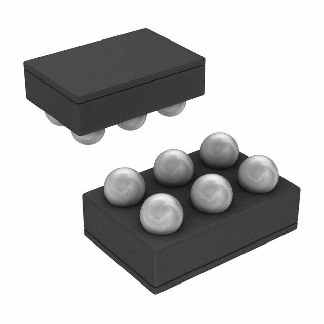
The LP5522 is a simple single wire programmable
LED controller in six bump DSBGA package. It
provides constant current flow through high side
driver. Output current can be set from 1 mA to 20 mA
by using an external resistor on the ISET pin. If no
external resistor is used, output current is set to 5 mA
default current. The LP5522 is controlled using only
one signal. The signal controls either directly the LED
driver or it launches previously programmed blinking
sequence.
1
2
•
•
•
•
•
Programmable Blinking Sequence
– 1 to 3 Programmable Pulses
– 1 ms to 255 ms LED on Time
– 10 ms to 2500 ms LED Off Time
– Single or Continuous Run of Programmed
Blinking Sequence
Constant Current High Side Output Driver
Adjustable Current with External Resistor
0.2 µA Typical Shutdown Current
Autonomous Operation without External Clock
DSBGA-6 Package with 0.4 mm Pitch:
– 1.215 mm x 0.815 mm x 0.6 mm (LxWxH)
The LP5522 works autonomously without a clock
signal from the master device. Very low LED driver
headroom voltage makes possible to use supply
voltages close to LED forward voltage. Current
consumption of the LP5522 is minimized when LED
is turned off and once controller is disabled all
supporting functions are also shut down. Very small
DSBGA package together with minimum number of
external components is a best fit for handheld
devices.
APPLICATIONS
•
•
•
Indicator Lights
Phone Cosmetics
Toys
Typical Application
VIN
VDD
ISET
+
-
LP5522
LED
CTRL
GND
GNDT
1
2
Please be aware that an important notice concerning availability, standard warranty, and use in critical applications of
Texas Instruments semiconductor products and disclaimers thereto appears at the end of this data sheet.
All trademarks are the property of their respective owners.
PRODUCTION DATA information is current as of publication date.
Products conform to specifications per the terms of the Texas
Instruments standard warranty. Production processing does not
necessarily include testing of all parameters.
Copyright © 2007–2013, Texas Instruments Incorporated
�LP5522
SNVS488A – JUNE 2007 – REVISED MARCH 2013
www.ti.com
Connection Diagrams
DSBGA-6 package, 0.815 x 1.215 x 0.60 mm body size, 0.4 mm pitch, Package Number YFQ0006
2
LED
GND
GNDT
GNDT
GND
LED
2
1
VDD
ISET
CTRL
CTRL
ISET
VDD
1
A
B
C
C
B
A
Figure 1. Top View
Figure 2. Bottom View
PIN DESCRIPTIONS (1)
(1)
Pin
Name
Type
A1
VDD
P
Power supply pin
Description
B1
ISET
AI
Current set input
C1
CTRL
DI
Digital control input
A2
LED
AO
Current source output
B2
GND
G
Ground
C2
GNDT
G
Ground
A: Analog Pin, D: Digital Pin, G: Ground Pin, P: Power Pin, I: Input Pin, O: Output Pin
These devices have limited built-in ESD protection. The leads should be shorted together or the device placed in conductive foam
during storage or handling to prevent electrostatic damage to the MOS gates.
Absolute Maximum Ratings
(1) (2) (3)
V (VDD, LED, ISET)
-0.3V to +6.0V
Voltage on logic pin (CTRL)
Continuous Power Dissipation
-0.3V to VDD +0.3V
with 6.0V max
(4)
Internally Limited
Junction Temperature (TJ-MAX)
125°C
Storage Temperature Range
-65°C to +150°C
Maximum Lead Temperature (Reflow soldering, 3 times)
(5)
ESD Rating (6)
Human Body Model
(1)
(2)
(3)
(4)
(5)
(6)
2
260°C
2 kV
Absolute Maximum Ratings indicate limits beyond which damage to the component may occur. Operating Ratings are conditions under
which operation of the device is ensured. Operating Ratings do not imply ensured performance limits. For ensured performance limits
and associated test conditions, see the Electrical Characteristics tables.
All voltages are with respect to the potential at the GND pins.
If Military/Aerospace specified devices are required, please contact the Texas Instruments Office/ Distributors for availability and
specifications.
Internal thermal shutdown circuitry protects the device from permanent damage. Thermal shutdown engages at TJ=160°C (typ.) and
disengages at TJ=140°C (typ.).
For detailed soldering specifications and information, please refer to Application Note AN1112 : DSBGA Wafer Level Chip Scale
Package SNVA009.
The Human body model is a 100 pF capacitor discharged through a 1.5 kΩ resistor into each pin. MIL-STD-883 3015.7
Submit Documentation Feedback
Copyright © 2007–2013, Texas Instruments Incorporated
Product Folder Links: LP5522
�LP5522
www.ti.com
Operating Ratings
SNVS488A – JUNE 2007 – REVISED MARCH 2013
(1) (2)
Voltage on power pin (VDD)
2.7V to 5.5V
Recommended Load Current
1 mA to 20 mA
Junction Temperature (TJ) Range
Ambient Temperature (TA) Range
(1)
(2)
(3)
-30°C to +125°C
(3)
-30°C to +85°C
Absolute Maximum Ratings indicate limits beyond which damage to the component may occur. Operating Ratings are conditions under
which operation of the device is ensured. Operating Ratings do not imply ensured performance limits. For ensured performance limits
and associated test conditions, see the Electrical Characteristics tables.
All voltages are with respect to the potential at the GND pins.
In applications where high power dissipation and/or poor package thermal resistance is present, the maximum ambient temperature may
have to be derated. Maximum ambient temperature (TA-MAX) is dependent on the maximum operating junction temperature (TJ-MAX-OP =
125°C), the maximum power dissipation of the device in the application (PD-MAX), and the junction-to ambient thermal resistance of the
part/package in the application (θJA), as given by the following equation: TA-MAX = TJ-MAX-OP – (θJA × PD-MAX).
Thermal Properties
Junction-to-Ambient Thermal Resistance (θJA) (1)
(1)
87°C/W
Junction-to-ambient thermal resistance is highly application and board-layout dependent. In applications where high maximum power
dissipation exists, special care must be paid to thermal dissipation issues in board design.
Submit Documentation Feedback
Copyright © 2007–2013, Texas Instruments Incorporated
Product Folder Links: LP5522
3
�LP5522
SNVS488A – JUNE 2007 – REVISED MARCH 2013
Electrical Characteristics
www.ti.com
(1) (2)
Limits in standard typeface are for TJ = 25°C. Limits in boldface type apply over the operating ambient temperature range (30°C < TA < +85°C). Unless otherwise noted, specifications apply to LP5522 Block Diagram with: VIN = 3.6V, RISET = 24 kΩ,
CIN = 100 nF.
Symbol
IVDD
Typ
Max
Units
Standby supply current
Parameter
CTRL = L
Condition
0.2
1
µA
Active Mode Supply Current
CTRL = H, LED = off
40
55
µA
5
ILEAKAGE
LED Pin Leakage Current
IOUT
LED Output Current
Without external resistor
LED Output Current
With external 24kΩ 0.04% resistor
Min
1
µA
+8
mA
%
+8
mA
%
35
50
mV
−8
20
−8
IMIRROR
External RISET
Mirroring Ratio
1:400
VISET
ISET Reference Voltage
VHR
Minimum Headroom Voltage
(VIN - VLED) (3)
70
100
mV
T_CYCLE_H
Minimum LED On Time
0.9
1.0
1.1
ms
T_CYCLE_L
Minimum LED Off Time
9
10
11
ms
ONRESOLUTION
LED On Time Resolution
1
ms
OFFRESOLUTIO
LED Off Time Resolution
10
ms
1.23
IOUT set to 10 mA
IOUT set to 20 mA
V
N
T_Timeout_H
LED Timeout On Time
287
319
351
ms
T_Timeout_L
LED Timeout Off Time
2.87
3.19
3.51
s
VIL
Logic Input Low Level
0.5
V
VIH
Logic Input High Level
1.2
IIN
CTRL Input Current
-1
1
µA
tON
CTRL Pulse ON Time
15
µs
tOFF
CTRL Pulse OFF Time
30
µs
tENTER
Command Entering Period
500
tENTER+tBLANK
Command Entering Period +
Blank Period
(1)
(2)
(3)
4
V
µs
1500
µs
All voltages are with respect to the potential at the GND pins.
Min and Max limits are ensured by design, test, or statistical analysis. Typical numbers are not ensured, but do represent the most likely
norm.
The current source is connected internally between VIN an VLED. The voltage across the current source, (VIN - VLED), is referred to a
headroom voltage (VHR). Minimum headroom voltage is defined as the VHR voltage when the LED current has dropped 10% from the
value measured at VLED = VIN - 1V.
Submit Documentation Feedback
Copyright © 2007–2013, Texas Instruments Incorporated
Product Folder Links: LP5522
�LP5522
www.ti.com
SNVS488A – JUNE 2007 – REVISED MARCH 2013
LP5522 BLOCK DIAGRAM
Submit Documentation Feedback
Copyright © 2007–2013, Texas Instruments Incorporated
Product Folder Links: LP5522
5
�LP5522
SNVS488A – JUNE 2007 – REVISED MARCH 2013
www.ti.com
Modes of Operation
POR
RESET
POR = H
POR = L
STANDBY
Control command
Control command
ends
ACTIVE
RESET In the reset mode all functions are off and all registers are reset to the default values. Reset is entered
always if internal Power On Reset (POR) is active. Power On Reset will activate during the device startup
or when the supply voltage VIN falls below 1.5V (typ.).
STANDBY: After Power On Reset device is in Standby mode. This is the low power consumption mode, when
all circuit functions are disabled.
ACTIVE: Once rising edge of CTRL signal is detected device goes into Active mode. In Active mode four sub
modes are present:
RUN: Run mode is divided into two sub modes depending on whether a blinking sequence is programmed into
memory or not.
Non-programmed mode: No blinking sequence programmed to memory. LED output follows CTRL input
Programmed mode: Blinking sequence programmed to memory. LED output follows the programmed blinking
sequence
RUN ONCE: In Run once mode, programmed blinking sequence is performed once and after that device
returns into Standby mode. Run once mode is available only if a blinking sequence is programmed into
memory.
TRAINING: In Training mode new blinking sequence can be programmed. LED output follows CTRL signal
during the programming
TSD: If chip temperature rises above 160°C (typ.) device goes into Thermal Shut Down (TSD) mode. In TSD
mode output is disabled but supporting functions are on.
LED Driver Operational Description
The LP5522 LED driver is constant current source. Current can be set with external resistor (RISET) so that the
current ratio between resistor and LED is 1:400. RISET current correlates to ISET reference voltage (VISET).
Consequently, current through LED can be adjusted using equation IOUT = 480/RISET.
Use of external resistor is optional. If external resistor is not connected, default output current is 5 mA. When
external resistor is not used ISET pin should be connected to VDD.
6
Submit Documentation Feedback
Copyright © 2007–2013, Texas Instruments Incorporated
Product Folder Links: LP5522
�LP5522
www.ti.com
SNVS488A – JUNE 2007 – REVISED MARCH 2013
LED Driver Typical Performance Characteristics
TJ = 25°C. Unless otherwise noted, typical performance characteristics apply to LP5522 Block Diagram with: VIN = 3.6V, RISET
= 24 kΩ, CIN = 100 nF.
Output Current vs RISET (Expanded Range)
Output Current vs RISET
Figure 3.
Figure 4.
Output Current vs Input Voltage
(ISET Connected To VDD)
Output Current vs Headroom Voltage
Figure 5.
Figure 6.
Line Regulation
LED Startup
Figure 7.
Figure 8.
Submit Documentation Feedback
Copyright © 2007–2013, Texas Instruments Incorporated
Product Folder Links: LP5522
7
�LP5522
SNVS488A – JUNE 2007 – REVISED MARCH 2013
www.ti.com
CONTROL INTERFACE OPERATIONAL DESCRIPTION
LP5522 has one digital control input, CTRL. Threshold levels of CTRL input are fixed to enable control from low
voltage controller. CTRL signal is used to control the mode of the circuit. A rising edge of the CTRL signal
activates the circuit and starts a command entering period. During the command entering period all rising edges
are counted. After command entering period there is a blank period when no rising edges are allowed. If CTRL is
left high after command entering period, the consequent command is performed right after the blank period.
Note that timing diagrams are not on scale!
CTRL
LED
Command entering period
Blank period
Command execution
starts
If CTRL signal is low after command entering period, command execution starts when CTRL is pulled high. This
does not apply to Run command. With Run command CTRL must be high. Note that no rising edges are allowed
during blank period.
CTRL
LED
Command entering period
Blank period
Command execution
starts
LED Controller Commands and Operation
There are four commands available for LP5522.
Command
Number of rising edges during command entering period
Run
One rising edge
Training start
Two rising edges
Training end
Three rising edges
Run once
Four rising edges
RUN COMMAND
One rising edge of CTRL signal within command entering period is interpreted as Run command. In programmed
mode blinking sequence is started right after Blank period and it is repeated as long as CTRL signal is kept high.
When CTRL signal is set low device goes into Standby mode.
8
Submit Documentation Feedback
Copyright © 2007–2013, Texas Instruments Incorporated
Product Folder Links: LP5522
�LP5522
www.ti.com
SNVS488A – JUNE 2007 – REVISED MARCH 2013
CTRL
To Standby
LED
Command entering
period
Blank period
Programmed sequence
In non-programmed mode LED is on as long as CTRL is kept high. When CTRL signal is set low device goes
into Standby mode.
CTRL
To Standby
LED
Command entering
period
Blank period
RUN ONCE COMMAND
Programmed blinking sequence is performed once after Run Once command. Four rising edges of CTRL signal
within command entering period is interpreted as Run Once command. If CTRL is kept high after command
entering period the programmed blinking sequence starts right after the blank period has elapsed. CTRL signal
must stay high as long as programmed blinking sequence is executed. If CTRL is set low during execution of
blinking sequence, device goes to standby and execution of blinking sequence is stopped.
CTRL
To Standby
Programmed sequence
LED
Command entering
period
Blank period
If CTRL signal is low after command entering period, Run Once command is executed once the CTRL is set
high.
CTRL
To Standby
Programmed sequence
LED
Command entering
period
Blank period
Submit Documentation Feedback
Copyright © 2007–2013, Texas Instruments Incorporated
Product Folder Links: LP5522
9
�LP5522
SNVS488A – JUNE 2007 – REVISED MARCH 2013
www.ti.com
TRAINING START COMMAND
Blinking sequence is programmed into memory in training mode. Blinking sequence is stored into volatile
memory, thus removing input voltage VIN resets the memory. Memory can also be reset by giving Training Start
and Training End commands without any valid LED ON/OFF times.
LP5522 enters to Training mode after Training Start command. Two rising edges within command entering
period is interpreted as the Training Start command. The first LED ON time capturing is started once the rising
edge of CTRL signal is detected after the blank period. LED output follows CTRL signal during the programming.
The first LED ON time is recorded once CTRL signal is set low. Same time the first LED OFF time capturing is
started. Programmed blinking sequence can have one to three LED ON/OFF times. In order to be programmed
correctly, at least one valid LED ON and LED OFF time must be recorded.
CTRL
LED
Command entering
period
Blank period
1st ON Time
1st OFF Time
starts
TRAINING END COMMAND
Blinking sequence programming ends once Training End command is introduced. Three rising edges within time
period of tENTER is interpreted as Training End command. Note that blank period is also reguired after Training
End command. During blanc period no rising edges are allowed.
When Training End command is introduced during LED OFF time capturing, LED OFF time is recorded and chip
goes to standby mode.
To Standby
CTRL
LED
1st ON time
1st OFF time
2nd ON
time
2nd OFF
time
tENTER
Blank period
If Training End command is introduced during LED ON time capturing, the associated LED ON period is not
recorded and hence neither OFF time. Notice that valid OFF time before Training End is longer than half of
Minimum LED OFF period (T_CYCLE_L).
10
Submit Documentation Feedback
Copyright © 2007–2013, Texas Instruments Incorporated
Product Folder Links: LP5522
�LP5522
www.ti.com
SNVS488A – JUNE 2007 – REVISED MARCH 2013
To Standby
CTRL
LED
1st ON time
1st OFF time
2nd ON
time
tENTER
Blank period
t < ½*T_CYCLE_L
LED TIMEOUT ON/OFF TIMES
When LP5522 is in training mode and CTRL signal is high longer than LED Timeout ON time, the ON time
counter saturates. In this case saturated ON time is recorded and LED OFF time capturing is started. At the
same time LED is switched off even if the CTRL signal is still high.
If ON time counter has saturated, LED OFF time recording is terminated either by giving a Train End command
or setting the CTRL signal to low and back to high. Setting the CTRL signal back to high records the LED OFF
time and starts next ON time capturing.
If anyhow CTRL is still high after the LED Timeout OFF time has been elapsed the OFF time counter saturates
and saturated OFF time is recorded. After that chip waits the CTRL signal to go low which cause the chip to go
Standby.
To Standby
Run command
CTRL
LED
tENTER + tBLANK
T_TIMEOUT_H T_TIMEOUT_L
LED OFF time counter can saturate also if Training end command is not given or no new ON time has been
started. In this case saturated OFF time is recorded and chip goes to Standby.
To Standby
Run once command
To Standby
CTRL
LED
tENTER + tBLANK
T_TIMEOUT_L
Submit Documentation Feedback
Copyright © 2007–2013, Texas Instruments Incorporated
Product Folder Links: LP5522
11
�LP5522
SNVS488A – JUNE 2007 – REVISED MARCH 2013
www.ti.com
Recommended External Components
INPUT CAPACITOR, CIN
Although not required for normal operation, a capacitor can be added to VIN to reduce line noise. A surfacemount multi-layer ceramic capacitor (MLCC) is recommended. MLCCs with a X7R or X5R temperature
characteristic are preferred.
CURRENT SET RESISTOR, RISET
If other than 5 mA current is required, RISET resistor can be used to adjust the current. For 20 mA current 24 kΩ
resistor is required. Accuracy of the resistor directly effects to the accuracy of the LED current. 1% or better is
recommended.
LED
Forward voltage of LED must be less than minimum input voltage minus minimum headroom voltage (VHR). For
example with 2.7V input voltage and 20 mA LED current the maximum LED forward voltage is 2.7V - 100 mV =
2.6V.
List of Recommended External Components
Symbol
Symbol Explanation
Value
Unit
Type
CIN
VDD Bypass Capacitor
100
nF
Ceramic, X7R or X5R
RISET
Current Set Resistor for 20 mA LED Current
24
kΩ
1%
LED
12
User defined
Submit Documentation Feedback
Copyright © 2007–2013, Texas Instruments Incorporated
Product Folder Links: LP5522
�LP5522
www.ti.com
SNVS488A – JUNE 2007 – REVISED MARCH 2013
REVISION HISTORY
Changes from Original (March 2013) to Revision A
•
Page
Changed layout of National Data Sheet to TI format .......................................................................................................... 12
Submit Documentation Feedback
Copyright © 2007–2013, Texas Instruments Incorporated
Product Folder Links: LP5522
13
�PACKAGE OPTION ADDENDUM
www.ti.com
10-Dec-2020
PACKAGING INFORMATION
Orderable Device
Status
(1)
Package Type Package Pins Package
Drawing
Qty
Eco Plan
(2)
Lead finish/
Ball material
MSL Peak Temp
Op Temp (°C)
Device Marking
(3)
(4/5)
(6)
LP5522TM/NOPB
ACTIVE
DSBGA
YFQ
6
250
RoHS & Green
SNAGCU
Level-1-260C-UNLIM
-30 to 85
6
LP5522TMX/NOPB
ACTIVE
DSBGA
YFQ
6
3000
RoHS & Green
SNAGCU
Level-1-260C-UNLIM
-30 to 85
6
(1)
The marketing status values are defined as follows:
ACTIVE: Product device recommended for new designs.
LIFEBUY: TI has announced that the device will be discontinued, and a lifetime-buy period is in effect.
NRND: Not recommended for new designs. Device is in production to support existing customers, but TI does not recommend using this part in a new design.
PREVIEW: Device has been announced but is not in production. Samples may or may not be available.
OBSOLETE: TI has discontinued the production of the device.
(2)
RoHS: TI defines "RoHS" to mean semiconductor products that are compliant with the current EU RoHS requirements for all 10 RoHS substances, including the requirement that RoHS substance
do not exceed 0.1% by weight in homogeneous materials. Where designed to be soldered at high temperatures, "RoHS" products are suitable for use in specified lead-free processes. TI may
reference these types of products as "Pb-Free".
RoHS Exempt: TI defines "RoHS Exempt" to mean products that contain lead but are compliant with EU RoHS pursuant to a specific EU RoHS exemption.
Green: TI defines "Green" to mean the content of Chlorine (Cl) and Bromine (Br) based flame retardants meet JS709B low halogen requirements of