Sample &
Buy
Product
Folder
Support &
Community
Tools &
Software
Technical
Documents
LP5524
SNVS500C – JULY 2007 – REVISED NOVEMBER 2016
LP5524 Four-Channel LED Driver With Dual-PWM Brightness Control
1 Features
3 Description
•
•
•
•
•
•
•
•
•
The LP5524 device is a highly integrated dual-zone
LED driver that can drive up to four LEDs in parallel
with a total output current of 100 mA. Regulated highside internal current sources deliver excellent current
and brightness matching in all LEDs.
1
Wide Input Voltage Range: 2.7 V to 5.5 V
High-Side LED Driver
Drives Four LEDs With up to 25 mA per LED
0.4% Typical Current Matching
PWM Brightness Control
Overcurrent Protection
Fast Transient Response
Optional External ISET Resistor
Ultra-Small Solution Size:
– No External Components
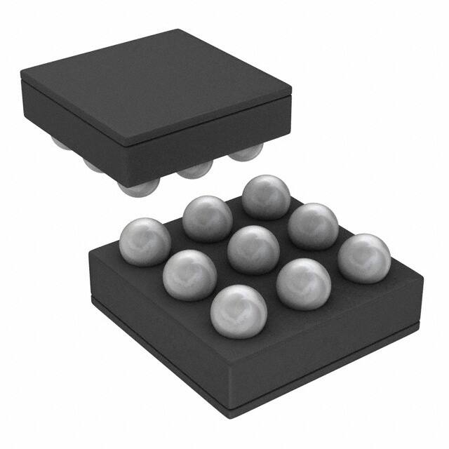
– 9-Pin DSBGA Package with 0.4-mm pitch:
– 1.24 mm × 1.24 mm × 0.6 mm (L × W × H,
maximum)
The LP5524 provides overcurrent protection and
pulse-width modulation (PWM) control of four
indicator LEDs without the need for external
components.
LED driver current sources are split into two
independently controlled banks for driving secondary
displays, keypad and indicator LEDs. Brightness
control is achieved by applying PWM signals to each
enable pin. Default LED current is factoryprogrammable and an optional external resistor can
be used to set LED current to user programmable
values.
2 Applications
•
•
•
The LP5524 is available in a tiny, 9-pin, thin DSBGA
package.
Sub-Display Backlight
Keypad LED Backlight
Indicator LED
Device Information(1)
PART NUMBER
LP5524
PACKAGE
DSBGA (9)
BODY SIZE (NOM)
1.21 mm × 1.21 mm
(1) For all available packages, see the orderable addendum at
the end of the data sheet.
space
space
space
space
Simplified Schematic
IDX = 25 mA max
VIN
VIN
D1A
ENA
D2A
LP5524
ENB
D1B
ISET
RISET
(optional)
D2B
GND
Copyright © 2016, Texas Instruments Incorporated
1
An IMPORTANT NOTICE at the end of this data sheet addresses availability, warranty, changes, use in safety-critical applications,
intellectual property matters and other important disclaimers. PRODUCTION DATA.
�LP5524
SNVS500C – JULY 2007 – REVISED NOVEMBER 2016
www.ti.com
Table of Contents
1
2
3
4
5
6
7
Features ..................................................................
Applications ...........................................................
Description .............................................................
Revision History.....................................................
Pin Configuration and Functions .........................
Specifications.........................................................
1
1
1
2
3
4
6.1
6.2
6.3
6.4
6.5
6.6
4
4
4
4
5
6
Absolute Maximum Ratings ......................................
ESD Ratings..............................................................
Recommended Operating Conditions.......................
Thermal Information ..................................................
Electrical Characteristics...........................................
LED Driver Typical Characteristics ...........................
Detailed Description .............................................. 7
7.1 Overview ................................................................... 7
7.2 Functional Block Diagram ......................................... 7
7.3 Feature Description................................................... 7
7.4 Device Functional Modes.......................................... 8
8
Application and Implementation .......................... 9
8.1 Application Information.............................................. 9
8.2 Typical Application ................................................... 9
9 Power Supply Recommendations...................... 11
10 Layout................................................................... 12
10.1 Layout Guidelines ................................................. 12
10.2 Layout Example .................................................... 12
11 Device and Documentation Support ................. 13
11.1
11.2
11.3
11.4
11.5
11.6
Documentation Support ........................................
Receiving Notification of Documentation Updates
Community Resources..........................................
Trademarks ...........................................................
Electrostatic Discharge Caution ............................
Glossary ................................................................
13
13
13
13
13
13
12 Mechanical, Packaging, and Orderable
Information ........................................................... 13
4 Revision History
NOTE: Page numbers for previous revisions may differ from page numbers in the current version.
Changes from Revision B (June 2016) to Revision C
•
Page
Changed wording of data sheet title ...................................................................................................................................... 1
Changes from Revision A (May 2013) to Revision B
Page
•
Added Device Information and Pin Configuration and Functions sections, ESD Ratings table, Feature Description,
Device Functional Modes, Application and Implementation, Power Supply Recommendations, Layout, Device and
Documentation Support, and Mechanical, Packaging, and Orderable Information sections ................................................. 1
•
Deleted lead temperature and soldering rows from Abs Max table - information in POA ..................................................... 4
•
Added Thermal Information table with revised RθJA value (from "80 - 125°C/W" to "101.9°C/W") and added
additional thermal values. ...................................................................................................................................................... 4
Changes from Original (April 2013) to Revision A
•
2
Page
Changed layout of National Data Sheet to TI format ........................................................................................................... 10
Submit Documentation Feedback
Copyright © 2007–2016, Texas Instruments Incorporated
Product Folder Links: LP5524
�LP5524
www.ti.com
SNVS500C – JULY 2007 – REVISED NOVEMBER 2016
5 Pin Configuration and Functions
YFQ Package
9-Pin DSBGA
Top View
YFQ Package
9-Pin DSBGA
Bottom View
3
ENA
D1A
D2A
D2A
D1A
ENA
3
2
ENB
VIN
GND
GND
VIN
ENB
2
1
ISET
D1B
D2B
D2B
D1B
ISET
1
A
B
C
C
B
A
Pin Functions
PIN
NUMBER
NAME
TYPE (1)
DESCRIPTION
A1
ISET
AI
Current set input
A2
ENB
DI
Enable for bank B
A3
ENA
DI
Enable for bank A
B1
D1B
AO
Current source output, bank B LED1
B2
VIN
P
B3
D1A
AO
Current source output, bank A LED1
C1
D2B
AO
Current source output, bank B LED2
C2
GND
G
C3
D2A
AO
(1)
Power supply pin
Ground
Current source output, bank A LED2
A: Analog Pin D: Digital Pin G: Ground Pin P: Power Pin I: Input Pin O: Output Pin
Submit Documentation Feedback
Copyright © 2007–2016, Texas Instruments Incorporated
Product Folder Links: LP5524
3
�LP5524
SNVS500C – JULY 2007 – REVISED NOVEMBER 2016
www.ti.com
6 Specifications
6.1 Absolute Maximum Ratings
over operating free-air temperature range (unless otherwise noted) (1) (2) (3) (4)
MIN
MAX
UNIT
V (VIN, DX, ISET)
–0.3
6
V
Voltage on logic pins (ENA, ENB)
–0.3
6
V
Continuous power dissipation (5)
Internally limited
Junction temperature, TJ-MAX
Storage temperature, Tstg
(1)
(2)
(3)
(4)
(5)
–65
125
°C
150
°C
Stresses beyond those listed under Absolute Maximum Ratings may cause permanent damage to the device. These are stress ratings
only, which do not imply functional operation of the device at these or any other conditions beyond those indicated under Recommended
Operating Conditions. Exposure to absolute-maximum-rated conditions for extended periods may affect device reliability.
If Military/Aerospace specified devices are required, contact the Texas Instruments Sales Office/ Distributors for availability and
specifications.
All voltages are with respect to the potential at the GND pin.
For detailed soldering specifications and information, refer to AN-1112 DSBGA Wafer Level Chip Scale Package and Absolute
Maximum Ratings for Soldering.
Internal thermal shutdown circuitry protects the device from permanent damage. Thermal shutdown engages at TJ=160°C (typical) and
disengages at TJ=140°C (typical).
6.2 ESD Ratings
V(ESD)
(1)
Electrostatic discharge
VALUE
UNIT
±2000
V
Human-body model (HBM), per ANSI/ESDA/JEDEC JS-001 (1)
JEDEC document JEP155 states that 500-V HBM allows safe manufacturing with a standard ESD control process.
6.3 Recommended Operating Conditions
over operating free-air temperature range (unless otherwise noted)
MIN
MAX
UNIT
Voltage on power pin (VIN)
2.7
5.5
V
Junction temperature, TJ
–40
125
°C
Ambient temperature, TA (1)
–40
85
°C
(1)
In applications where high power dissipation and/or poor package thermal resistance is present, the maximum ambient temperature may
have to be derated. Maximum ambient temperature (TA-MAX) is dependent on the maximum operating junction temperature (TJ-MAX-OP =
125°C), the maximum power dissipation of the device in the application (PD-MAX), and the junction-to ambient thermal resistance of the
part/package in the application (RθJA), as given by the following equation: TA-MAX = TJ-MAX-OP – (RθJA × PD-MAX).
6.4 Thermal Information
LP5524
THERMAL METRIC (1)
YFQ (DSBGA)
UNIT
9 PINS
RθJA
Junction-to-ambient thermal resistance (2)
101.9
°C/W
RθJC(top)
Junction-to-case (top) thermal resistance
0.9
°C/W
RθJB
Junction-to-board thermal resistance
22.7
°C/W
ψJT
Junction-to-top characterization parameter
0.4
°C/W
ψJB
Junction-to-board characterization parameter
22.7
°C/W
(1)
(2)
4
For more information about traditional and new thermal metrics, see the Semiconductor and IC Package Thermal Metrics application
report.
Junction-to-ambient thermal resistance is highly application and board-layout dependent. In applications where high maximum power
dissipation exists, special care must be paid to thermal dissipation issues in board design.
Submit Documentation Feedback
Copyright © 2007–2016, Texas Instruments Incorporated
Product Folder Links: LP5524
�LP5524
www.ti.com
SNVS500C – JULY 2007 – REVISED NOVEMBER 2016
6.5 Electrical Characteristics
Unless otherwise noted, specifications apply to the Functional Block Diagram with: VIN = 3.6 V, RISET = 32.4 kΩ, CIN = 100 nF,
TJ = 25°C. (1) (2)
PARAMETER
TEST CONDITIONS
MIN
Shutdown supply current ENA = ENB = 0 V
TYP
ENA = ENB = 0V, TJ = –40°C to 85°C
IVIN
Active mode supply
current
IDX
LED output current
accuracy
3
LED current matching (3)
IDX = 5 mA, VDX = VIN – 0.2V
ISET = open, TJ = –40°C to 85°C
Line regulation
ΔIDX%/ΔVDX
Load regulation
Minimum headroom
voltage
(VIN – VDX) (4)
VHR
IMIRROR
External RISET to LED
current mirroring ratio
VISET
ISET reference voltage
IISET
IDX = 15.9 mA, VDX = VIN – 0.2 V
%/V
IDX set to 5 mA
10
mV
IDX set to 15 mA
30
IDX set to 15 mA, TJ = –40°C to 85°C
mV
75
1:416
1.237
TJ = –40°C to 85°C
VIH
Logic input high level
TJ = –40°C to 85°C
Shutdown delay time
2.5%
%/V
Logic input low level
(3)
(4)
0.4%
0.4
VIL
(1)
(2)
4%
VDX < VIN – 0.2V
Recommended
minimum
ON time for PWM signal
tSD
mA
1
TJ = –40°C to 85°C
CTRL input current
25
0.5%
IDX = 15.9 mA
tPWM MIN
IIN
µA
5%
IDX = 15.9 mA, TJ = –40°C to 85°C
ΔIDX%/ΔVIN
210
0.5%
IDX = 15.9 mA, VDX = VIN – 0.2 V
TJ = –40°C to 85°C
IMATCH
µA
170
ENA = ENB = H, ISET = open
TJ = –40°C to 85°C
IDX = 5 mA, VDX = VIN – 0.2V
ISET = open
IOUT
UNIT
1
ENA = ENB = H, ISET = open
Recommended LED
current
MAX
0.2
2.5
V
62.5
33
ENA / ENB = 1.2 V
μs
0.4
1.2
V
V
1.2
ENA / ENB = 1.2 V, TJ = –40°C to 85°C
Delay from ENA and ENB = low to
IDX = 0.1 × IDX nom
µA
µA
1.9
20
25
µs
All voltages are with respect to the potential at the GND pin.
Minimum (MIN) and maximum (MAX) limits are specified by design, test, or statistical analysis. Typical (TYP) numbers represent the
most likely norm.
Matching is the maximum difference from the average.
The current source is connected internally between VIN an VDX. The voltage across the current source, (VIN – VDX), is referred to a
headroom voltage (VHR). Minimum headroom voltage is defined as the VHR voltage when the LED current has dropped 20% from the
value measured at VDX = VIN – 1 V.
Submit Documentation Feedback
Copyright © 2007–2016, Texas Instruments Incorporated
Product Folder Links: LP5524
5
�LP5524
SNVS500C – JULY 2007 – REVISED NOVEMBER 2016
www.ti.com
6.6 LED Driver Typical Characteristics
TJ = 25°C. Unless otherwise noted, typical performance characteristics apply to the Functional Block Diagram with VIN = 3.6
V, RISET = 32.4 kΩ, CIN = 100 nF.
6
Figure 1. Output Current vs RISET (Expanded Range)
Figure 2. Output Current vs RISET
Figure 3. Output Current vs Input Voltage (ISET Connected
to VDD)
Figure 4. Output Current vs Headroom Voltage
Submit Documentation Feedback
Copyright © 2007–2016, Texas Instruments Incorporated
Product Folder Links: LP5524
�LP5524
www.ti.com
SNVS500C – JULY 2007 – REVISED NOVEMBER 2016
7 Detailed Description
7.1 Overview
The LP5524 is an easy-to-use high side current source capable of driving 4 indicator LEDs with up to 25 mA per
LED. The device operates over the 2.7-V to 5.5-V input voltage range. The output current is user-programmable
via the optional external ISET resistor.
7.2 Functional Block Diagram
7.3 Feature Description
7.3.1 LED
Forward voltage of LED must be less than minimum input voltage minus minimum headroom voltage (VHR). For
example with 2.7-V input voltage and 20-mA LED current the maximum LED forward voltage is 2.7 V – 100 mV =
2.6 V.
7.3.2 LED Headroom Voltage
A single current source is connected internally between VIN and DX outputs (D1A, D2A, D1B and D2B). The
voltage across the current source, (VIN – VDX), is referred to as headroom voltage (VHR). The current source
requires a sufficient amount of headroom voltage to be present across it in order to regulate properly.
Figure 4 shows how output current of the LP5524 varies with respect to headroom voltage. On the flat part of the
graph, the current is regulated properly as there is sufficient headroom voltage for regulation. On the sloping part
of the graph the headroom voltage is too small, the current source is squeezed, and the current drive capability is
limited. Thus, operating the LP5524 with insufficient headroom voltage across the current source must be
avoided.
Submit Documentation Feedback
Copyright © 2007–2016, Texas Instruments Incorporated
Product Folder Links: LP5524
7
�LP5524
SNVS500C – JULY 2007 – REVISED NOVEMBER 2016
www.ti.com
Feature Description (continued)
7.3.3 LED Outputs
If more than 25 mA of output current is required LED outputs can be connected parallel. Connecting LED outputs
of different group parallel generates a simply two stage brightness control. With IDX set to 25 mA, enabling one
group sets the LED current to 25 mA. Enabling second bank increases the LED current to 50 mA. Unused LED
outputs can be left floating or tied to VIN.
7.3.4 PWM Brightness Control
The brightness of LEDs can be linearly varied from zero up to the maximum programmed current level by
applying a pulse–width–modulated signal to the ENx pin of the LP5524. The following procedures illustrate how
to program the LED drive current and adjust the output current level using a PWM signal.
1. Determine the maximum desired LED current. Use Equation 1 to calculate RISET.
2. Brightness control can be implemented by pulsing a signal at the ENx pin. LED brightness is proportional to
the duty cycle (D) of the PWM signal.
For linear brightness control over the full duty cycle adjustment range, the LP5524 uses a special turnoff time
delay to compensate the turn–on time of the device.
If the PWM frequency is much less than 100 Hz, flicker may be seen in the LEDs. For the LP5524, zero duty
cycle turns off the LEDs and a 50% duty cycle results in an average IDX being half of the programmed LED
current. For example, if RISET is set to program LED current to 15 mA, a 50% duty cycle results in an average IDX
of 7.5mA.
7.4 Device Functional Modes
7.4.1 Enable Mode
The LP5524 has four constant current LED outputs, which are split into two independently controlled banks.
Each bank has its own enable input. ENA is used to control bank A and ENB is used to control bank B. Both
enables are active high and have internal pulldown resistors. When both enables are low part is in low power
standby mode. Driving either enable high activates the device and corresponding LED outputs.
7.4.2 ISET Pin
An external resistor (RISET) connected to ISET pin sets the output current of all the LEDs. The internal current
mirror sets the LEDs output current with a 416:1 ratio to the current through RISET. Equation 1 approximates the
LED current:
IDX = 515 / RISET (Amps)
(1)
The use of RISET is optional. If RISET is not used the ISET pin can be left floating or connected to VIN. In these
cases LED current is set to default current.
8
Submit Documentation Feedback
Copyright © 2007–2016, Texas Instruments Incorporated
Product Folder Links: LP5524
�LP5524
www.ti.com
SNVS500C – JULY 2007 – REVISED NOVEMBER 2016
8 Application and Implementation
NOTE
Information in the following applications sections is not part of the TI component
specification, and TI does not warrant its accuracy or completeness. TI’s customers are
responsible for determining suitability of components for their purposes. Customers should
validate and test their design implementation to confirm system functionality.
8.1 Application Information
The LP5524 device provides an easy-to-use solution for driving up to 4 indicator LEDs.
8.2 Typical Application
IDX = 15 mA
VIN
VIN
D1A
ENA
D2A
LP5524
ENB
D1B
ISET
RISET
(optional)
D2B
GND
Copyright © 2016, Texas Instruments Incorporated
Figure 5. LP5524 Typical Application
8.2.1 Design Requirements
For typical LED-driver applications, use the parameters listed in Table 1.
Table 1. Design Parameters
DESIGN PARAMETER
EXAMPLE VALUE
Minimum input voltage
2.7 V
ISET resistance
34 kΩ
Output current
60 mA
Maximum LED Vƒ
2.625 V
Submit Documentation Feedback
Copyright © 2007–2016, Texas Instruments Incorporated
Product Folder Links: LP5524
9
�LP5524
SNVS500C – JULY 2007 – REVISED NOVEMBER 2016
www.ti.com
8.2.2 Detailed Design Procedure
8.2.2.1 Recommended External Components
8.2.2.1.1 Input Capacitor, CIN
Although not required for normal operation, a capacitor can be added to VIN to reduce line noise. TI recommends
using a surface-mount multi-layer ceramic capacitor (MLCC). MLCCs with a X7R or X5R temperature
characteristic are preferred.
Table 2. List Of Recommended External Components
VALUE
UNIT
TYPE
CIN
VDD bypass capacitor
PARAMETER
100
nF
Ceramic, X7R or X5R
RISET
Current set resistor for 15.9-mA LED current
32.4
kΩ
1%
LEDs
User defined
8.2.2.1.2 Current Set Resistor, RISET
If other than 5 mA current is required, RISET resistor can be used to adjust the current. For a 15.9-mA current a
32.4 kΩ resistor is required. Accuracy of the resistor directly effects to the accuracy of the LED current. TI
recommends accuracy of 1% or better.
IDX = 515 / RISET (Amps)
(2)
Table 3. Recommended E96 Series (1% Tolerance) Current Set Resistors
10
RISET (kΩ)
IDX (mA)
RISET (kΩ)
IDX (mA)
169
3.0
34.0
15.1
127
4.1
32.4
15.9
102
5.0
30.1
17.1
84.5
6.1
28.7
17.9
73.2
7.0
26.7
19.3
64.9
7.9
25.5
20.2
56.2
9.2
24.3
21.2
51.1
10.1
23.2
22.2
46.4
11.1
22.1
23.3
42.2
12.2
21.5
24.0
39.2
13.1
20.5
25.1
36.5
14.1
Submit Documentation Feedback
Copyright © 2007–2016, Texas Instruments Incorporated
Product Folder Links: LP5524
�LP5524
www.ti.com
SNVS500C – JULY 2007 – REVISED NOVEMBER 2016
8.2.3 Application Curves
Figure 6. PWM Response (Both Channels)
Figure 7. PWM Response (Single Channel)
9 Power Supply Recommendations
The LP5524 is designed to operate from an input supply range of 2.7 V to 5.5 V. This input supply must be well
regulated and able to provide the peak current required by the LED configuration without voltage drop under load
transients (enable on/off). The resistance of the input supply rail must be low enough such that the input current
transient does not cause the LP5524 supply voltage to droop below 2.65 V. Additional bulk decoupling located
close to the VIN pin may be required to minimize the impact of the input-supply-rail resistance.
Submit Documentation Feedback
Copyright © 2007–2016, Texas Instruments Incorporated
Product Folder Links: LP5524
11
�LP5524
SNVS500C – JULY 2007 – REVISED NOVEMBER 2016
www.ti.com
10 Layout
10.1 Layout Guidelines
The LP5524 high-side current source outputs provide a fast load transient (350 nsec typical) to the external load.
Design the PCB to provide a low resistive/inductive path to the VIN and GND pins. If the optional input capacitor
(CIN) is used, place it close to the LP5524 VIN and GND pins.
10.2 Layout Example
Top Layer
To LEDs
Inner Layer
ENA
D1A
D2A
Control
signals
Optional decoupling
capacitor
GND
ENB
VIN
GND
ISET
D1B
D2B
Vias to VIN
plane
MicroVia
To LEDs
GND
Connect to GND plane
Figure 8. LP5524 Layout Example
12
Submit Documentation Feedback
Copyright © 2007–2016, Texas Instruments Incorporated
Product Folder Links: LP5524
�LP5524
www.ti.com
SNVS500C – JULY 2007 – REVISED NOVEMBER 2016
11 Device and Documentation Support
11.1 Documentation Support
11.1.1 Related Documentation
For additional information, see the following:
AN-1112 DSBGA Wafer Level Chip Scale Package
11.2 Receiving Notification of Documentation Updates
To receive notification of documentation updates, navigate to the device product folder on ti.com. In the upper
right corner, click on Alert me to register and receive a weekly digest of any product information that has
changed. For change details, review the revision history included in any revised document.
11.3 Community Resources
The following links connect to TI community resources. Linked contents are provided "AS IS" by the respective
contributors. They do not constitute TI specifications and do not necessarily reflect TI's views; see TI's Terms of
Use.
TI E2E™ Online Community TI's Engineer-to-Engineer (E2E) Community. Created to foster collaboration
among engineers. At e2e.ti.com, you can ask questions, share knowledge, explore ideas and help
solve problems with fellow engineers.
Design Support TI's Design Support Quickly find helpful E2E forums along with design support tools and
contact information for technical support.
11.4 Trademarks
E2E is a trademark of Texas Instruments.
All other trademarks are the property of their respective owners.
11.5 Electrostatic Discharge Caution
This integrated circuit can be damaged by ESD. Texas Instruments recommends that all integrated circuits be handled with
appropriate precautions. Failure to observe proper handling and installation procedures can cause damage.
ESD damage can range from subtle performance degradation to complete device failure. Precision integrated circuits may be more
susceptible to damage because very small parametric changes could cause the device not to meet its published specifications.
11.6 Glossary
SLYZ022 — TI Glossary.
This glossary lists and explains terms, acronyms, and definitions.
12 Mechanical, Packaging, and Orderable Information
The following pages include mechanical, packaging, and orderable information. This information is the most
current data available for the designated devices. This data is subject to change without notice and revision of
this document. For browser-based versions of this data sheet, refer to the left-hand navigation.
Submit Documentation Feedback
Copyright © 2007–2016, Texas Instruments Incorporated
Product Folder Links: LP5524
13
�PACKAGE OPTION ADDENDUM
www.ti.com
10-Dec-2020
PACKAGING INFORMATION
Orderable Device
Status
(1)
Package Type Package Pins Package
Drawing
Qty
Eco Plan
(2)
Lead finish/
Ball material
MSL Peak Temp
Op Temp (°C)
Device Marking
(3)
(4/5)
(6)
LP5524TM-5/NOPB
ACTIVE
DSBGA
YFQ
9
250
RoHS & Green
SNAGCU
Level-1-260C-UNLIM
-40 to 85
V2
LP5524TMX-5/NOPB
ACTIVE
DSBGA
YFQ
9
3000
RoHS & Green
SNAGCU
Level-1-260C-UNLIM
-40 to 85
V2
(1)
The marketing status values are defined as follows:
ACTIVE: Product device recommended for new designs.
LIFEBUY: TI has announced that the device will be discontinued, and a lifetime-buy period is in effect.
NRND: Not recommended for new designs. Device is in production to support existing customers, but TI does not recommend using this part in a new design.
PREVIEW: Device has been announced but is not in production. Samples may or may not be available.
OBSOLETE: TI has discontinued the production of the device.
(2)
RoHS: TI defines "RoHS" to mean semiconductor products that are compliant with the current EU RoHS requirements for all 10 RoHS substances, including the requirement that RoHS substance
do not exceed 0.1% by weight in homogeneous materials. Where designed to be soldered at high temperatures, "RoHS" products are suitable for use in specified lead-free processes. TI may
reference these types of products as "Pb-Free".
RoHS Exempt: TI defines "RoHS Exempt" to mean products that contain lead but are compliant with EU RoHS pursuant to a specific EU RoHS exemption.
Green: TI defines "Green" to mean the content of Chlorine (Cl) and Bromine (Br) based flame retardants meet JS709B low halogen requirements of