Sample &
Buy
Product
Folder
Support &
Community
Tools &
Software
Technical
Documents
LP5560
SNVS873E – AUGUST 2012 – REVISED NOVEMBER 2016
LP5560 Programmable Single-LED Driver With Simple Single-Wire Control
and Small Solution Size
1 Features
3 Description
•
•
•
The LP5560 is a programmable LED driver that can
generate variety of blinking sequences with up to
three pulses of different length per sequence. Blinking
sequences can be programmed through a single-wire
interface. Programmable parameters include on and
off times as well as rise and fall times. Default
sequence is programmed into the LP5560 to enable
the use of device in simple systems without
programming capabilities.
1
•
•
•
•
•
Wide Input-Voltage Range: 2.7 V to 5.5 V
Adjustable Output Current: 2.8 mA to 19.5 mA
Programmable Blinking Sequence with Current
Rise and Fall Time Control
Default Blinking Sequence for Simple Systems
Without Programming Capabilities
Single-Wire Interface
Constant Current High Side Output Driver
Very Low Headroom Voltage (40 mV Typical)
Ultra-Small Solution Size – No External
Components
Very low headroom voltage eliminates the need for a
boost converter. Indicator LEDs can be driven directly
from the battery. Small package size combined with
zero external components minimizes the solution
size.
2 Applications
•
•
•
•
•
•
Indicator LEDs in Cell Phones and Other Portable
Devices
Card Readers
Fuel Dispensers
Pedometers
Electronic Access Control
Where Simple Feedback is Needed
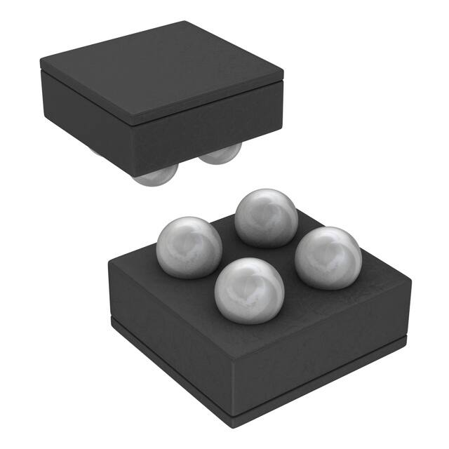
LP5560 is available in TI’s tiny 4-pin DSBGA package
with 0.4-mm pitch.
Device Information(1)
PART NUMBER
LP5560
PACKAGE
DSBGA (4)
BODY SIZE (NOM)
0.886 mm × 0.886 mm
(1) For all available packages, see the orderable addendum at
the end of the data sheet.
Typical Application
VDD
LED
+
-
LP5560
CTRL
GND
Copyright © 2016, Texas Instruments Incorporated
1
An IMPORTANT NOTICE at the end of this data sheet addresses availability, warranty, changes, use in safety-critical applications,
intellectual property matters and other important disclaimers. PRODUCTION DATA.
�LP5560
SNVS873E – AUGUST 2012 – REVISED NOVEMBER 2016
www.ti.com
Table of Contents
1
2
3
4
5
6
7
Features ..................................................................
Applications ...........................................................
Description .............................................................
Revision History.....................................................
Pin Configuration and Functions .........................
Specifications.........................................................
1
1
1
2
3
4
6.1
6.2
6.3
6.4
6.5
6.6
6.7
4
4
4
5
5
6
7
Absolute Maximum Ratings ......................................
ESD Ratings..............................................................
Recommended Operating Conditions.......................
Thermal Information ..................................................
Electrical Characteristics...........................................
Single-Wire Interface Timing Requirements .............
Typical Characteristics ..............................................
Detailed Description .............................................. 8
7.1
7.2
7.3
7.4
Overview ................................................................... 8
Functional Block Diagram ......................................... 8
Feature Description................................................... 9
Device Functional Modes........................................ 17
7.5 Programming .......................................................... 18
7.6 Registers ................................................................. 18
8
Application and Implementation ........................ 19
8.1 Application Information............................................ 19
8.2 Typical Application ................................................. 19
9 Power Supply Recommendations...................... 22
10 Layout................................................................... 22
10.1 Layout Guidelines ................................................. 22
10.2 Layout Example .................................................... 22
11 Device and Documentation Support ................. 23
11.1
11.2
11.3
11.4
11.5
11.6
Documentation Support ........................................
Receiving Notification of Documentation Updates
Community Resources..........................................
Trademarks ...........................................................
Electrostatic Discharge Caution ............................
Glossary ................................................................
23
23
23
23
23
23
12 Mechanical, Packaging, and Orderable
Information ........................................................... 23
4 Revision History
NOTE: Page numbers for previous revisions may differ from page numbers in the current version.
Changes from Revision D (June 2016) to Revision E
•
Page
Changed title of data sheet ................................................................................................................................................... 1
Changes from Revision C (May 2013) to Revision D
Page
•
Added additional Applications, Device Information and Pin Configuration and Functions sections, ESD Ratings and
Thermal Information tables, Feature Description, Device Functional Modes, Application and Implementation, Power
Supply Recommendations, Layout, Device and Documentation Support, and Mechanical, Packaging, and Orderable
Information sections................................................................................................................................................................ 1
•
Changed RθJA value from "120°C/W" to "184.3°C/W"; added additional thermal values ....................................................... 5
Changes from Revision B (April 2013) to Revision C
•
2
Page
Changed layout of National Data Sheet to TI format ........................................................................................................... 18
Submit Documentation Feedback
Copyright © 2012–2016, Texas Instruments Incorporated
Product Folder Links: LP5560
�LP5560
www.ti.com
SNVS873E – AUGUST 2012 – REVISED NOVEMBER 2016
5 Pin Configuration and Functions
YFQ Package
4-Pin DSBGA
Top View
A
VDD
LED
B
GND
CTRL
1
2
Pin Functions
PIN
TYPE (1)
DESCRIPTION
NO.
NAME
A1
VDD
P
Power supply pin
A2
LED
A
Current source output
B1
GND
G
Ground
B2
CTRL
DI
Single-wire interface input
(1)
A: Analog Pin D: Digital Pin G: Ground Pin P: Power Pin I: Input Pin
Submit Documentation Feedback
Copyright © 2012–2016, Texas Instruments Incorporated
Product Folder Links: LP5560
3
�LP5560
SNVS873E – AUGUST 2012 – REVISED NOVEMBER 2016
www.ti.com
6 Specifications
6.1 Absolute Maximum Ratings
over operating free-air temperature range (unless otherwise noted) (1) (2) (3)
MIN
MAX
UNIT
Voltage on VDD pin
−0.3
6
V
Voltage on other pins (CTRL,LED) (4)
−0.3
VDD + 0.3 V with
6 V maximum
V
Continuous power dissipation (5)
Internally Limited
Junction temperature, TJ-MAX
−65
Storage temperature, Tstg
(1)
(2)
(3)
(4)
(5)
125
°C
150
°C
Stresses beyond those listed under Absolute Maximum Ratings may cause permanent damage to the device. These are stress ratings
only, which do not imply functional operation of the device at these or any other conditions beyond those indicated under Recommended
Operating Conditions. Exposure to absolute-maximum-rated conditions for extended periods may affect device reliability.
All voltages are with respect to the potential at the GND pins.
If Military/Aerospace specified devices are required, contact the Texas Instruments Sales Office/ Distributors for availability and
specifications. Voltage
Undervoltage lockout (UVLO) shuts down the LED driver with VIN drops to 2.3 V (typical). Power-on reset (POR) trips at VIN = 2 V
(typical).
Internal thermal shutdown circuitry protects the device from permanent damage. Thermal shutdown engages at TJ = 160°C (typical) and
disengages at TJ=140°C (typical).
6.2 ESD Ratings
VALUE
V(ESD)
(1)
(2)
Electrostatic
discharge
Human-body model (HBM), per ANSI/ESDA/JEDEC JS-001
(1)
±2000
Charged-device model (CDM), per JEDEC specification JESD22-C101 (2)
±1000
UNIT
V
JEDEC document JEP155 states that 500-V HBM allows safe manufacturing with a standard ESD control process.
JEDEC document JEP157 states that 250-V CDM allows safe manufacturing with a standard ESD control process.
6.3 Recommended Operating Conditions
over operating free-air temperature range (unless otherwise noted) (1) (2)
MIN
Voltage on power pin (VDD)
NOM
MAX
UNIT
2.7
5.5
V
Junction temperature, TJ
−30
125
°C
Ambient temperature, TA (1)
−30
85
°C
(1)
(2)
4
In applications where high power dissipation and/or poor package thermal resistance is present, the maximum ambient temperature may
have to be derated. Maximum ambient temperature (TA-MAX) is dependent on the maximum operating junction temperature (TJ-MAX-OP =
125°C), the maximum power dissipation of the device in the application (PD-MAX), and the junction-to ambient thermal resistance of the
part/package in the application (RθJA), as given by the following equation: TA-MAX = TJ-MAX-OP – (RθJA × PD-MAX).
All voltages are with respect to the potential at the GND pin.
Submit Documentation Feedback
Copyright © 2012–2016, Texas Instruments Incorporated
Product Folder Links: LP5560
�LP5560
www.ti.com
SNVS873E – AUGUST 2012 – REVISED NOVEMBER 2016
6.4 Thermal Information
LP5560
THERMAL METRIC (1)
YFQ (DSBGA)
UNIT
4 PINS
RθJA
Junction-to-ambient thermal resistance
RθJC(top)
Junction-to-case (top) thermal resistance
RθJB
Junction-to-board thermal resistance
ψJT
Junction-to-top characterization parameter
ψJB
Junction-to-board characterization parameter
(1)
184.3
°C/W
1.8
°C/W
103.2
°C/W
9.1
°C/W
103.1
°C/W
For more information about traditional and new thermal metrics, see Semiconductor and IC Package Thermal Metrics.
6.5 Electrical Characteristics
Unless otherwise specified: VIN = 3.6 V, CTRL = 3.6 V, VLED = 3.1 V; typical limits are for TA = 25°C, and minimum and
maximum limits apply over the operating ambient temperature range (−30°C < TA < +85°C). (1) (2)
PARAMETER
TEST CONDITIONS
MIN
TYP
MAX
ISD
Shutdown supply current
CTRL = 0 V
0.4
0.75
IQ
Quiescent supply current
ILED = 0 mA
25
30
ILED
LED output current
ISET = 0
2.26
2.8
3.34
ISET = 1 (default)
4.61
5.3
5.99
ISET = 2
6.78
7.8
8.82
ISET = 3
8.87
10.2
11.53
ISET = 4
10.96
12.6
14.24
ISET = 5
13.5
15.0
16.5
ISET = 6
15.05
17.3
19.55
ISET = 7
16.96
19.5
22.04
2.7 V ≤ VIN ≤ 4.5 V
ΔILED%/ΔVIN
Line regulation
ΔILED%/ΔVLED (3)
Load regulation
VHR
Headroom voltage (4)
VIH
Logic input high level
VIN = 2.7 V to 5.5 V
VIL
Logic input low level
VIN = 2.7 V to 5.5 V
ICTRL
CTRL pin leakage current
CTRL = 1.8 V
T_cycle_H
LED On time
T_cycle_L
LED OFF time
IDX = 5.3 mA, Vƒ = 2.5 V
(6)
Trise
LED current rise time
Tfall
LED current fall time (6)
Fade resolution
Rise/fall time resolution
(1)
(2)
(3)
(4)
(5)
(6)
–3%
3%
1.7 V ≤ VLED ≤ 3.4 V, ILED = 5.3 mA
0.6
ILED = 5.3 mA
40
ILED = 19.5 mA
40
Adjustable (5), TA = 25°C
See (5)
UNIT
µA
mA
%/1V
100
1.1
mV
V
0.6
V
400
nA
13.2
3009.6
ms
26.4
6019.2
ms
0
1584
ms
0
1584
ms
105.6
ms
All voltages are with respect to the potential at the GND pins.
Minimum and Maximum limits are specified by design, test, or statistical analysis. Typical numbers are not ensured, but do represent the
most likely norm.
ILED = LED output current, VLED = LED forward voltage.
For LED output pin, headroom voltage is defined as the voltage across the internal current source when the LED current has dropped
10% from the value measured at VIN – 0.5 V. If headroom voltage requirement is not met, LED current regulation is compromised.
Specified by design.
LED current ramp-up and ramp-down uses a combined PWM-current adjustment.
Submit Documentation Feedback
Copyright © 2012–2016, Texas Instruments Incorporated
Product Folder Links: LP5560
5
�LP5560
SNVS873E – AUGUST 2012 – REVISED NOVEMBER 2016
www.ti.com
6.6 Single-Wire Interface Timing Requirements
See
(1) (2)
and Figure 1
MIN
MAX
UNIT
TC_ON
Command pulse on time
15
µs
TC_OFF
Command pulse off time
30
µs
TT_ON
Minimum training pulse on time (3)
200
µs
TT_OFF
Minimum training pulse off time (4)
200
µs
TCAL
Calibration pulse length
0.35
T ENTER
Command entering period
500
T ENTER+T BLANK
Command entering period + Blank period
(1)
(2)
(3)
(4)
8
ms
µs
1500
µs
Specified by design.
Minimum and Maximum limits are specified by design, test, or statistical analysis. Typical numbers are not ensured, but do represent the
most likely norm.
All CTRL signal high times between calibration pulse and training end are considered as training pulse on times.
All CTRL signal low times between calibration pulse and training end are considered as training pulse off times.
TC_ON
TCAL
CTRL
TT_OFF
C
TC_OFF
TENTER
I
R1
TT_ON
TBLANK
TENTER
Figure 1. Interface Timing
6
Submit Documentation Feedback
Copyright © 2012–2016, Texas Instruments Incorporated
Product Folder Links: LP5560
�LP5560
www.ti.com
SNVS873E – AUGUST 2012 – REVISED NOVEMBER 2016
6.7 Typical Characteristics
TJ = 25°C. Unless otherwise noted, typical characteristics apply to the Functional Block Diagram with: VIN = 3.6 V, RISET =
24 kΩ, CIN = 100 nF.
50
QUIESCENT CURRENT ( A)
SHUTDOWN CURRENT ( A)
1.0
0.8
0.6
+25°C
+85°C
0.4
-30°C
0.2
0.0
45
40
30
3.0
3.5 4.0 4.5 5.0
INPUT VOLTAGE (V)
5.5
6.0
+25°C
20
15
10
5
2.5
Figure 2. Standby Current vs VIN
3.0
3.5 4.0 4.5 5.0 5.5
INPUT VOLTAGE (V)
6.0
Figure 3. Quiescent Current vs VIN
6.6
23
6.3
22
6.0
5.7
+85°C
LED CURRENT (mA)
LED CURRENT (mA)
+85°C
25
0
2.5
5.4
5.1
-30°C
4.8
+25°C
4.5
4.2
3.6
2.5
21
+85°C
20
19
-30°C
18
+25°C
17
16
3.9
15
3.0
3.5 4.0 4.5 5.0 5.5
INPUT VOLTAGE (V)
6.0
2.5
5 mA
3.0
3.5 4.0 4.5 5.0 5.5
INPUT VOLTAGE (V)
6.0
20 mA
Figure 4. LED Current vs Input Voltage
Figure 5. LED Current vs Input Voltage
25.0
7
22.5
LED CURRENT (mA)
6
LED CURRENT (mA)
-30°C
35
5
4
3
2
20.0
17.5
15.0
12.5
10.0
7.5
5.0
1
2.5
0.0
0
0.0
0.1
0.2
0.3
0.4
HEADROOM VOLTAGE (V)
0.5
5 mA
0.0
0.1
0.2
0.3
0.4
HEADROOM VOLTAGE (V)
0.5
20 mA
Figure 6. IOUT vs Headroom Voltage
Figure 7. IOUT vs Headroom Voltage
Submit Documentation Feedback
Copyright © 2012–2016, Texas Instruments Incorporated
Product Folder Links: LP5560
7
�LP5560
SNVS873E – AUGUST 2012 – REVISED NOVEMBER 2016
www.ti.com
7 Detailed Description
7.1 Overview
The LP5560 is a programmable LED driver with a single-wire interface. It is designed to drive a single indicator
LED with different blinking sequences. Up to three pulses with different on and off times can be programmed into
the device. LED current rise and fall times can also be independently controlled. Blinking sequence is stored into
volatile memory, thus removing input voltage VIN resets the memory into default state.
The high-side LED driver has very low headroom voltage requirement and can drive most indicator LEDs directly
from battery voltage. A single CTRL pin is used to control the device on and off and to change settings of the
device. A default blinking sequence is programmed into the LP5560 to enable use of the devices in simply
applications without programming capabilities.
7.2 Functional Block Diagram
VDD
POR
CTRL
UVLO
State Machine
LED CONTROL
Single-Wire
Interface
Volatile
Program Memory
OSCILLATOR
IBIAS
BANDGAP
TSD
LED
Default Sequence
GND
Copyright © 2016, Texas Instruments Incorporated
8
Submit Documentation Feedback
Copyright © 2012–2016, Texas Instruments Incorporated
Product Folder Links: LP5560
�LP5560
www.ti.com
SNVS873E – AUGUST 2012 – REVISED NOVEMBER 2016
7.3 Feature Description
7.3.1 LED Driver Headroom Voltage
The current source is connected internally between the VDD and LED output pins. The voltage across the
current source, (VVDD − VLED), is referred as headroom voltage (VHR). The current source requires a sufficient
amount of headroom voltage to be present across it in order to regulate the output current properly. The LP5560
headroom voltage requirement is 40 mV (typical) and does not depend on the current setting.
7.3.2 Single-Wire Interface
The LP5560 has one digital control input (CTRL). Threshold levels of CTRL input are fixed to support control
from low-voltage controller. The CTRL signal is used to control the mode of the circuit. The rising edge of the
CTRL signal activates the circuit and starts a command entering period. During the command entering period all
rising edges are counted. After command entering period there is a blank period when no rising edges are
allowed. If there are any rising edges during blank period these are not detected. User must take care not to start
the training sequence before blank period has elapsed or the training sequence is corrupted.
If CTRL is left high after command entering period, the consequent command is performed right after the blank
period. In case of run once command CTRL pin can be set low after the command entering period and execution
of the command starts once CTRL pin is pulled high after blank period.
CTRL
LED
Command
entering
period
Blank
period
Command
execution
starts
Figure 8. Single-Wire Interface
The LP5560 has four different commands. Command depends on the number of rising edges during command
entering period. If there are more than 4 rising edges during command entering period command is ignored. Note
that even in this case blank period needs to elapse before next command can be given.
Table 1. LP5560 Commands
COMMAND
NUMBER OF RISING EDGES DURING COMMAND
ENTERING PERIOD
Run
1
Training start
2
Training end
3
Run once
4
Submit Documentation Feedback
Copyright © 2012–2016, Texas Instruments Incorporated
Product Folder Links: LP5560
9
�LP5560
SNVS873E – AUGUST 2012 – REVISED NOVEMBER 2016
www.ti.com
7.3.2.1 Run Command
One rising edge of the CTRL signal within command entering period is interpreted as a run command. The CTRL
pin must be kept high during blank period. If the CTRL pin is pulled low during command entering period or blank
period device goes to stand by. In run mode (mode bit = 1) blinking sequence is started right after Blank period
and it is repeated as long as CTRL signal is kept high. When the CTRL signal is set low device goes into standby
mode (Figure 9).
CTRL
To Standby
LED
Command
entering
period
Blank
period
Programmed
sequence
Figure 9. Run Mode
In follow mode (mode bit = 0) LED is turned on right after a blank period, and it stays on as long as CTRL is kept
high. When CTRL signal is set low LED is turned off and device goes into standby mode (Figure 10).
CTRL
To Standby
LED
Command
entering
period
Blank
period
Figure 10. Follow Mode
7.3.2.2 Training Start Command
Two rising edges of CTRL signal within command entering period is interpreted as training start command.
Training start command starts training sequence. Different blinking sequences can be trained into device in
training mode. Training mode is described in more details in Training Mode.
7.3.2.3 Training End Command
Three rising edges of CTRL signal within command entering period is interpreted as training end command.
Training end is used to stop the training sequence.
7.3.2.4 Run-Once Command
Four rising edges of the CTRL signal within command entering period is interpreted as a run-once command.
Programmed blinking sequence is performed once after a run-once command. If CTRL is kept high after
command entering period the programmed blinking sequence starts right after the blank period has elapsed
(Figure 11). The CTRL signal must stay high as long as programmed blinking sequence is executed. If CTRL is
set low during execution of blinking sequence, device goes to standby and execution of blinking sequence is
stopped.
10
Submit Documentation Feedback
Copyright © 2012–2016, Texas Instruments Incorporated
Product Folder Links: LP5560
�LP5560
www.ti.com
SNVS873E – AUGUST 2012 – REVISED NOVEMBER 2016
CTRL
To Standby
Programmed
sequence
LED
Command
entering
period
Blank
period
Figure 11. Run-Once Command
If CTRL signal is low after command entering period, blinking sequence is executed once the CTRL is set high
(Figure 12).
CTRL
To Standby
Programmed
sequence
LED
Command
entering
period
Blank
period
Figure 12. Delayed Run-Once Command
If device is in follow mode (mode bit is 0) the run-once command turns the LED on, and it is kept on as long as
CTRL is held high.
7.3.3 Training Mode
Figure 17 shows an example of a full training sequence with three pulses. Training mode starts with a training
start command. Training start command is followed by blank time during which no rising edges are allowed.
Blank time is followed by calibration pulse. Calibration pulse length (TCAL) defines the speed of the training
sequence and can vary from 350 µs to 8 ms. During parameter settings register values are incremented at speed
defined by TCAL. For example, if calibration pulse length is 1 ms and current setting pulse length is 3.3 ms, the
current-setting value is 3 (current-set register is incremented 3 times). If the parameter-setting pulse is shorter
than the calibration pulse, then the corresponding parameter is set to 0.
The next rising edge after calibration pulse starts LED driver current setting (I). LED driver current is recorded
once CTRL is pulled low. Note that there are empty low times before and after current setting pulse. For the
following pulses both CTRL high and CTRL low times are used to set the parameters. Next the CTRL high time
defines the LED current rise time setting for pulse 1 (R1). When R1 setting is started mode bit is set to 0. This
sets the LP5560 device into follow mode. Mode bit is set to 1 after first off time has been saved into register. This
means that at least one full pulse must be trained into memory to set the device into run mode.
CTRL low time after R1 defines the LED on time for pulse 1 (ON1). CTRL high time after ON1 sets the LED
current fall time (F1). CTRL low time after F1 sets pulse 1 off time (OFF1). Once rising edge of CTRL is detected
after first off time setting mode bit is set to 1 (run mode) and the number of pulses register (NOP[1:0]) is set to 1.
This indicates that one full pulse has been trained into memory.
Rise, on, fall, and off times for pulse 2 and 3 are set the same way as for pulse 1. Note that NOP register is
always incremented after OFFx time setting. This means that all pulse parameters (rise, on, fall, and off times)
must be trained for each pulse make it valid. The training sequence is ended with training end command.
Submit Documentation Feedback
Copyright © 2012–2016, Texas Instruments Incorporated
Product Folder Links: LP5560
11
�LP5560
SNVS873E – AUGUST 2012 – REVISED NOVEMBER 2016
www.ti.com
7.3.3.1 Ending the Training Sequence
A training end command can be given at any time of the training sequence except during blank time. Outcome of
the training sequence depends on the place of the training end command. If a training end command is given
after any of the off-time setting (OFF1, OFF2 or OFF3), mode bit is set to 1, and the corresponding number of
pulses are stored into memory. If a training end command is given after any of the other pulse parameters (Rx,
ONx or Fx) that pulse is ignored. For example, if training end command is given after ON2 pulse 2 is ignored and
blinking sequence includes only pulse 1.
7.3.3.2 Reset to Default
If a training end command is given right after a training start command, the LP5560 is reset back to factory
defaults (Figure 13). In this case the mode bit is set to 1 (run mode) with the factory-set default blinking
sequence.
Training start
command
Training
end
command
Blank period
CTRL
Figure 13. Reset to Default
7.3.3.3 Changing the LED Current
The LP5560 devices allows changing the LED output current without the need to reprogram the previously
programmed blinking sequence. This is done by giving the training end command after current setting
(Figure 14). In this case only the current setting changes. If a blinking sequence was programmed into the
LP5560 device it remains unchanged. If mode bit was 0 (follow mode) before the training sequence it remains 0.
Training
start
command
Training
end
command
Blank
Period
CTRL
C
I
Figure 14. Current Programming Sequence
7.3.3.4 Entering Follow Mode
Mode bit can be set to 0 (follow mode) in two ways. If training end command is given after calibration pulse mode
bit is set to 0 (follow mode) and the previously set LED output current setting remains unchanged (Figure 15).
Training
start
command
CTRL
Training
end
command
Blank
Period
C
Figure 15. Entering Follow Mode
If training end command is given after R1, ON1 or F1 mode bit is set to 0 (follow mode) and new current setting
is stored to current register (Figure 16). If a training end command is given after F1 CTRL low time before
training end command needs to be less than minimum training pulse off time (200 µs). Otherwise off time OFF1
is set to minimum value, and pulse 1 is stored into memory.
12
Submit Documentation Feedback
Copyright © 2012–2016, Texas Instruments Incorporated
Product Folder Links: LP5560
�LP5560
www.ti.com
SNVS873E – AUGUST 2012 – REVISED NOVEMBER 2016
Training
Blank
start
period
command
CTRL
Training
end
command
C
I
R1
Figure 16. Entering Follow Mode With New Current Setting
7.3.3.5 Timeout
If during training CTRL stays constant for more than 127 × TCAL time this is interpreted as timeout. For example,
if calibration pulse length TCAL is 1 ms, timeout time is 127 ms. Timeout ends the training sequence. Timeout is
considered as a false training, and it is a good practice to always give a complete training sequence after timeout
to ensure correct data is stored into memory.
Training
Blank
start
period
command
CTRL
Training
end
command
C
R1 ON1 F1 OFF1 R2
I
ON2
F2
OFF2
R3
ON3
F3
OFF3
Figure 17. Full Training Sequence
7.3.4 LED Output Current Setting
The LED output current can be set from 2.8 mA to 19.5 mA in 7 steps. Duration of the current setting pulse (I)
defines the current setting.
Table 2. LED Current Setting
CURRENT SETTING
LED CURRENT (mA)
0
2.8
1
5.3 default
2
7.8
3
10.2
4
12.6
5
15.0
6
17.3
7
19.5
Submit Documentation Feedback
Copyright © 2012–2016, Texas Instruments Incorporated
Product Folder Links: LP5560
13
�LP5560
SNVS873E – AUGUST 2012 – REVISED NOVEMBER 2016
www.ti.com
7.3.5 Rise and Fall Time Settings
Rise and fall times of each pulse can be programmed independently. Rise and fall time can be set from 0 to
1584 ms with 105.6 ms steps. Rise and fall times are generated using a combined PWM and current control.
Ramp has 32 PWM steps. For the first 8 steps LED current is decreased to 12.5%. For the remaining steps
current is set to 100%. Each step is 3.3 ms long. This results in the minimum ramp time of 3.3 ms × 32 = 105.6
ms. When ramp time is increased each PWM step is done multiple times. When setting rise and fall times they
are always rounded down. For example if calibration pulse length is 1 ms and rise time setting pulse is 2.9 ms
rise time is set to 2 which is 211.2 ms. Rise and fall times can be set to zero by giving pulse that is shorter than
calibration pulse.
Table 3. Rise and Fall Time Settings
RAMP SETTING
14
RAMP TIME (ms)
0
0
1
105.6
2
211.2
3
316.8
4
422.4
5
528 default
6
633.6
7
739.2
8
844.8
9
950.4
10
1056
11
1161.6
12
1267.2
13
1372.8
14
1478.4
15
1584
Submit Documentation Feedback
Copyright © 2012–2016, Texas Instruments Incorporated
Product Folder Links: LP5560
�LP5560
www.ti.com
SNVS873E – AUGUST 2012 – REVISED NOVEMBER 2016
7.3.6 LED ON-Time Setting
LED on time has 5-bit control. On time can be controlled from 13.2 ms to 3009.6 ms in 31 steps. Step size is not
constant to increase resolution on shorter ON times. With longer on times also the step size is increased. Table 4
shows the available on times.
Table 4. LED ON-Time Setting
SETTING
LED ON TIME (ms)
0
13.2
1
26.4
2
52.8
3
105.6
4
158.4
5
211.2
6
264
7
316.8
8
369.6
9
435.6
10
501.6 default
11
594
12
699.6
13
805.2
14
910.8
15
1016.4
16
1122
17
1227.6
18
1353
19
1478.4
20
1603.8
21
1729.2
22
1854.6
23
1980
24
2105.4
25
2230.8
26
2356.2
27
2481.6
28
2613.6
29
2745.6
30
2877.6
31
3009.6
Submit Documentation Feedback
Copyright © 2012–2016, Texas Instruments Incorporated
Product Folder Links: LP5560
15
�LP5560
SNVS873E – AUGUST 2012 – REVISED NOVEMBER 2016
www.ti.com
7.3.7 LED OFF-Time Setting
LED off time has also 5-bit control. Off time can be controlled from 26.4 ms to 6019.2 ms in 31 steps. Off time is
always twice as long as on time with same setting.
Table 5. LED OFF-Time Setting
16
SETTING
LED OFF TIME (ms)
0
26.4
1
52.8
2
105.6
3
211.2
4
316.8
5
422.4
6
528
7
633.6
8
739.2
9
871.2
10
1003.2
11
1188
12
1399.2
13
1610.4 default
14
1821.6
15
2032.8
16
2244
17
2455.2
18
2706
19
2956.8
20
3207.6
21
3458.4
22
3709.2
23
3960
24
4210.8
25
4461.6
26
4712.4
27
4963.2
28
5227.2
29
5491.2
30
5755.2
31
6019.2
Submit Documentation Feedback
Copyright © 2012–2016, Texas Instruments Incorporated
Product Folder Links: LP5560
�LP5560
www.ti.com
SNVS873E – AUGUST 2012 – REVISED NOVEMBER 2016
7.4 Device Functional Modes
POWER-ON RESET When input voltage is applied to VDD pin device goes through power on reset (POR).
During POR defaults are set into control registers.
STANDBY: After POR device goes to standby. This is the low power mode when all the internal blocks are shut
down.
COMMAND ENTERING PERIOD + BLANK PERIOD: Rising edge of the CTRL signal activates the circuit and
starts a command entering period. During the command entering period all rising edges are
counted. After command entering period there is a blank period when no rising edges are allowed.
RUN:
If mode bit is 1 (run mode) and run command has been detected device goes into run mode. In run
mode LP5560 generates the programmed blinking sequence.
FOLLOW MODE: If mode bit is 0 (follow mode) and run command or run once command has been detected
LP5560 goes into follow mode. In follow mode LED stays on as long as CTRL pin is held high.
RUN-ONCE MODE: If run once command has been detected and mode bit is 1 (run mode) device goes into
run-once mode. In run-once mode LP5560 generates the programmed blinking sequence once.
CTRL must be high as long as blinking sequence is running.
TRAINING: If training start command has been detected device goes into training mode. In training mode a
new blinking sequence can be programmed into the device.
Power On Reset
Stand By
Rising edge at CTRL
CTRL = LOW
CTRL = LOW
Run Mode
Follow Mode
Training end
or timeout
Command
entering
period
+
Blank period
CTRL = LOW
Training
Start
Command
Run
Command,
Mode = 1
Run Command
or Run Once
Command,
Mode = 0
CTRL = High
Mode = 0
Run Once
Command,
CTRL = low,
Wait for CTRL
Run Once
Command,
CTRL = High,
Mode = 1
Training Mode
Run Once Mode
CTRL = High
Mode = 1
Submit Documentation Feedback
Copyright © 2012–2016, Texas Instruments Incorporated
Product Folder Links: LP5560
17
�LP5560
SNVS873E – AUGUST 2012 – REVISED NOVEMBER 2016
www.ti.com
7.5 Programming
7.5.1 Default Sequence
Default blinking sequence is programmed into the LP5560 to enable the use of a device in simple systems
without programming capabilities. Default sequence has a single pulse with parameters as follows:
I = 5.3 mA; R1 = 528 ms; ON1 = 501.6 ms; F1 = 528; OFF1 = 1610.4 ms
7.6 Registers
7.6.1 Control Registers
Control registers are shown only for a reference. There is no direct way to write or read these registers. Register
values are set in the training mode as described earlier in the document.
Table 6. Control Registers
7
6
MODE
18
5
4
3
2
1
F1[3:0]
R1[3:0]
F2[3:0]
R2[3:0]
F3[3:0]
R3[3:0]
NOP[1:0]
0
ON1[4:0]
I_LED[2:0]
OFF1[4:0]
n/a
ON2[4:0]
n/a
OFF2[4:0]
n/a
ON3[4:0]
n/a
OFF3[4:0]
Submit Documentation Feedback
Copyright © 2012–2016, Texas Instruments Incorporated
Product Folder Links: LP5560
�LP5560
www.ti.com
SNVS873E – AUGUST 2012 – REVISED NOVEMBER 2016
8 Application and Implementation
NOTE
Information in the following applications sections is not part of the TI component
specification, and TI does not warrant its accuracy or completeness. TI’s customers are
responsible for determining suitability of components for their purposes. Customers should
validate and test their design implementation to confirm system functionality.
8.1 Application Information
The LP5560 is a programmable LED driver designed to generate variety of blinking sequences for indicator
LEDs. It can drive single LED with up to 19.5 mA output current. Very low headroom voltage allows driving most
indicator LEDs straight from a single Li-ion battery. Default blinking sequence with one pulse is programmed into
the LP5560 to enable the use of device in simple systems without programming capabilities. Pulling CTRL signal
high starts the default blinking sequence. Different blinking sequences with up to three pulses can be
programmed into the LP5560 through a single-wire interface. Programmable parameters include on and off times
as well as rise and fall times.
8.2 Typical Application
A1
VIN = 2.7 V to 5.5 V
VDD
LED
A2
ILED = 2.8 mA to 19.5 mA
LP5560
CTRL
B2
CTRL
GND
B1
Copyright © 2016, Texas Instruments Incorporated
Figure 18. LP5560 Typical Application
8.2.1 Design Requirements
In this example LP5560 is used to drive a blue 0406-size indicator LED with a 5.3-mA output current. For this
example, use the parameters listed in Table 7.
Table 7. Design Parameters
DESIGN PARAMETER
EXAMPLE VALUE
LED Output Current
5.3 mA
Maximum LED forward voltage at 5 mA
3.1 V
VIN voltage
from 3.2 V to 5.5 V
8.2.2 Detailed Design Procedure
8.2.2.1 Step-by-Step Design Procedure
To design in the LP5560 use the following simple design steps:
• Define the input voltage range of the system. For the LP5560 device the maximum input voltage must not
exceed 5.5 V. The minimum input voltage is critical parameter for LED selection.
• Define the LED current. LED current affects the LED forward voltage and must be taken into account when
selecting the LED for the application.
• Choose a LED which maximum forward voltage with desired LED current is less than minimum input voltage 100 mV. This ensures that there is always enough headroom voltage available for the LED driver.
Submit Documentation Feedback
Copyright © 2012–2016, Texas Instruments Incorporated
Product Folder Links: LP5560
19
�LP5560
SNVS873E – AUGUST 2012 – REVISED NOVEMBER 2016
www.ti.com
8.2.2.2 Running the Default Blinking Sequence
To run the default blinking sequence apply input voltage to VDD pin. Allow the VDD voltage settle before pulling
the CTRL pin high. It is not recommended to connect the CTRL and VDD lines together. When CTRL line is
pulled high the LP5560 starts to generate the default blinking sequence. Figure 19 shows the LP5560 generating
default sequence. Rise and fall times are generated using a combined PWM and current control. Ramp has 32
PWM steps. For the first 8 steps LED current is decreased to 12.5%. For the remaining steps current is set to
100%. Each step is 3.3 ms long. This result’s the minimum ramp time of 3.3 ms × 32 = 105.6 ms. Figure 22
shows LED current with minimum rise time. When ramp time is increased each PWM step is done multiple times.
In the default sequence rise and fall times are set to 528 ms.
8.2.2.3 Programming New Blinking Sequence to the Memory
Figure 22 shows an example of a training sequence which programs a new blinking sequence into the LP5560
memory. This example has a single pulse with 105.6 ms rise time, 105.6 ms on time, 105.6 ms fall time and
211.2 ms off time. LED current is set to 5.3 mA. Training sequence is started by giving a training start command
(two rising edges within 500 µs). First pulse after a training start command is the calibration pulse which
determines the speed of the training sequence. Note that there must always be at least 1500 µs from the first
rising edge of the training start command before calibration pulse can be given. Second pulse after the
calibration pulse is the LED current setting. Note that there are empty low times before and after current setting
pulse. For the following pulses both CTRL high and CTRL low times are used to set the parameters. Next CTRL
high time defines LED current rise time setting for pulse 1 (R1). CTRL low time after R1 defines the LED on time
for pulse 1 (ON1). CTRL high time after ON1 sets the LED current fall time (F1). CTRL low time after F1 sets
pulse 1 off time (OFF1). The training sequence is finished with a training stop command (three rising edges
within 500 µs). Figure 23 show the LED current after programming the new pulse into the LP5560 memory.
Figure 24 and Figure 25 show another example of a training sequence with three pulses and the resulting
blinking sequence. In this example all three pulses have different rise, on, fall, and off times. LED current is set to
10.2 mA. Figure 26 show how this sequence is run only once using the run-once command. Even though the
CTRL is held high for a long time the blinking sequence is only executed one time because a run-once command
(four rising edges within 500 µs) is given at the beginning of the frame.
8.2.3 Application Curves
Figure 19. Default Blinking Sequence
20
Submit Documentation Feedback
Figure 20. LED Rise Time Set to 105.6 ms
Copyright © 2012–2016, Texas Instruments Incorporated
Product Folder Links: LP5560
�LP5560
www.ti.com
SNVS873E – AUGUST 2012 – REVISED NOVEMBER 2016
Figure 21. LED Rise Time Set to 0 ms
Figure 22. Example Training Sequence with One Pulse
Figure 23. Example Blinking Sequence with One Pulse
Figure 24. Example Training Sequence with Three Pulses
Figure 25. Example Blinking Sequence with Three Pulses
Figure 26. Run-Once Command
Submit Documentation Feedback
Copyright © 2012–2016, Texas Instruments Incorporated
Product Folder Links: LP5560
21
�LP5560
SNVS873E – AUGUST 2012 – REVISED NOVEMBER 2016
www.ti.com
9 Power Supply Recommendations
The LP5560 is designed to operate from an input voltage supply range between 2.7 V and 5.5 V. This input
supply must be well regulated. If the input voltage has high noise content TI recommends adding a dedicated
ceramic bypass capacitor close to the VDD and GND pins. Depending on the selected LED it may be necessary
to increase the minimum input voltage. The minimum input voltage must always be 100 mV higher than the LED
maximum forward voltage.
10 Layout
10.1 Layout Guidelines
•
•
•
•
Normally the LP5560 device does not require any external components except for the LED. However, in a
noisy environment a small 0.1-µF bypass capacitor can be connected between VIN and GND pins.
TI recommends routing the pins in a 45-degree angle to avoid component rotation during soldering process.
Use traces with similar width for all pins. This makes the exposed copper area similar for all pins and
improves the soldering reliability.
Obtain the minimum clearance and trace width from the manufacturer of the PCB used for the board.
10.2 Layout Example
VIA to VDD
Optional
bypass capacitor
VIA to GND
VDD
LED
GND
CTRL
0.1 F
To control
signal
VIA to
GND
Figure 27. LP5560 Layout Example
22
Submit Documentation Feedback
Copyright © 2012–2016, Texas Instruments Incorporated
Product Folder Links: LP5560
�LP5560
www.ti.com
SNVS873E – AUGUST 2012 – REVISED NOVEMBER 2016
11 Device and Documentation Support
11.1 Documentation Support
11.1.1 Related Documentation
For additional information, see the following:
AN-1112 DSBGA Wafer Level Chip Scale Package
11.2 Receiving Notification of Documentation Updates
To receive notification of documentation updates, navigate to the device product folder on ti.com. In the upper
right corner, click on Alert me to register and receive a weekly digest of any product information that has
changed. For change details, review the revision history included in any revised document.
11.3 Community Resources
The following links connect to TI community resources. Linked contents are provided "AS IS" by the respective
contributors. They do not constitute TI specifications and do not necessarily reflect TI's views; see TI's Terms of
Use.
TI E2E™ Online Community TI's Engineer-to-Engineer (E2E) Community. Created to foster collaboration
among engineers. At e2e.ti.com, you can ask questions, share knowledge, explore ideas and help
solve problems with fellow engineers.
Design Support TI's Design Support Quickly find helpful E2E forums along with design support tools and
contact information for technical support.
11.4 Trademarks
E2E is a trademark of Texas Instruments.
All other trademarks are the property of their respective owners.
11.5 Electrostatic Discharge Caution
This integrated circuit can be damaged by ESD. Texas Instruments recommends that all integrated circuits be handled with
appropriate precautions. Failure to observe proper handling and installation procedures can cause damage.
ESD damage can range from subtle performance degradation to complete device failure. Precision integrated circuits may be more
susceptible to damage because very small parametric changes could cause the device not to meet its published specifications.
11.6 Glossary
SLYZ022 — TI Glossary.
This glossary lists and explains terms, acronyms, and definitions.
12 Mechanical, Packaging, and Orderable Information
The following pages include mechanical, packaging, and orderable information. This information is the most
current data available for the designated devices. This data is subject to change without notice and revision of
this document. For browser-based versions of this data sheet, refer to the left-hand navigation.
Submit Documentation Feedback
Copyright © 2012–2016, Texas Instruments Incorporated
Product Folder Links: LP5560
23
�PACKAGE OPTION ADDENDUM
www.ti.com
10-Dec-2020
PACKAGING INFORMATION
Orderable Device
Status
(1)
Package Type Package Pins Package
Drawing
Qty
Eco Plan
(2)
Lead finish/
Ball material
MSL Peak Temp
Op Temp (°C)
(3)
Device Marking
(4/5)
(6)
LP5560TME/NOPB
ACTIVE
DSBGA
YFQ
4
250
RoHS & Green
SNAGCU
Level-1-260C-UNLIM
-30 to 85
LP5560TMX/NOPB
ACTIVE
DSBGA
YFQ
4
3000
RoHS & Green
SNAGCU
Level-1-260C-UNLIM
-30 to 85
(1)
The marketing status values are defined as follows:
ACTIVE: Product device recommended for new designs.
LIFEBUY: TI has announced that the device will be discontinued, and a lifetime-buy period is in effect.
NRND: Not recommended for new designs. Device is in production to support existing customers, but TI does not recommend using this part in a new design.
PREVIEW: Device has been announced but is not in production. Samples may or may not be available.
OBSOLETE: TI has discontinued the production of the device.
(2)
RoHS: TI defines "RoHS" to mean semiconductor products that are compliant with the current EU RoHS requirements for all 10 RoHS substances, including the requirement that RoHS substance
do not exceed 0.1% by weight in homogeneous materials. Where designed to be soldered at high temperatures, "RoHS" products are suitable for use in specified lead-free processes. TI may
reference these types of products as "Pb-Free".
RoHS Exempt: TI defines "RoHS Exempt" to mean products that contain lead but are compliant with EU RoHS pursuant to a specific EU RoHS exemption.
Green: TI defines "Green" to mean the content of Chlorine (Cl) and Bromine (Br) based flame retardants meet JS709B low halogen requirements of