User's Guide
SNVA188B – November 2006 – Revised April 2013
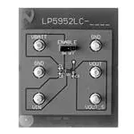
AN-1531 LP5952 Evaluation Board
1
Introduction
This evaluation board is designed to enable independent evaluation of the LP5952 electrical performance.
Each board is pre-assembled and tested in the factory.
The evaluation kits are available in four output voltage options for the DSBGA package: LP5952TL-1.2EV,
LP5952TL-1.3EV, LP5952TL-1.5EV and LP5952TL-1.8EV and one output voltage option for the COL
USON package: LP5952LC-1.5EV. For other voltage options, the device can be ordered from LP5952
product folder on the TI website.
The board contains the LP5952 and input and output capacitors connected to GND.
2
General Description
The LP5952 converts higher input voltages connected to the power input voltage pin VIN to lower output
voltages while consuming low quiescent current. The bias input voltage VBATT supplies internal circuitry.
The LP5952 is capable of operating with input voltage ranges from 0.7V ≤ VIN ≤ 4.5V and 2.5V ≤ VBATT ≤
5.5V for fixed output voltage options from 0.5V to 2.0V. The LP5952 can supply a maximum output current
of 350mA and is particularly suitable for portable, battery-powered systems. It also features internal
protection against short-circuit and over-temperature conditions.
The power input voltage applied between VIN and GND should be at least 0.2V above the output voltage
and the bias input voltage applied between VBATT and GND should be at least 1.5V above the output
voltage (with a minimum of 2.5V) to operate the device within operating conditions. Input connections
should be kept reasonably short (
很抱歉,暂时无法提供与“LP5952TL-1.5EV”相匹配的价格&库存,您可以联系我们找货
免费人工找货