物料型号:LP8340
器件简介:
LP8340是一款低压降(LDO)CMOS线性稳压器,由德州仪器(Texas Instruments)生产。它能够提供高达1.0A的输出电流,并具有低至19µA的典型静态电流。该器件适用于多种应用,包括硬盘驱动器、笔记本电脑、电池供电电子设备和便携式仪器。
引脚分配:
- VIN:输入电压引脚
- VOUT:输出电压引脚
- GND:地线
- ADJ:可调输出版本中的调节引脚
- N/C:无连接引脚
- VOUT Sense:输出电压检测引脚(仅限LLP版本)
参数特性:
- 输出电压公差:±1.5%典型值
- 典型压降电压:在1.0A输出时,5V版本为420mV,3.3V版本为540mV,2.5V版本为670mV,1.8V版本为680mV
- 工作电压范围:2.7V至10V
- 内部1.0A PMOS输出晶体管
- 热过载限制
- 反折限流
- 齐纳校准的带隙基准电压
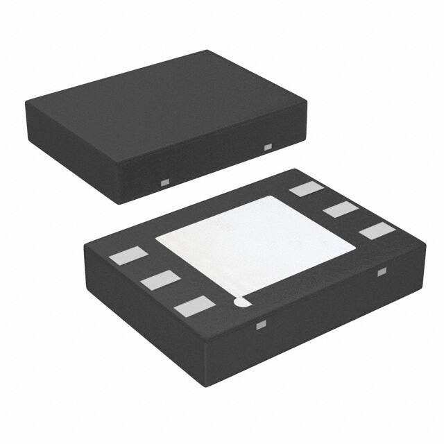
- 封装类型:WSON和PFM
功能详解:
LP8340包括一个齐纳校准的带隙电压基准、反折限流和热过载限流。它采用PMOS输出晶体管,与PNP型低压降调节器不同,不需要基极驱动电流,这使得设备在工作温度、供电电压和负载电流变化时,地线电流保持在50µA以下。
应用信息:
适用于需要高效率和低静态电流的场合,如电池供电设备和便携式设备。
封装信息:
LP8340提供WSON和PFM两种封装选项,其中WSON封装具有更小的占用空间,适合空间受限的应用。
绝对最大额定值:
- 输入电压、输出电压和ADJ引脚:-0.3V至12V
- 存储温度范围:-65°C至160°C
- 结温:150°C
- ESD等级:人体模型2kV,机器模型200V
操作评级:
- 供电电压:2.7V至10V
- 温度范围:LP8340C为0°C至125°C,LP8340I为-40°C至125°C
电气特性:
文档提供了详细的电气特性表,包括输入电压、输出电压、负载调整、线路调整、压降电压、静态电流、最小负载电流、限流、纹波抑制比、热关断温度、调节输入漏电流、输出漏电流和输出噪声等参数的最小值、典型值和最大值。