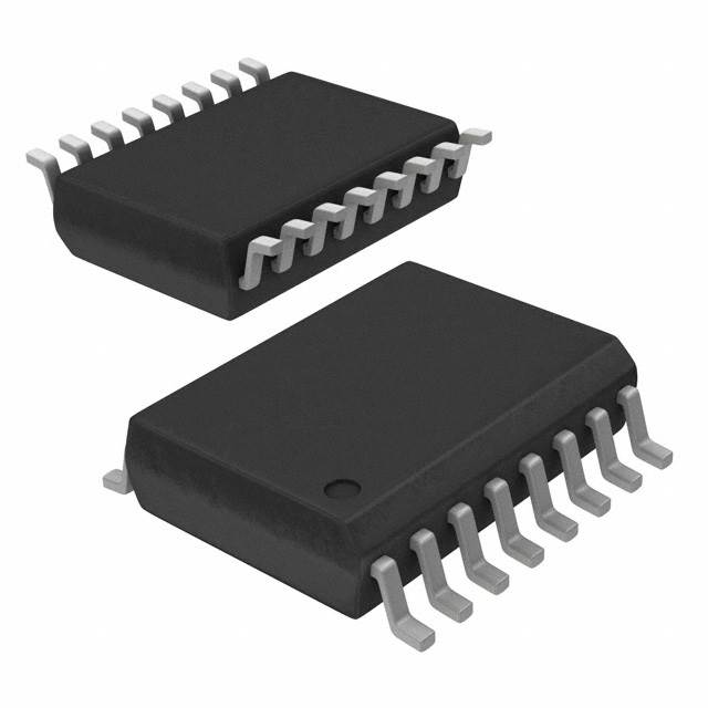
LT1014D-EP
www.ti.com ........................................................................................................................................................................................... SLOS609 – DECEMBER 2008
QUAD PRECISION OPERATIONAL AMPLIFIER
FEATURES
1
•
•
•
•
•
•
•
•
Single-Supply Operation:
Input Voltage Range Extends to Ground, and
Output Swings to Ground While Sinking
Current
Input Offset Voltage 300 mV Max at 25°C
Offset Voltage Temperature Coefficient
2.5 µV/°C Max
Input Offset Current 1.5 nA Max at 25°C
High Gain 1.2 V/µV Min (RL = 2 kΩ),
0.5 V/µV Min (RL = 600 Ω)
Low Supply Current 2.2 mA Max at 25°C
Low Peak-to-Peak Noise Voltage
0.55 µV Typ
Low Current Noise 0.07 pA/√Hz Typ
SUPPORTS DEFENSE, AEROSPACE,
AND MEDICAL APPLICATIONS
•
•
•
•
•
•
•
Controlled Baseline
One Assembly/Test Site
One Fabrication Site
Available in Military (–55°C/125°C)
Temperature Range (1)
Extended Product Life Cycle
Extended Product-Change Notification
Product Traceability
DW PACKAGE
(TOP VIEW)
1OUT
1IN1IN+
VCC+
2IN+
2IN2OUT
NC
(1)
1
16
2
15
3
14
4
13
5
12
6
7
11
10
8
9
4OUT
4IN4IN+
VCC- /GND
3IN+
3IN3OUT
NC
Additional temperature ranges are available - contact factory
DESCRIPTION
The LT1014D is a quad precision operational amplifier with 14-pin industry-standard configuration. It features low
offset-voltage temperature coefficient, high gain, low supply current, and low noise.
The LT1014D can be operated with both dual ±15-V and single 5-V power supplies. The common-mode input
voltage range includes ground, and the output voltage can also swing to within a few milivolts of ground.
Crossover distortion is eliminated.
ORDERING INFORMATION (1)
PACKAGE (2)
TA
–55°C to 125°C
(1)
(2)
SIOC-DW
Reel of 2000
ORDERABLE PART NUMBER
LT1014DMDWREP
TOP-SIDE MARKING
LT1014DMEP
For the most current package and ordering information, see the Package Option Addendum at the end of this document, or see the TI
Web site at www.ti.com.
Package drawings, standard packing quantities, thermal data, symbolization, and PCB design guidelines are available at
www.ti.com/sc/package.
1
Please be aware that an important notice concerning availability, standard warranty, and use in critical applications of Texas
Instruments semiconductor products and disclaimers thereto appears at the end of this data sheet.
PRODUCTION DATA information is current as of publication date.
Products conform to specifications per the terms of the Texas
Instruments standard warranty. Production processing does not
necessarily include testing of all parameters.
Copyright © 2008, Texas Instruments Incorporated
�LT1014D-EP
SLOS609 – DECEMBER 2008 ........................................................................................................................................................................................... www.ti.com
Q24
10 pF
2 kΩ
4 pF
1.3 kΩ
Q20
Q19
2 kΩ
10 pF
Q10
Q11
Submit Documentation Feedback
VCC−
Component values are nominal.
75 pF
Q9
Q7
Q29
Q12
IN+
IN−
400 Ω
400 Ω
Q1
Q21
Q5
Q2
Q22
Q6
Q28
Q27
5 kΩ
Q8
3.9 kΩ
Q4
Q3
Q13
5 kΩ
21 pF
Q18
Q17
2.5 pF
Q15
Q14
Q16
2 kΩ
Q23
Q31
Q26
2.4 kΩ
Q25
Q30
Q32
1 kΩ
100 Ω
1.6 kΩ
1.6 kΩ
1.6 kΩ
9 kΩ
9 kΩ
V CC+
2
30 Ω
42 kΩ
Q34
18 Ω
Q33
Q35
OUT
14 kΩ
Q37
Q40
Q38
600 Ω
Q39
Q41
J1
Q36
800 Ω
SCHEMATIC (EACH AMPLIFIER)
Copyright © 2008, Texas Instruments Incorporated
Product Folder Link(s): LT1014D-EP
�LT1014D-EP
www.ti.com ........................................................................................................................................................................................... SLOS609 – DECEMBER 2008
ABSOLUTE MAXIMUM RATINGS
over operating free-air temperature range (unless otherwise noted)
VCC
VI
(1)
MIN
MAX
supply voltage (2)
–22
22
V
Differential input voltage (3)
–30
30
V
VCC+
V
Input voltage range (any input)
(2)
VCC- – 5
Duration of short-circuit current (4)
TA ≤ 25°C
UNIT
Unlimited
Continuous total power dissipation
See Dissipation Ratings Table
TA
Operating temperature range
–55
125
°C
Tstg
Storage temperature range
–65
150
°C
260
°C
Lead temperature 1,6 mm, at distance 1/16 inch from case for 10s
(1)
(2)
(3)
(4)
Stresses beyond those listed under "absolute maximum ratings" may cause permanent damage to the device. These are stress ratings
only, and functional operation of the device at these or any other conditions beyond those indicated under "recommended operating
conditions" is not implied. Exposure to absolute-maximum-rated conditions for extended periods may affect device reliability.
All voltage values, except differential voltages, are with respect to the midpoint between VCC+ and VCC-.
Differential voltages are at the noninverting input with respect to the inverting input.
The output may be shorted to either supply.
DISSIPATION RATINGS
PACKAGE
TA ≤ 25°c
POWER RATING
DERATING
FACTOR
ABOVE TA = 25°C
TA = 70°C
POWER RATING
TA = 105°C
POWER RATING
TA = 125°C
POWER RATING
DW
1025 mV
8.2 mW/°C
656 mW
369 mW
205 mW
ELECTRICAL CHARACTERISTICS
over operating free-air temperature range, VCC+ = 5 V, VCC- = 0, VO = 1.4 V, VIC = 0 (unless otherwise noted)
PARAMETER
VIO
Input offset voltage
TEST CONDITIONS
RS = 50 Ω
RS = 50 Ω, VIC = 0.1 V
IIO
Input offset current
IIB
Input bias current
VICR
Common-mode input voltage
range
AVD
ICC
Supply current per amplifier
(1)
MAX
90
450
Full range
400
1500
125°C
200
750
25°C
0.2
2
10
25°C
-15
-50
-120
25°C
0 to 3.5
Full range
0.1 to 3
-0.3 to 3.8
15
25
25°C
5
10
18
nA
nA
mV
25°C
Output high, no load
25°C
4
4.4
Output high
25°C
3.4
4
V
Full range
3.1
25°C
1
V/µV
25°C
0.3
VO = 5 mV to 4 V, RL = 500 Ω
Full range
220
µV
V
25°C
Full range
UNIT
Output low, ISINK = 1 mA
RL = 600 Ω to GND
Large-signal differential
voltage amplification
MIN
Full range
Ouput low, RL = 600 Ω to GND
Maximum peak output
voltage swing
TYP
25°C
Full range
Output low, no load
VOM
TA (1)
350
0.5
0.65
mA
Full range is -55°C to 125°C.
Submit Documentation Feedback
Copyright © 2008, Texas Instruments Incorporated
Product Folder Link(s): LT1014D-EP
3
�LT1014D-EP
SLOS609 – DECEMBER 2008 ........................................................................................................................................................................................... www.ti.com
OPERATING CHARACTERISTICS
over operating free-air temperature range, VCC± = 15 V, VIC = 0, TA = 25°C (unless otherwise noted)
PARAMETER
SR
TEST CONDITIONS
Slew rate
MIN
TYP
0.2
0.4
f = 10 Hz
24
f = 1kHz
22
MAX
UNIT
V/µs
Vn
Equivalent input noise voltage
nV/√Hz
VN(PP)
Peak-to-peak equivalent input noise voltage
f = 0.1 Hz to 10 Hz
0.55
µV
In
Equivalent input noise current
f = 10 Hz
0.07
pA/√Hz
TYPICAL CHARACTERISTICS
Table of Graphs
FIGURE
VIO
Input offset voltage vs balanced source resistance
Figure 2
VIO
Input offset voltage vs free-air temperature
Figure 3
Warm-up change in input offset voltage vs elapsed time
Figure 4
IIO
Input offset current vs Input offset current vs free-air temperature
Figure 5
IIB
Input bias current vs free-air temperature
Figure 6
VIC
Common-mode input voltage vs input bias current
ΔVIO
AVD
vs load resistance
Differential voltage amplification
vs frequency
Figure 10 Figure 11
Channel separation vs frequency
Figure 12
Output saturation voltage vs free-air temperature
Figure 13
CMRR
Common-mode rejection ratio vs frequency
Figure 14
kSVR
Supply-voltage rejection ratio vs frequency
Figure 15
ICC
Supply current vs free-air temperature
Figure 16
IOS
Short-circuit output current vs elapsed time
Figure 17
Vn
Equivalent input noise voltage vs frequency
Figure 18
In
Equivalent input noise current vs frequency
Figure 18
Peak-to-peak input noise voltage vs time
Figure 19
VN(PP)
Pulse response (small signal) vs time
Figure 20 Figure 22
Pulse response (large signal) vs time
Figure 21 Figure 23 Figure 24
Phase shift vs frequency
4
Figure 7
Figure 8 Figure 9
Figure 10
Submit Documentation Feedback
Copyright © 2008, Texas Instruments Incorporated
Product Folder Link(s): LT1014D-EP
�LT1014D-EP
www.ti.com ........................................................................................................................................................................................... SLOS609 – DECEMBER 2008
INPUT OFFSET VOLTAGE
OF REPRESENTATIVE UNITS
vs
FREE-AIR TEMPERATURE
INPUT OFFSET VOLTAGE
vs
BALANCED SOURCE RESISTANCE
10
TA = 25°C
250
VCC± = ±15 V
VIO - Input Offset Volta ge - mV
VIO - Input Offset Voltage - mV
200
1
VCC± = 5 V
VCC- = 0
0.1
RS
+
VCC± = ±15 V
0.01
1k
100
50
0
-50
-100
-150
-200
RS
3k
150
10 k 30 k 100 k 300 k 1 M
3 M 10 M
-250
-50
Rs - Sour ce Resistance - Ω
-25
0
25
50
75
100
125
100
125
TA - Free-Air Temperature - °C
Figure 2.
Figure 3.
INPUT OFFSET CURRENT
vs
FREE-AIR TEMPERATURE
WARM-UP CHANGE IN INPUT OFFSET VOLTAGE
vs
ELAPSED TIME
1
VCC± = ±15 V
TA = 25°C
VIC = 0
0.8
4
I IO - Input Offset Current - nA
∆V IO - Chang e in Input Offset Votla ge - mV
5
3
2
N Package
1
0.6
VCC± = ±2.5 V
0.4
VCC+ = 5 V, V CC- = 0
0.2
J Package
VCC± = ±15 V
0
0
1
2
4
3
5
0
-50
t - Time After P ower -On - min
Figure 4.
-25
0
25
50
75
TA - Free-Air Temperature - °C
Figure 5.
Submit Documentation Feedback
Copyright © 2008, Texas Instruments Incorporated
Product Folder Link(s): LT1014D-EP
5
�LT1014D-EP
SLOS609 – DECEMBER 2008 ........................................................................................................................................................................................... www.ti.com
COMMON-MODE INPUT VOLTAGE
vs
INPUT BIAS CURRENT
INPUT BIAS CURRENT
vs
FREE-AIR TEMPERATURE
-30
5
15
VIC = 0
I IB - Input Bias Current - nA
-25
-20
VCC = 5 V, V CC- = 0
-15
VCC± = ±2.5 V
-10
VCC± = ±15 V
-5
4
10
5
3
VCC± = ±15 V
(Left Scale)
-5
1
-10
0
-1
-25
0
25
50
75
100
0
125
-5
-10
-15
-20
-25
-30
IIB - Input Bias Current - nA
TA - Free-Air Temperature - °C
Figure 6.
Figure 7.
DIFFERENTIAL VOLTAGE AMPLIFICATION
vs
LOAD RESISTANCE
DIFFERENTIAL VOLTAGE AMPLIFICATION
vs
LOAD RESISTANCE
10
A VD - Diff erential Voltage Amplivication - V/mV
10
A VD - Diff erential Voltage Amplivication - V/mV
2
-15
0
-50
VCC± = ±15 V
VO = ±10 V
TA = 25°C
4
TA = -55 °C
1
TA = 125°C
0.4
0.1
100
400
1k
RL - Load Resistance -
4k
10 k
VCC+ = 5 V, V CC- = 0
VO = 20 mV to 3.5 V
4
TA = -55 °C
1
TA = 25°C
TA = 125°C
0.4
0.1
100
400
1k
RL - Load Resistance -
Ω
Figure 8.
6
VCC+ = 5 V
VCC- = 0
(Right Scale)
0
VIC - Common-Mode Input Voltage - V
VIC - Common-Mode Input Voltage - V
TA = 25°C
4k
10 k
Ω
Figure 9.
Submit Documentation Feedback
Copyright © 2008, Texas Instruments Incorporated
Product Folder Link(s): LT1014D-EP
�LT1014D-EP
www.ti.com ........................................................................................................................................................................................... SLOS609 – DECEMBER 2008
DIFFERENTIAL VOLTAGE AMPLIFICATION
vs
FREQUENCY
VIC = 0
CL = 100 pF
TA = 25°C
20
VCC± = ±15 V
100°
120°
AVD
VCC+ = 5 V
VCC- = 0
10
140°
160°
VCC+ = 5 V
VCC- = 0
0
180°
200°
VCC± = ±15 V
220°
-10
0.01
0.3
1
A VD - Diff erential Voltage Amplivication - dB
140
80°
φ - Phase Shift
A VD - Diff erential Voltage Amplivication - dB
DIFFERENTIAL VOLTAGE AMPLIFICATION
AND PHASE SHIFT
vs
FREQUENCY
120
100
80
VCC + = 5 V
VCC - = 0
VCC± = ±15 V
60
40
20
0
-20
0.01 0.1
240°
10
3
CL = 100 pF
TA = 25°C
1
10 100 1 k 10 k 100 k 1 M 10 M
f - Frequenc y - Hz
f - Frequenc y - MHz
Figure 10.
Figure 11.
CHANNEL SEPARATION
vs
FREQUENCY
OUTPUT SATURATION VOLTAGE
vs
FREE-AIR TEMPERATURE
10
160
VCC± = ±15 V
VI(PP) = 20 V to 5 kHz
RL = 2 kΩ
TA = 25°C
120
Limited by
Thermal
Interaction
Output Saturation Voltage - V
Channel Separation - dB
140
VCC+ = 5 V to 30 V
VCC- = 0
RL = 100 Ω
RL = 1 kΩ
100
Limited by
Pin-to-Pin
Capacitance
80
Isink = 10 mA
1
Isink = 5 mA
Isink = 1 mA
0.1
Isink = 100 µA
Isink = 10 µA
Isink = 0
60
10
100
1k
10 k
100 k
1M
0.01
-50
-25
0
25
50
75
f - Frequenc y - Hz
TA - Free-Air Temperature - °C
Figure 12.
Figure 13.
100
Submit Documentation Feedback
Copyright © 2008, Texas Instruments Incorporated
Product Folder Link(s): LT1014D-EP
125
7
�LT1014D-EP
SLOS609 – DECEMBER 2008 ........................................................................................................................................................................................... www.ti.com
SUPPLY-VOLTAGE REJECTION RATIO
vs
FREQUENCY
COMMON-MODE REJECTION RATIO
vs
FREQUENCY
140
TA = 25°C
K SVR - Suppl y-Voltage Rejection Ratio - dB
CMRR - Common-Mode Rejection Ratio - dB
120
100
VCC± = ±15 V
VCC+ = 5 V
VCC- = 0
80
60
40
20
0
10
100
1k
100 k
10 k
VCC± = ± 15 V
TA = 25°C
120
100
Positive
Supply
Negative
Supply
80
60
40
20
0
0.1
1M
1k
10 k
Figure 14.
Figure 15.
40
420
380
VCC± = ±15 V
340
VCC+ = 5 V
VCC- = 0
300
100 k
1M
SHORT-CIRCUIT OUTPUT CURRENT
vs
ELAPSED TIME
I OS - Shor t-Circuit Output Current - mA
I CC - Suppl y Current PerAmplifier - mV
100
f - Frequenc y - Hz
460
TA = -55 °C
30
TA = 25°C
20
TA = 125°C
VCC± = ±15 V
10
0
TA = 125°C
-10
TA = 25°C
-20
TA = -55 °C
-30
-40
-25
0
25
50
75
100
125
0
TA - Free-Air Temperature - °C
Figure 16.
8
10
f - Frequenc y - Hz
SUPPLY CURRENT
vs
FREE-AIR TEMPERATURE
260
-50
1
1
2
3
t - Time - min
Figure 17.
Submit Documentation Feedback
Copyright © 2008, Texas Instruments Incorporated
Product Folder Link(s): LT1014D-EP
�LT1014D-EP
www.ti.com ........................................................................................................................................................................................... SLOS609 – DECEMBER 2008
1000
VCC± = ±2 V to ±18 V
TA = 25°C
300
300
In
100
100
Vn
30
30
1/f Corner = 2 Hz
10
1
10
2000
1200
800
400
10
1k
100
VCC± = ±2 V to ±18 V
f = 0.1 Hz to 10 Hz
TA = 25°C
1600
V N(PP) - Noise Voltage - nV
Vn - Equiv alent Input Noise Voltage - fA/ Hz
1000
PEAK-TO-PEAK INPUT NOISE VOLTAGE
OVER A 10-SECOND PERIOD
vs
TIME
I n - Equiv alent Input Noise Current -fA/ Hz
EQUIVALENT INPUT NOISE VOLTAGE
AND EQUIVALENT INPUT NOISE CURRENT
vs
FREQUENCY
0
f - Frequenc y - Hz
0
2
4
6
8
10
t - Time - s
Figure 18.
Figure 19.
VOLTAGE-FOLLOWER SMALL-SIGNAL
PULSE RESPONSE
vs
TIME
80
6
VCC± = ±15 V
AV = 1
TA = 25°C
5
40
V O - Output Voltage - V
V O - Output Voltage - mV
60
VOLTAGE-FOLLOWER LARGE-SIGNAL
PULSE RESPONSE
vs
TIME
20
0
-20
-40
-60
-80
4
VCC+ = 5 V
VCC- = 0
VI = 0 to 4 V
RL = 0
AV = 1
TA = 25°C
3
2
1
0
-1
0
2
4
6
8
10
12
14
-2
t - Time - ms
0
10
20
30
40
50
60
70
t - Time - ms
Figure 20.
Figure 21.
Submit Documentation Feedback
Copyright © 2008, Texas Instruments Incorporated
Product Folder Link(s): LT1014D-EP
9
�LT1014D-EP
SLOS609 – DECEMBER 2008 ........................................................................................................................................................................................... www.ti.com
VOLTAGE-FOLLOWER SMALL-SIGNAL
PULSE RESPONSE
vs
TIME
6
160
VCC+ = 5 V
VCC- = 0
VI = 0 to 100 mV
RL = 600 Ω to GND
AV = 1
TA = 25°C
120
100
5
4
V O - Output Voltage - mV
140
V O - Output Voltage - mV
VOLTAGE-FOLLOWER LARGE-SIGNAL
PULSE RESPONSE
vs
TIME
80
60
40
3
2
1
0
20
-1
0
-20
VCC+ = 5 V
VCC- = 0
VI = 0 to 4 V
RL = 4.7 kΩ to 5 V
AV = 1
TA = 25°C
-2
0
20
40
60
80
0
100 120 140
10 20 30 40
t - Time - ms
t - TIme - ms
Figure 22.
50
60
70
Figure 23.
VOLTAGE-FOLLOWER LARGE-SIGNAL
PULSE RESPONSE
vs
TIME
6
V O - Output Voltage - V
5
4
VCC+ = 5 V
VCC- = 0
VI = 0 to 4 V
RL = 0
AV = 1
TA = 25°C
3
2
1
0
-1
-2
0
10
20
30
40
50
60
70
t - Time - ms
Figure 24.
10
Submit Documentation Feedback
Copyright © 2008, Texas Instruments Incorporated
Product Folder Link(s): LT1014D-EP
�LT1014D-EP
www.ti.com ........................................................................................................................................................................................... SLOS609 – DECEMBER 2008
APPLICATION INFORMATION
SINGLE-SUPPLY OPERATION
The LT1014D is fully specified for single-supply operation (VCC- = 0). The common-mode input voltage range
includes ground, and the output swings within a few millivolts of ground.
Furthermore, the LT1014D has specific circuitry that addresses the difficulties of single-supply operation, both at
the input and at the output. At the input, the driving signal can fall below 0 V, either inadvertently or on a
transient basis. If the input is more than a few hundred millivolts below ground, the LT1014D is designed to deal
with the following two problems that can occur:
1. On many other operational amplifiers, when the input is more than a diode drop below ground, unlimited
current flows from the substrate (VCC- terminal) to the input, which can destroy the unit. On the LT1014D, the
400-Ω resistors in series with the input (see schematic) protect the device even when the input is 5 V below
ground.
2. When the input is more than 400 mV below ground (at TA = 25°C), the input stage of similar type operational
amplifiers saturates, and phase reversal occurs at the output. This can cause lockup in servo systems.
Because of unique phase-reversal protection circuitry (Q21, Q22, Q27, and Q28), the LT1014D outputs do
not reverse, even when the inputs are at -1.5 V (see Figure 25).
However, this phase-reversal protection circuitry does not function when the other operational amplifier on the
LT1014D is driven hard into negative saturation at the output. Phase-reversal protection does not work on an
amplifier:
• When 4's output is in negative saturation (the outputs of 2 and 3 have no effect)
• When 3's output is in negative saturation (the outputs of 1 and 4 have no effect)
• When 2's output is in negative saturation (the outputs of 1 and 4 have no effect)
• When 1's output is in negative saturation (the outputs of 2 and 3 have no effect)
At the output, other single-supply designs either cannot swing to within 600 mV of ground or cannot sink more
than a few microproamperes while swinging to ground. The all-npn output stage of the LT1014D maintains its low
output resistance and high gain characteristics until the output is saturated. In dual-supply operations, the output
stage is free of crossover distortion.
V O − Output Voltage − V
V I(PP) − Input Voltage − V
4
3
2
1
0
−1
−2
5
V O − Output Voltage − V
5
5
4
3
2
1
0
−1
(a) VI(PP) = −1.5 V to 4.5 V
4
3
2
1
0
−1
(b) Output Phase Reversal
Exhibited by LM358
(c) No Phase Reversal
Exhibited by LT1014
Figure 25. Voltage-Follower Response
With Input Exceeding the Negative Common-Mode Input Voltage Range
Submit Documentation Feedback
Copyright © 2008, Texas Instruments Incorporated
Product Folder Link(s): LT1014D-EP
11
�LT1014D-EP
SLOS609 – DECEMBER 2008 ........................................................................................................................................................................................... www.ti.com
COMPARATOR APPLICATIONS
The single-supply operation of the LT1014D can be used as a precision comparator with TTL-compatible output.
In systems using both operational amplifiers and comparators, the LT1014D can perform multiple duties (see
Figure 26 and Figure 27).
5
4
10 mV
5 mV
2 mV
3
2
Over drive
1
0
V O - Output Voltage - V
V O - Output Volta ge - V
5
VCC+ = 5 V
VCC- = 0
TA = 25°C
4
3
2
10 mV
5 mV
2 mV
1
Overdrive
100 mV
0
VCC+ = 5 V
VCC- = 0
TA = 25°C
Differential
Input Voltage
Diff erential
Input Volta ge
0
100 mV
50 100 150 200 250 300 350 400 450
0
t - Time - ms
50 100 150 200 250 300 350 400 450
t - Time - ms
Figure 26. Low-to-High-Level Output Response
for Various Input Overdrives
Figure 27. High-to-Low-Level Output Response
for Various Input Overdrives
LOW-SUPPLY OPERATION
The minimum supply voltage for proper operation of the LT1014D is 3.4 V (three Ni-Cad batteries). Typical
supply current at this voltage is 290 µA; therefore, power dissipation is only 1 mW per amplifier.
OFFSET VOLTAGE AND NOISE TESTING
Figure 31shows the test circuit for measuring input offset voltage and its temperature coefficient. This circuit with
supply voltages increased to ±20 V is also used as the burn-in configuration.
The peak-to-peak equivalent input noise voltage of the LT1014D is measured using the test circuit shown in
Figure 28. The frequency response of the noise tester indicates that the 0.1-Hz corner is defined by only one
zero. The test time to measure 0.1-Hz to 10-Hz noise should not exceed 10 seconds, as this time limit acts as an
additional zero to eliminate noise contribution from the frequency band below 0.1 Hz.
An input noise-voltage test is recommended when measuring the noise of a large number of units. A 10-Hz input
noise-voltage measurement correlates well with a 0.1-Hz peak-to-peak noise reading because both results are
determined by the white noise and the location of the 1/f corner frequency.
Noise current is measured by the circuit and formula shown in Figure 29. The noise of the source resistors is
subtracted.
12
Submit Documentation Feedback
Copyright © 2008, Texas Instruments Incorporated
Product Folder Link(s): LT1014D-EP
�LT1014D-EP
www.ti.com ........................................................................................................................................................................................... SLOS609 – DECEMBER 2008
0.1 µF
100 kΩ
10 Ω
+
2 kΩ
+
LT1014
4.7 µF
−
4.3 kΩ
22 µF
Oscilloscope
Rin = 1 MΩ
LT1001
2.2 µF
−
AVD = 50,000
100 kΩ
110 kΩ
24.3 kΩ
0.1 µF
NOTE A: All capacitor values are for nonpolarized capacitors only.
Figure 28. 0.1-Hz to 10-Hz Peak-to-Peak Noise Test Circuit
10 kΩ
10 Mن
10 Mن
+
100 Ω
10 Mن
10 Mن
Vn
LT1014
In +
ƪVno2 * (820 nV)2ƫ
40 MW
1ń2
100
−
†
Metal-film resistor
Figure 29. Noise-Current Test Circuit and Formula
50 Ω
(see Note A)
15 V
100 Ω
(see Note A)
+
LT1014
VO = 1000 VIO
−
50 Ω
(see Note A)
−15 V
NOTE A: Resistors must have low thermoelectric potential.
Figure 30. Test Circuit for VIO and αVIO
Submit Documentation Feedback
Copyright © 2008, Texas Instruments Incorporated
Product Folder Link(s): LT1014D-EP
13
�LT1014D-EP
SLOS609 – DECEMBER 2008 ........................................................................................................................................................................................... www.ti.com
5V
Q3
2N2905
820 Ω
Q1
2N2905
T1‡
10 µF
+
68 Ω
1N4002 (4)
10 µF
+
SN74HC04 (6)
0.002 µF
10 kΩ
10 kΩ
0.33 µF
Q4
2N2222
820 Ω
Q2
2N2905
10 kΩ
100 kΩ
5V
10 Ω†
±
2 kΩ
1/4
LT1014
+
100 pF
10 kن
5V
10 kن
20-mA
Trim
4 kن
4.3 kΩ
1 kΩ
4-mA
Trim
80 Ω†
±
1/4
LT1014
+
100 Ω†
4-mA to 20-mA OUT
To Load
2.2 kΩ Max
LT1004
1.2 V
IN
0 to 4 V
†
‡
1% film resistor. Match 10-kΩ resistors 0.05%.
T1 = PICO-31080
Figure 31. 5-V Powered, 4-mA to 20-mA Current-Loop Transmitter With 12-Bit Accuracy
14
Submit Documentation Feedback
Copyright © 2008, Texas Instruments Incorporated
Product Folder Link(s): LT1014D-EP
�LT1014D-EP
www.ti.com ........................................................................................................................................................................................... SLOS609 – DECEMBER 2008
0.1 Ω
5V
100 kΩ
1/4
LT1014
+
10 µF
+
+
1/4
LT1014
−
−
To
Inverter
Driver
1N4002 (4)
T1
68 kن
4-mA to 20-mA OUT
Fully Floating
10 kن
4.3 kΩ
301 Ω†
4 kن
5V
LT1004
1.2 V
†
1 kΩ
20-mA
Trim
2 kΩ
4-mA
Trim
IN
0 to 4 V
1% film resistor
Figure 32. Fully Floating Modification to 4-mA to 20-mA Current-Loop Transmitter With 8-Bit Accuracy
5V
1/2 LTC1043
IN+
5
6
2
5
6
3
IN−
18
8
1/4
LT1014
1 µF
1 µF
+
−
15
7
4
OUT A
R2
R1
1/2 LTC1043
IN+
8
7
11
IN−
+
1/4
LT1014
1 µF
1 µF
12
13
3
2
1
−
OUT B
R2
14
0.01 µF
R1
NOTE A: VIO = 150 µV, AVD = (R1/R2) + 1, CMRR = 120 dB, VICR = 0 to 5 V
Figure 33. 5-V Single-Supply Dual Instrumentation Amplifier
Submit Documentation Feedback
Copyright © 2008, Texas Instruments Incorporated
Product Folder Link(s): LT1014D-EP
15
�LT1014D-EP
SLOS609 – DECEMBER 2008 ........................................................................................................................................................................................... www.ti.com
10
200
+
kΩ †
9
5V
2
LT1014
20 kΩ
3
10 kΩ †
1
10 kΩ †
+
10 kΩ
‡
5V
13
RG (2 kΩ Typ)
12
1 µF
‡
20 kΩ
5
IN+
-
4
14
200 kΩ
6
To Input
Cable Shields
-
‡
IN-
8
LT1014
LT1014
+
10 kΩ
OUT
11
LT1014
+
7
10 kΩ †
10 kΩ †
‡
5V
†
1% film resistor. Match 10-kΩ resistors 0.05%.
‡ For high source impedances, use 2N2222 as diodes (with collector connected to base).
NOTE A: AVD = (400,000/RG) + 1
Figure 34. 5-V Powered Precision Instrumentation Amplifier
16
Submit Documentation Feedback
Copyright © 2008, Texas Instruments Incorporated
Product Folder Link(s): LT1014D-EP
�PACKAGE OPTION ADDENDUM
www.ti.com
10-Dec-2020
PACKAGING INFORMATION
Orderable Device
Status
(1)
Package Type Package Pins Package
Drawing
Qty
Eco Plan
(2)
Lead finish/
Ball material
MSL Peak Temp
Op Temp (°C)
(3)
Device Marking
(4/5)
(6)
LT1014DMDWREP
ACTIVE
SOIC
DW
16
2000
RoHS & Green
NIPDAU
Level-1-260C-UNLIM
-55 to 125
LT1014DMEP
V62/09614-01XE
ACTIVE
SOIC
DW
16
2000
RoHS & Green
NIPDAU
Level-1-260C-UNLIM
-55 to 125
LT1014DMEP
(1)
The marketing status values are defined as follows:
ACTIVE: Product device recommended for new designs.
LIFEBUY: TI has announced that the device will be discontinued, and a lifetime-buy period is in effect.
NRND: Not recommended for new designs. Device is in production to support existing customers, but TI does not recommend using this part in a new design.
PREVIEW: Device has been announced but is not in production. Samples may or may not be available.
OBSOLETE: TI has discontinued the production of the device.
(2)
RoHS: TI defines "RoHS" to mean semiconductor products that are compliant with the current EU RoHS requirements for all 10 RoHS substances, including the requirement that RoHS substance
do not exceed 0.1% by weight in homogeneous materials. Where designed to be soldered at high temperatures, "RoHS" products are suitable for use in specified lead-free processes. TI may
reference these types of products as "Pb-Free".
RoHS Exempt: TI defines "RoHS Exempt" to mean products that contain lead but are compliant with EU RoHS pursuant to a specific EU RoHS exemption.
Green: TI defines "Green" to mean the content of Chlorine (Cl) and Bromine (Br) based flame retardants meet JS709B low halogen requirements of