LV24EVK01
Channel Link II Ser/Des
Evaluation Kit
Rev 0.3
Aug, 2010
General Description
The LV24EVK01 is designed to allow for easy evaluation of the DS92LV2421 and DS92LV2422 Channel Link II Ser/Des. This
kit allows for 2 basic methods of evaluation:
1)
Users may apply parallel clock and data, and evaluate the power, jitter and cable performance of the Ser/Des. Or,
2)
Apply only a parallel clock and enable BIST mode. This allows the user to easily evaluate the serial link and check
device feature functionality such as transmit de-emphasis, receive equalization, SSCG, etc.
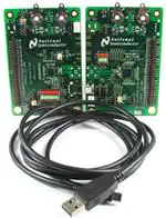
The LV24EVK01 boards uses USB connectors as the serial Channel Link II inputs/outputs. SMA connectors can also be
attached and configured for serial input/output if other types of the cable are desired.
Features
•
•
•
•
•
•
•
•
•
•
•
•
10 – 75 MHz support for 240 Mbps – 1.8 Gbps application payload (280 Mbps to 2.1 Gbps Serial Link)
LVCMOS parallel interface: 24-bit data + 3 low speed control + clock
RGB888 + VS, HS, DE serialized to 1 pair
AC Coupled STP Interconnect up to 10 meters in length
Selectable output VOD, adjustable de-emphasis and receive equalization
Integrated serial terminations
@ Speed link BIST Mode and reporting pin
Optional I2C compatible Serial Control Bus
Power down mode minimizes power dissipation
Randomized, DC-balanced and Scrambled data stream
>8 kV HBM
Backward compatible mode for operation with older generation devices
Applications
•
•
•
Industrial Displays
Machine Vision
Medical Imaging
Ordering Information
PART: LV24EVK01
Demo boards:
Tx: DS92LV2421-EVK
Rx: DS92LV2422-EVK
national.com
© National Semiconductor Corporation 2009
1
Printed in U.S.
�Typical Application Configuration
Quick Start Guide:
DS92LV2421 Tx Board:
1.
Connect 3.3V DC power to the left header pin of JP1 and ground to the right header pin of JP1 of the board. Connect
1.8V DC power to J3 and ground to J4. By default JP2 is configured such that VDDIO = 3.3 V.
2.
Attach the USB cable to the TX board (DS92LV2421) output and to an RX board (DS992LV2422 supplied) input. The
default cable connector on the TX board is P3, which is mounted to the bottom of the evaluation board.
3.
Attach parallel clock and data to the TX board at connector J1. This is typically done with a flat ribbon cable (not
supplied).
4.
Jumpers and switches have been configured at the factory; they should not require any changes for immediate
operation of the board. See text on Configuration Settings and datasheet for more details.
DS92LV2422 Rx Board
5.
Connect 3.3V DC power to the left header pin of JP1 and ground to the right header pin JP1. Connect 1.8V DC
power to J4 and ground to J5.
6.
Attach the USB cable to the RX board (DS92LV2422) input from a TX board (DS92LV2421) output. The default cable
connector on the RX board is J2.
7.
Attach the clock and data outputs to the desired test equipment or other external hardware. This is typically done with
a flat ribbon cable (not supplied).
Jumpers and switches have been configured at the factory; they should not require any changes for immediate operation of
the board. See text on Configuration Settings and datasheet for more details.
national.com
© National Semiconductor Corporation 2009
2
Printed in U.S.
�Tx Board Configuration Settings
Component
Name
Function
Power Connections
J2
5V DC
Optional 5V DC Power Jack.
J3
1.8V DC
1.8V VDD Power.
JP1
3.3V DC
3.3V VDD Power (left header pin) and Ground (right header pin)
J4
VSS
JP2
VDDI
Ground.
Connect to 3.3V for 3.3V input logic levels and I2C interface. Connect to 1.8V for 1.8V
input logic levels and no I2C.
JP18
VDDL
Always connect to 1.8V.
JP23
VDDP
Always connect to 1.8V.
JP24
VDDHS
Always connect to 1.8V.
Input and Output Connections
28 position wall
J1
header
J7 and J8
SMA Connectors
P3
USB Connector
Power Wire in USB
cable through P3
JP25 and JP26
LVCMOS parallel clock and data input.
Channel Link II output.
(When using these connectors, R49 and R50 should be placed with 0Ω resistors, the
traces to the P1 should be cut).
Channel Link II output.
Connect to VSS is recommended.
Control Connections
SW1: 7
RFB
SW1: 6
PDB
SW1: 5
CONFIG0
SW1: 4
CONFIG1
SW1: 3
BISTEN
SW1: 2
VODSEL
SW1: 1
RES2
JP10 and VR4
ID[x]
JP3 and J6
I2C Interface
national.com
© National Semiconductor Corporation 2009
Set to “L” to strobe the input data on the falling clock edge.
Set to “H” to strobe the input data on the rising clock edge.
Set to “L” for the power down mode.
Set to “H” for the normal operation.
Set to “L” to interface with a DS82LV2422 or DS92LV0422.
See datasheet for reverse compatibility mode information
Set to “L” to interface with a DS82LV2422 or DS92LV0422.
See datasheet for reverse compatibility mode information
Set to “H” for the BIST enable mode.
Set to “L” for normal operation.
See datasheet for detail information.
Connect to “L” for low output VOD swing.
Connect to “H” for high output VOD swing.
See datasheet for more information.
Keep RES2 set to “L”
Connect JP19 to VSS to have the default device PHY address (h’EC).
Connect JP19 to VR4; then adjust VR4 value to select desired device PHY address. See
datasheet for detail information.
Connect JP3 if the I2C power is not supplied on J6. Otherwise, leave it unconnected.
3
Printed in U.S.
�Tx Board Bill of Materials
Item Qty Reference
1
2
3
4
2
2
4
2
5
7
6
7
2
2
8
6
9
10
11
5
1
3
12
5
13
5
C1,C15
C16,C2
C3,C4,C8,C9
C5,C6
C7,C14,C20,C23,C
24,C28,
C30
C10,C13
C11,C12
C17,C18,C21,C31,
C32,C33
C19,C25,C26,C27,
C29
C22
JP1,JP3,JP5
JP2,JP10,JP13,JP1
4,JP15
JP4,JP6,JP7,JP8,J
P9
14
2
JP12,JP111
15
1
JP16
16
1
J1
17
18
1
2
J2
J3,J4
19
1
J5
Part
MFR
MFR Part#
Digi-Key Part#
2.2uF
0.1uF
10uF_open
0.1uF
KEMET
KEMET
nichicon
Panasonic
T491B225K020AT
C1206C104K5RACTU
F931C106MBA_open
ECJ-1VB1H104K
399-3714-1-ND
399-1249-1-ND
493-2365-1-ND_open
PCC2398CT-ND
0.1uF
Panasonic
ECJ-1VB1E104K
PCC2277CT-ND
22uF
5pF
nichicon
Panasonic
F931E226MNC
ECJ-ZEC1E050C
493-2391-1-ND
PCC2107CT-ND
22uF
Kemet
T494B226M016AT
399-3835-1-ND
0.01uF
0.1uF_open
2-Pin Header
KEMET
Panasonic
AMP/Tyco
C0603C103K1RACTU
ECJ-0EF1C104Z_open
87220-2
399-3189-1-ND
PCC1731CT-ND_open
A26542-ND
3-Pin Header
2-Pin
Header_open
3-Pin
Header_open
2X10-Pin
Header, open
AMP/Tyco
87224-3
A26545-ND
AMP/Tyco
87220-2_open
A26542-ND_open
AMP/Tyco
87224-3_open
A26545-ND_open
AMP/TYCO
87215-7_open
A26580-ND_open
AMP/TYCO
3-87215-0
A26588-ND
CPU Inc
Johnson
PJ-002A_open
108-0740-001
CP-002A-ND_open
J147-ND
Molex
10-89-7082_open
WM26808-ND_open
HEADER 28x2
CONN JACK
PWR_open
BANANA
2x4 pin
Jumper_open
Molex/Waldo
m Electronics
Corp
22-11-2042
Johnson
Components 142-0701-851_open
20
1
J6
IDC1X4
21
2
J8,J7
22
1
LED1
23
1
LED2
24
1
P1
25
26
1
1
P2
P3
SMA_open
0603_green_L
ED
LITE-ON INC
Lumex
0402_orange_L Opto/Compo
ED
nents Inc
HSD_2X2_ope
n
Rosenberger
mini USB
5pin_open
Hirose
USB A
AMP/Tyco
national.com
© National Semiconductor Corporation 2009
WM2702-ND
J658-ND_open
LTST-C191KGKT_open
160-1446-1-ND_open
SML-LX0402SOCTR_open
67-1879-1-ND_open
D4S20B-40ML5-Y_open
UX60-MB-5ST_open
292303-1
H2959CT-ND_open
A31726-ND
4
Printed in U.S.
�27
1
R1
1.50K
Panasonic
R2,R38,R44,R 0
54,R55
Ohm,0402_open Panasonic
ERJ-2RKF1501X
P1.50KLCT-ND
ERJ2GEJ0R00X_open P0.0JTR-ND_open
28
5
29
29
R3,R4,R5,R6,R
7,R8,R9,R10, 49.9ohm_open
R11,R12,R13,
R14,R15,R16,
R17,R18,R19,
R20,R21,R22,
R23,R24,R25,
R26,R27,R28,
R29,R34,R35
Panasonic
ERJ1GEF49R9C_open P49.9ABCT-ND_open
30
1
R30
49.9ohm_open
R31,R32,R33,
R45,R46,R47, 0 Ohm,0402
R48,R53,R56,
R57
Panasonic
ERJ6ENF49R9V_open P49.9CCT-ND_open
31
10
Panasonic
ERJ-2GEJ0R00X
P0.0JTR-ND
32
1
Panasonic
ERJ3EKF1003V_open
P100KHCT-ND_open
Panasonic
ERJ-3EKF1002V
P10.0KHCT-ND
2
R36
100K_open
R37,R58,R59,
R60,R61,R62, 10K
R63,R64
R40,R39
4.7K
33
8
34
Panasonic
P4.7KGCT-ND
35
2
R42,R41
82.5ohm_open
Panasonic
36
1
R43
100ohm_open
Panasonic
37
38
39
40
2
2
1
1
R49,R50
R52,R51
S1
U1
Panasonic
Panasonic
Grayhill
National
41
2
U2,U3
0 ohm_open
0 ohm
SW DIP-7
DS92LV2421
LM1117IMPADJ/SOT223_op
en
ERJ-3GEYJ472V
ERJ3EKF82R5V_open
ERJ3EKF1000V_open
ERJ1GE0R00C_open
ERJ-1GE0R00C
78B07ST
DS92LV2421
LM1117IMPADJ/NOPB_open
42
1
U4
Oscillator option
43
44
45
46
2
1
1
2
VR2,VR1
VR3
VR4
X2,X1
SVR100_open
SVR20K
SVR100K
TP_0402
LM1117IMPADJ/NOPB_open
ASFLM-BLANKLC_open
3214W-1101E_open
3224W-1-203E
3224W-1-104E
TP_0402
national.com
© National Semiconductor Corporation 2009
National
Abracon
Corporation
Bourns
Bourns
Bourns
P82.5HCT-ND_open
P100HCT-ND_open
P0.0AGCT-ND_open
P0.0AGCT-ND
GH7190-ND
535-10059-5-ND_open
3214W-101ETR-ND_open
3224W-203ECT-ND
3224W-1-104ECT-ND
5
Printed in U.S.
�VDDI
G2
G3
G4
G5
G6
G7
B0
B1
B2
B3
B4
B5
RES2
49
37
38
39
40
41
42
43
44
45
46
47
48
S1
VSS
R57
PDB
VSS
L
H
VSS
DI10
DI11
DI12
DI13
DI14
DI15
DI16
DI17
DI18
DI19
DI20
DI21
C33
22uF
VSS
+
RFB
PDB
CONFG0
CONFG1
BISTEN
VODSEL
RES2
VSS
G2
G3
G4
G5
G6
G7
B0
B1
B2
B3
B4
B5
U1
VDDIc
DS92LV2421
SDA
SCL
PDB
R55
0 Ohm,0402_open
VDDTXc
VSS
C22
1
2
VSS
I2S0
I2S1
VODSEL
DeEmph
VDDTX
PDB
DOUT+
DOUT RES2
VDDHS
RES1
RES0
VDDP
CONFG[1]
BISTEN
R54
0 Ohm,0402_open
RFB
CONFG0
VDDLc
VD D I
R4
R3
R2
R1
R0
R4
R3
R2
R1
R0
VDDI
SW DIP-7
R64
R63
R62
R61
R60
R59
R58
7
6
5
4
3
2
1
8
9
10
11
12
13
14
24
23
22
21
20
19
18
17
16
15
14
13
IDx
VSS
VDDLc
JP10
1
2
3
VSS
VSS
2
VSS
SMA_open
J7
DOUT+_SMA
1
2
3
4
5
0.625"
0.1"
0.1"
1
2
VSS
2
J6
VSS
VR4
0.1uF
VSS
C14
VDDI
VDD_I2C
R38
0 Ohm,0402_open
JP3
X2
C6
C5
X1
0.1uF
C7
VSS
VDD
U4
Oscillator option
PCLK
5
4
3
2
1
Document Number
DS92LV2421 Tx Demo Board
Tuesday , May 18, 2010
Date:
Sheet
2
P3
RES0
RES1
VDDI
JP111
JP12
USB A:
solder
side
(BOTTOM)
P2
VSS
1
2
3
1
2
3
of
4
mini B:
component side
(TOP)
VSS
Rev
2
mini USB 5pin_open
1
2USB A
3
4
VSS
VSS
DS92LV2421 Tx Demo Board - DS92LV2421 Serializer
SDA
SCL
R39
4.7K
0603
VDD
1 JP15
2
3
JP14
DOUT+_USB
DOUT-_USB
Size
A
Title
5pF 5pF
VSS
C12 C11
R40
4.7K
0603
VSS
VDD_I2C
VSS
J8
0402_orange_LED
2
1
DOUT-_SMA
1
LED2
2
2
INT 1
VSS
R44
3
0603_green_LED
JP6
0 Ohm,0402_open
4
2
1
SVR20K
5
VSS
LED1
VR3
RLD 1 JP4 2
1
VSS
CW 3
SMA_open
R1
JP13
VODSEL
1.50K 0402
R45
VSS
JP5
R2
0 Ohm,0402
DeEmph
VDDI
0 Ohm,0402_open
VDDTXc
C5 0.1uF R49 0201 DOUT+_SMA
PDB
1
2 0 ohm_open
DOUT+
+
R51 0201
DOUT+_USB
0 ohm
1
2
RES2
DOUTDOUT-_USB
VDDHSc
C6
R50 0201 DOUT-_SMA
R52 0201
RES1
0.1uF 0 ohm_open
0 ohm
RES0
VSS
X1 1
VDDPc
VSS
VDDI
X2 1
CONFG1
0 Ohm,0402 R33
2
1 JP7
I2S[0]
G1
G1
G0
G0
R7
R7
R6
R6
R5
R5
BISTEN
B6
B7
HS
VS
DE
IDx
0.1uF_open
2
1 JP8
I2S[1]
2
1
36
35
34
33
32
31
30
29
28
27
26
25
DI9
DI8
DI7
DI6
DI5
BISTEN
VDDI
DI4
DI3
DI2
DI1
DI0
B6
B7
HS
VS
DE
+
0201 R34
49.9ohm_open
0201 R35
49.9ohm_open
P12,
DI22
DI23
CI2
CI3
CI1
ID[x]
VDDL
SCL
SDA
CLKIN
TRFB
CONFG[0]
SCL
SDA
PCLK
-
I2S2
2
1 JP9
I2S[2]
10K
10K
10K
10K
10K
10K
10K
0 Ohm,0402
R37
10K
100K_open R36
1
2
3
4
5
6
7
8
9
10
11
12
PCLK
0 Ohm,0402 R31
0 Ohm,0402 R32
1 JP16 2
3
4
5
6
7
8
9
10
11
12
13
14
15
16
17
18
19
20
SVR100K
RED
BLK
VDD
VDDTXc
VDDHS
VDDPc
VDDLc
VDDIc
VSS
1
2
1
CW
3
1
2
3
4
1
VCC Tri-State
4
2
3
P13,
P11,
1
RED 2
3
BLK
1
2
3
GND
OUT
5
6
7
8
6
© National Semiconductor Corporation 2009
1 2 3 4 5 6 7
O
N
national.com
9
VD D
VD D TXc
VD D HSc
VD D Pc
VD D Lc
VD D Ic
VSS
Tx Board Schematics
6
Printed in U.S.
�national.com
© National Semiconductor Corporation 2009
7
Printed in U.S.
VSS
2
4
6
8
10
12
14
16
18
20
22
24
26
28
30
32
34
36
38
40
42
44
46
48
50
52
54
56
R0
R1
R2
R3
R4
R5
R6
R7
G0
G1
G2
G3
G4
G5
G6
G7
B0
B1
B2
B3
B4
B5
B6
B7
HS
VS
DE
PCLK
VSS
Tuesday , May 18, 2010
Date:
Sheet
DS92LV2421 Tx Demo Board - Parallel Input
Document Number
DS92LV2421 Tx Demo Board
Size
A
Title
0201
R3
49.9ohm_open
0201
R4
49.9ohm_open
0201
R5
49.9ohm_open
0201
R6
49.9ohm_open
0201
R7
49.9ohm_open
0201
R8
49.9ohm_open
0201
R9
49.9ohm_open
0201 R10
49.9ohm_open
0201 R11
49.9ohm_open
0201 R12
49.9ohm_open
0201 R13
49.9ohm_open
0201 R14
49.9ohm_open
0201 R15
49.9ohm_open
0201 R16
49.9ohm_open
0201 R17
49.9ohm_open
0201 R18
49.9ohm_open
0201 R19
49.9ohm_open
0201 R20
49.9ohm_open
0201 R21
49.9ohm_open
0201 R22
49.9ohm_open
0201 R23
49.9ohm_open
0201 R24
49.9ohm_open
0201 R25
49.9ohm_open
0201 R26
49.9ohm_open
0201 R27
49.9ohm_open
0201 R28
49.9ohm_open
0201 R29
49.9ohm_open
0805 R30
49.9ohm_open
HEADER 28x2
U SER N OTE:
1) R (0-7),G(0-7),B (0-7),H S,VS,D E, & PC LK are matched length 50 ohm single-ended impedance traces.
2) R 1-R 28 parallel 50 ohm termination option for 50 ohm driving source.
D o not load otherwise.
VSS
1
3
5
7
9
11
13
15
17
19
21
23
25
27
29
31
33
35
37
39
41
43
45
47
49
51
53
55
J1
3
R0
R1
R2
R3
R4
R5
R6
R7
G0
G1
G2
G3
G4
G5
G6
G7
B0
B1
B2
B3
B4
B5
B6
B7
HS
VS
DE
PCLK
of
4
R0
R1
R2
R3
R4
R5
R6
R7
G0
G1
G2
G3
G4
G5
G6
G7
B0
B1
B2
B3
B4
B5
B6
B7
HS
VS
DE
PCLK
Rev
2
50 ohm single-ended impedance traces
�8
Printed in U.S.
1
BANANA
J4
BANANA
C15 +
2.2uF
1
C13 +
22uF
2
1
3
5
7
OPTION AL
5V IN PU T POW ER
C ONN EC TOR
1
2
3
CONN JACK PWR_open
J2
2x4 pin Jumper_open
VSS
J5
2
4
6
8
C4
1
+ C9
VSS
VDD
C8
0.1uF
C16 +
1
2
DIRECT
1.8V INPUT
POWER
CONNECTOR
J3
1
1
2
!!!WARNING!!!
Input power thru J2 OR J3 OR J4
ONLY!!
Input power thru only one connector!!
VSS
1
+
VSS
VSS
+ C3
+
VSS
1.8V
VD D
R41
3
INPUT 82.5oh
2
m_open
Tab/Vout OUTPUT 1
ADJ/GND
4
1
2
10uF_open
2
10uF_open
3.3V
U2
2
JP1
SVR100_open
VSS
VDD3.3V VR1
1
CW 3
R43
100ohm_open
U3
OPTION AL
5V to 3.3V
IN PU T POW ER
R EGULATOR
+
0.1uF
2.2uF
22uF
C2
C1
C10 +
+
OPTIONAL Exte rnal 3.3V input.
OPTIONAL
5V to 1.8V
INPUT POWER
REGULATOR
SVR100_open
VSS
VR2
1
CW 3
1
2
1
2
1
2
2
10uF_open
1
2
10uF_open
LM1117IMP-ADJ/SOT223_open
LM1117IMP-ADJ/SOT223_open
R42
3
INPUT 82.5ohm_open
2
Tab/Vout OUTPUT 1
ADJ/GND
4
2
1
2
VSS
VSS
C28
C24
C23
0.01uF 0.1uF
C26
0.01uF 0.1uF
C25
0.01uF 0.1uF
C27
VSS
R48
0 Ohm,0402
C20
0.01uF 0.1uF
C19
VDDIO=VDD (1.8V)
VDDIO=3.3V (externa l )
JP2
VSS
R47
0 Ohm,0402
C30
0.01uF 0.1uF
C29
+
+
+
+
+
Document Number
DS92LV2421 Tx Demo Board
Tuesday , May 18, 2010
Date:
Sheet
VD D Lc
VD D Pc
VD D H Sc
VD D TXc
VD D Ic
4
of
4
Rev
2
C21
22uF
Place near pin 30 of U1
VDDIc
C18
22uF
Place near pin 22 of U1
VDDTXc
C17
22uF
Place near pin 17 of U1
VDDHSc
C31
22uF
Place near pin 14 of U1
VDDPc
C32
22uF
Place near pin 7 of U1
VDDLc
DS92LV2421 Tx Demo Board - Power and Decoupling
VDD3.3V 1
2
VDDI
3
VDD
VDD
VSS
R46
0 Ohm,0402
VSS
R53
0 Ohm,0402
VSS
R56
0 Ohm,0402
Size
Title
VD DI
VDD3.3V
VDD
VDD
VDD
1
2
1
2
1
2
1
2
1
© National Semiconductor Corporation 2009
2
national.com
�Tx Board Reference Layout
Top Layer
national.com
© National Semiconductor Corporation 2009
Bottom Layer
9
Printed in U.S.
�Rx Board Configuration Settings
Component
Name
Function
Power Connections
J7
5V DC
Optional 5V DC Power Jack.
J4
1.8V DC
1.8V VDD Power.
JP1
3.3V DC
3.3V VDD Power (left header pin) and Ground (right header pin)
J5
VSS
JP2
VDDIO
Input and Output Connections
28 position wall
header
P1
Ground.
Connect to 3.3V for 3.3V input logic levels and I2C interface. Connect to 1.8V for 1.8V
input logic levels and no I2C.
LVCMOS parallel data output.
Channel Link II input. (optional)
(When using these connectors, R53 and R54 should be placed with 0Ω resistors, the
traces to the J1 should be cut).
J3 and J4
SMA Connector
J2
USB Connector
Power Wire in USB
cable through J2
Channel Link II input. (default)
USB Connector
Optional Channel Link II loop through driver output.
JP11 and JP12
P2
Connect to VSS is recommended.
Control Connections
S1: 3
BISTEN
S1: 2
RES0
S1: 1
PDB
JP24 and VR3
ID[x]
J3 and JP23
I2C Interface
Set to “H” for the BIST enable mode.
Set to “L” for normal operation.
See datasheet for detail information.
Keep RES0 set to “L"
Set to “L” for the power down mode.
Set to “H” for the normal operation.
Connect JP19 to VSS to have the default device PHY address (h’EC).
Connect JP19 to VR4; then adjust VR4 value to select desired device PHY address. See
datasheet for detail information.
Connect JP3 if the I2C power is not supplied on J6. Otherwise, leave it unconnected.
Strap Pin Configuration Options
R[1:28], R41, R42
--
Populate with 10k ohm resistor to enable desired strap option. See datasheet for details on
strap options.
Others
LED1
PASS
LED2
LOCK
JP11, JP25, JP26
Other options
national.com
© National Semiconductor Corporation 2009
PASS output. “ON” when PASS is “H”.
See datasheet for detail information.
LOCK output. “ON” when LOCK is “H”.
See datasheet for detail information.
Do not connect
10
Printed in U.S.
�Rx Board Bill of Materials
Part
Item Qty Reference
MFR
______________________________________________
1
2
3
4
5
6
7
8
9
10
11
12
13
Digi-Key Part#
4 C1,C2,C9,C10 10uF_open
6 C3,C7,C21,C2 0.1uF
C4,C8,C22,C2
0.01uF
5 5,C31
4 C5,C6,C15,C1 0.1uF
22uF
2 C11,C14
2.2uF
2 C12,C17
0.1uF
2 C18,C13
C19,C20,C24,
6 C28,C32,C33 22uF
nichicon
Panasonic
F931C106MBA_open
ECJ-1VB1E104K
493-2365-1-ND_open
PCC2277CT-ND
KEMET
Panasonic
nichicon
KEMET
KEMET
C0603C103K1RACTU
ECJ-1VB1H104K
F931E226MNC
T491B225K020AT
C1206C104K5RACTU
399-3189-1-ND
PCC2398CT-ND
493-2391-1-ND
399-3714-1-ND
399-1249-1-ND
Kemet
T494B226M016AT
399-3835-1-ND
C23,C27
C26
C35,C36
JP1,JP16
JP2,JP17,JP1
3 8
Panasonic
Panasonic
Panasonic
AMP/Tyco
ECJ-0EF1C104Z_open PCC1731CT-ND_open
ECJ-0EB0J475M
PCC2475TR-ND
ECJ-ZEC1E050C
PCC2107CT-ND
87220-2
A26542-ND
2
1
2
2
0.1uF_open
4.7µF
5pF
2-Pin Header
3-Pin Header AMP/Tyco
15
16
JP3,JP4,JP5,J 3-Pin
9 P6,JP7,JP10, Header_open AMP/Tyco
JP13,JP14,JP
15
2-Pin
Header_open AMP/Tyco
2 JP8,JP9
3-Pin Header AMP/Tyco
2 JP11,JP12
17
1 JP19
18
1 J1
19
20
21
1 J2
1 J3
2 J4,J5
22
1 J6
23
24
1 J7
2 J9,J8
25
1 J10
26
1 LED1
27
1 LED2
14
MFR Part#
2X10-Pin
Header, open
HSD_2X2_op
en
mini USB
5pin
IDC1X4
BANANA
2x4 pin
Jumper_open
CONN JACK
PWR_open
SMA_open
mini USB
5pin_open
0402_orange
_LED
0603_green_
LED
national.com
© National Semiconductor Corporation 2009
AMP/TYCO
Rosenberger
87224-3
A26545-ND
87224-3_open
A26545-ND_open
87220-2_open
87224-3
A26542-ND_open
A26545-ND
87215-7_open
D4S20B-40ML5Y_open
A26580-ND_open
UX60-MB-5ST
Hirose
Molex/Waldom Electr 22-11-2042
108-0740-001
Johnson
10-89-7082_open
Molex
H2959CT-ND
WM2702-ND
J147-ND
WM26808-ND_open
PJ-002A_open
CPU Inc
Johnson Components142-0701-851_open
CP-002A-ND_open
J658-ND_open
UX60-MB-5ST_open
H2959CT-ND_open
Hirose
Lumex Opto/Compon SML-LX0402SOC-TR 67-1879-1-ND
LITE-ON INC
LTST-C191KGKT
160-1446-1-ND
11
Printed in U.S.
�28
29
30
31
32
33
34
35
36
37
P1
HEADER 28x2
P2
USB A_open
R1,R2,R3,R4,R
10Kohm_open
30 5,R6,R7,R8,
R9,R10,R11,R1
2,R13,R14,
R15,R16,R17,R
18,R19,R20,
R21,R22,R23,R
24,R25,R26,
R27,R28,R41,R
42
R29,R30,R53,R
0 ohm_open
4 54
R31,R37,R38,R
10K
4 39
100K_open
1 R32
0 Ohm,0402_open
1 R33
82.5ohm_open
2 R35,R34
100ohm_open
1 R36
R40,R43,R44,R
0 Ohm,0402
8 45,R46,R47,
R59,R60
AMP/TYCO
AMP/Tyco
3-87215-0
292303-1_open
A26588-ND
A31726-ND_open
Panasonic
ERJ-1GEJ103C_open
P10KAGCT-ND_open
Panasonic
ERJ-1GE0R00C_open
P0.0AGCT-ND_open
Panasonic
Panasonic
Panasonic
Panasonic
Panasonic
ERJ-3EKF1002V
ERJ-3EKF1003V_open
ERJ-2GEJ0R00X_open
ERJ-3EKF82R5V_open
ERJ-3EKF1000V_open
P10.0KHCT-ND
P100KHCT-ND_open
P0.0JTR-ND_open
P82.5HCT-ND_open
P100HCT-ND_open
Panasonic
ERJ-2GEJ0R00X
P0.0JTR-ND
1K Ohm,0402_open Panasonic
ERJ-2GEJ102X_open
P1.0KJCT-ND_open
49.9ohm_open
0 ohm
4.7K
SW DIP-3
DS92LV2422
ERJ-1GEF49R9C_open
ERJ-1GE0R00C
ERJ-3GEYJ472V
78B03ST
DS92LV2422
P49.9ABCT-ND_open
P0.0AGCT-ND
P4.7KGCT-ND
GH7182-ND
LM1117IMPADJ/NOPB_open
3214W-101ETRND_open
3224W-1-503ECT-ND
1
1
38
2
39
40
41
42
43
4
3
2
1
1
R49,R48
R50,R51,R52,R
55
R56,R57,R58
R62,R61
S1
U1
44
2
U2,U3
LM1117IMPADJ/SOT223_open National
LM1117IMPADJ/NOPB_open
45
46
47
2
1
2
VR2,VR1
VR3
X2,X1
SVR100_open
SVR50K
TP_0402
3214W-1-101E_open
3224W-1-503E
TP_0402
national.com
© National Semiconductor Corporation 2009
Panasonic
Panasonic
Panasonic
Grayhill
National
Bourns
Bourns
12
Printed in U.S.
�J2
mini USB 5pin
VD D
JP12
VDDIOc
VDD
1
2
3
4
5
JP11
VDDIO
RIN+_USB
RIN-_USB
VSS
mini B:
component side (BOTTOM)
VSS
5
mini USB 5pin_open 4
3
2
1
J10
1
2
3
4
5
VSS
S1
VSS
L
H
VDDIRc
1
C6
VSS
22uF
C19
+
BISTEN
RES_0
PDB
CMLOUTP
VSS
0.1uF
2
VSS
VDDIRc
VSS
R43
JP16
1
2
IDx
VSS
VDDRc
2
CMLOP
CMLON
VSS
VR3
J3
0.1uF
VSS
C34
VDDIO
VDD_I2C
VSS
2
-
VSS
P2
1
2USB A_open
3
4
VSS
VSS
13
Printed in U.S.
5pF 5pF
VSS
C36 C35
R62
4.7K
0603
VSS
VDD_I2C
SDA
SCL
R61
4.7K
0603
USB A:
solder side
(BOTTOM)
R47
P45
P45
BISTEN
VSS
NC
TESTEN
VDDIR
RIN+
RINCMF
CMLOUTP
CMLOUTN
VDDCMLO
VDDR
ID[x]
VDDPR
VDDSC
PDB
NC
VDDIRc
NC
VDDL
DO8
DO9
DO10
DO11
VDDIO
DO12
DO13
DO14
DO15
DO16
DO17
DO18
NC
DS92LV2422
2 CMLON
0.1uF
0.1uF
2 CMLOP
Wednesday , May 19, 2010
Document Number
DS92LV2422 Rx Demo Board
G4
G5
G6
G7
B0
B1
B2
P16
Sheet
3
of
5
50 ohm single ended impedance trac es
G4
G5
G6
G7
B0
B1
B2
P16
P30
VDDLc P30
G0
G1 G0
G2 G1
G3 G2
G3
VDDIOc
Rev
2
P45 R29 0201 PDB
JP10 VDDIO0 ohm_open
1
OPTION f or UR906-A
2RRFB R30 0201 CMLOUTN
3
0 ohm_open
VSS
30
29
28
27
26
25
24
23
22
21
20
19
18
17
16
DS92LV2422 Rx Demo Board - DS92LV2422 Deserializer
CMLOUTN 1
C16
Date:
Size
A
Title
61
46
47
48
49
50
51
52
53
54
55
56
57
58
59
60
U1
C15
CMLOUTP 1
VSS
LAYOUT NOTE:
Place X1, X2 near
left edge of C1&C2
body 0.1" aw ay.
VSS
X1 1
X2 1
P46
RES_0
R45
0 Ohm,0402
VSS
P46
VDDIRc
X2
C2
C1
X1
1 JP19 2
3
4
5
6
7
8
9
10
11
12
13
14
15
16
17
18
19
20
CMF
CMLOUTP
CMLOUTN
VDDIRc R56 0201
0 ohm VDDRc
CMF
IDx
VDDPRc
VDDSCc
R48
PDB
1K Ohm,0402_open
P60
VSS
P60
0.1"
0.1"
R33
0 Ohm,0402_open
VSS4.7µF
C26
1
CMLOUTN
JP17
1
2
3
R49
1K Ohm,0402_open
2
0.1uF
VDDIRc
C5
1
RIN-_SMA R54 0201 RIN0 ohm_open
SMA_open
J9
VSS
RIN+_SMA R53 0201 RIN+
0 ohm_open
SMA_open
1
2
3
4
5
R57 0201 RIN+
RIN+_USB 0 ohm
RIN-_USB
R58 0201 RIN0 ohm
VSS
0.625"
J8
0.1uF_open
VDDPRc
VSS
VSS
mini B:
VDDIOc
component side (TOP)
6
9
+
VD D PR c
VSS
7
7
8
R39
R38
R37
9
6
8
1
RED 2
3
BLK
1
2
3
RED
BLK
2
C23
SW DIP-3
0.1uF_open
-
C27
1
2
0201 R52
49.9ohm_open
0201 R55
49.9ohm_open
0 Ohm,0402
1
1
2
10K
10K
10K
3
2
1
4
5
6
SVR50K
R31
10K
100K_open R32
+
RED
BLK
VDDRc
VDDSCc
0201 R50
49.9ohm_open
0201 R51
49.9ohm_open
1
CW
3
1
2
3
4
5
0 Ohm,0402
PASS
R0
R1
PASS
R0
R1
R2
P1
SDA
SCL
P1
6
R2
VDDIOc
PCLK
PCLK DE
DE VS
VS HS
HS B7
B7 B6
B6 B5
B5 B4
B4 VDDIOc
VDDSCc
VDDIO
VDDIOc
VDDLc
VDDIRc
VSS
R3
R4
R5
R6
R7
LOCK
P31
R3
R4
R5
R6
R7
LOCK
P31
45
44
43
42
41
40
39
38
37
36
35
34
33
32
31
NC
BISTEN
VDDR
PASS
DO0
DO1
DO2
VDDIO
DO3
DO4
DO5
DO6
DO7
LOCK
NC
NC
SDA
SCL
VDDSC
CLKOUT
CO1
CO3
CO2
DO23
DO22
DO21
DO20
VDDIO
DO19
NC
1
2
3
4
5
6
7
8
9
10
11
12
13
14
15
B3
P15
© National Semiconductor Corporation 2009
B3
P15
national.com
1 2 3
O
N
VD D SC c
VD D IO
VD D IOc
VD D L c
VD D IR c
Rx Board Schematics
�R0
R1
R2
R3
R4
R5
R6
R7
G0
G1
G2
G3
G4
G5
G6
G7
B0
B1
B2
B3
B4
B5
B6
B7
HS
VS
DE
PCLK
VSS
VD D IOc
R0
R1
R2
R3
R4
R5
R6
R7
G0
G1
G2
G3
G4
G5
G6
G7
B0
B1
B2
B3
B4
B5
B6
B7
HS
VS
DE
PCLK
VSS
VDDIOc
PASS
PASS
0201 R42
10Kohm_open
14
Printed in U.S.
JP8
2
STRAP
0402_orange_LED LED1
2
1
"tbd" 1
VDDIOc
LOCK
LOCK
JP9
2
STRAP
0603_green_LED LED2
2
1
"tbd" 1
VDDIOc
Date:
Size
A
Title
P1
2
4
6
8
10
12
14
16
18
20
22
24
26
28
30
32
34
36
38
40
42
44
46
48
50
52
54
56
VDDIOc 1
STRAP 2
VSS 3
Wednesday , May 19, 2010
Document Number
DS92LV2422 Rx Demo Board
Sheet
4
of
5
Rev
2
JP18 U SER N OTE:
JU M PER ST R A P TO VD D IO
TO L OA D STR A P VA LU ES
OTH ER W ISE JU M PER
ST R A P TO VSS.
DS92LV2422 Rx Demo Board - Parallel Output
1
3
5
7
9
11
13
15
17
19
21
23
25
27
29
31
33
35
37
39
41
43
45
47
49
51
53
55
VDDIOc
MAP0
MAP1
SSC0
SSC1
SSC2
SSC3
OSC0
OSC1
OSC2
EQ0
EQ1
EQ2
EQ3
RFB
OSS
RDS
LFM
CF1
CF0
-
0201
R1
10Kohm_open
0201
R2
10Kohm_open
0201
R3
10Kohm_open
0201
R4
10Kohm_open
0201
R5
10Kohm_open
0201
R6
10Kohm_open
0201
R7
10Kohm_open
0201
R8
10Kohm_open
0201
R9
10Kohm_open
0201 R10
10Kohm_open
0201 R11
10Kohm_open
0201 R12
10Kohm_open
0201 R13
10Kohm_open
0201 R14
10Kohm_open
0201 R15
10Kohm_open
0201 R16
10Kohm_open
0201 R17
10Kohm_open
0201 R18
10Kohm_open
0201 R19
10Kohm_open
0201 R20
10Kohm_open
0201 R21
10Kohm_open
0201 R22
10Kohm_open
0201 R23
10Kohm_open
0201 R24
10Kohm_open
0201 R25
10Kohm_open
0201 R26
10Kohm_open
0201 R27
10Kohm_open
0201 R28
10Kohm_open
0201 R41
10Kohm_open
© National Semiconductor Corporation 2009
HEADER 28x2
national.com
�15
Printed in U.S.
1
1
BANANA
J5
1
C17 +
2.2uF
2
1
C14 +
22uF
2
1
3
5
7
OPTION AL
5V IN PU T POW ER
C ONN EC TOR
1
2
3
CONN JACK PWR_open
J7
2x4 pin Jumper_open
VSS
J6
2
4
6
8
VSS
VDD
VDD1.8V
0.1uF
C18 +
1
2
BANANA
+ C10 +
VSS
VD D
VDD3.3V
VSS
+ C1
+
10uF_open
10uF_open
C2
3.3V
10uF_open
10uF_open
C9
1
2
1
2
J4
1
VSS
R34
3
INPUT 82.5ohm_open
2
Tab/Vout OUTPUT 1
ADJ/GND
4
2
1
2
U2
U3
2
JP1
OPTIONAL Exte rnal 3.3V input.
OPTION AL
5V to 3.3V
IN PU T POW ER
R EGULATOR
SVR100_open
VSS
VR1
CW 3
R36 1
100ohm_open
OPTIONAL
5V to 1.8V
INPUT POWER
REGULATOR
SVR100_open
VSS
VR2
1
CW 3
LM1117IMP-ADJ/SOT223_open
LM1117IMP-ADJ/SOT223_open
R35
3
INPUT 82.5ohm_open
2
Tab/Vout OUTPUT 1
ADJ/GND
4
2
1.8V INPUT
POWER
CONNECTOR
0.1uF
C13 +
2.2uF
C12 +
22uF
C11 +
1
2
!!!WARNING!!!
Input power thru J5 OR J4 OR JP3 OR J9
ONLY!!
Input power thru only one connector!!
VSS
1
2
1
2
1
2
VSS
VDD3.3V
VSS
Date:
Size
Title
C30
C21
C3
C7
0.01uF 0.1uF
C8
0.01uF 0.1uF
C4
0.01uF 0.1uF
C22
0.01uF 0.1uF
C31
0.01uF 0.1uF
C29
+
+
+
+
+
Wednesday , May 19, 2010
Document Number
DS92LV2422 Rx Demo Board
Sheet
VD D SC c
VD D Lc
VD D IR c
VD D PR c
VD D IOc
VD D IO
4
of
4
Rev
2
C28
22uF
Place near pin 26 of U1
VDDIOc
VDDIO
C32
22uF
Place near pin 58 of U1
VDDPRc
C24
22uF
Place near pin 51 of U1
VDDIRc
C20
22uF
Place near pin 32 of U1
VDDLc
C33
22uF
Place near pin 6 of U1
VDDSCc
DS92LV2422 Rx Demo Board - Power and Decoupling
VSS
R40
0 Ohm,0402
C25
VDDIO=VDD (1.8V)
VDDIO=3.3V (externa l )
JP2
VSS
R59
0 Ohm,0402
VSS
R46
0 Ohm,0402
VSS
R44
0 Ohm,0402
VSS
R60
0 Ohm,0402
VDDIO
VDD3.3V 1
2
3
VDD
VDD
VDD
VDD
VDD
1
2
1
2
1
2
1
2
1
© National Semiconductor Corporation 2009
2
national.com
�Rx Board Reference Layout
Top Layer
national.com
© National Semiconductor Corporation 2009
Bottom Layer
16
Printed in U.S.
�IMPORTANT NOTICE
Texas Instruments Incorporated and its subsidiaries (TI) reserve the right to make corrections, modifications, enhancements, improvements,
and other changes to its products and services at any time and to discontinue any product or service without notice. Customers should
obtain the latest relevant information before placing orders and should verify that such information is current and complete. All products are
sold subject to TI’s terms and conditions of sale supplied at the time of order acknowledgment.
TI warrants performance of its hardware products to the specifications applicable at the time of sale in accordance with TI’s standard
warranty. Testing and other quality control techniques are used to the extent TI deems necessary to support this warranty. Except where
mandated by government requirements, testing of all parameters of each product is not necessarily performed.
TI assumes no liability for applications assistance or customer product design. Customers are responsible for their products and
applications using TI components. To minimize the risks associated with customer products and applications, customers should provide
adequate design and operating safeguards.
TI does not warrant or represent that any license, either express or implied, is granted under any TI patent right, copyright, mask work right,
or other TI intellectual property right relating to any combination, machine, or process in which TI products or services are used. Information
published by TI regarding third-party products or services does not constitute a license from TI to use such products or services or a
warranty or endorsement thereof. Use of such information may require a license from a third party under the patents or other intellectual
property of the third party, or a license from TI under the patents or other intellectual property of TI.
Reproduction of TI information in TI data books or data sheets is permissible only if reproduction is without alteration and is accompanied
by all associated warranties, conditions, limitations, and notices. Reproduction of this information with alteration is an unfair and deceptive
business practice. TI is not responsible or liable for such altered documentation. Information of third parties may be subject to additional
restrictions.
Resale of TI products or services with statements different from or beyond the parameters stated by TI for that product or service voids all
express and any implied warranties for the associated TI product or service and is an unfair and deceptive business practice. TI is not
responsible or liable for any such statements.
TI products are not authorized for use in safety-critical applications (such as life support) where a failure of the TI product would reasonably
be expected to cause severe personal injury or death, unless officers of the parties have executed an agreement specifically governing
such use. Buyers represent that they have all necessary expertise in the safety and regulatory ramifications of their applications, and
acknowledge and agree that they are solely responsible for all legal, regulatory and safety-related requirements concerning their products
and any use of TI products in such safety-critical applications, notwithstanding any applications-related information or support that may be
provided by TI. Further, Buyers must fully indemnify TI and its representatives against any damages arising out of the use of TI products in
such safety-critical applications.
TI products are neither designed nor intended for use in military/aerospace applications or environments unless the TI products are
specifically designated by TI as military-grade or "enhanced plastic." Only products designated by TI as military-grade meet military
specifications. Buyers acknowledge and agree that any such use of TI products which TI has not designated as military-grade is solely at
the Buyer's risk, and that they are solely responsible for compliance with all legal and regulatory requirements in connection with such use.
TI products are neither designed nor intended for use in automotive applications or environments unless the specific TI products are
designated by TI as compliant with ISO/TS 16949 requirements. Buyers acknowledge and agree that, if they use any non-designated
products in automotive applications, TI will not be responsible for any failure to meet such requirements.
Following are URLs where you can obtain information on other Texas Instruments products and application solutions:
Products
Applications
Audio
www.ti.com/audio
Automotive and Transportation www.ti.com/automotive
Amplifiers
amplifier.ti.com
Communications and Telecom www.ti.com/communications
Data Converters
dataconverter.ti.com
Computers and Peripherals
www.ti.com/computers
DLP® Products
www.dlp.com
Consumer Electronics
www.ti.com/consumer-apps
DSP
dsp.ti.com
Energy and Lighting
www.ti.com/energy
Clocks and Timers
www.ti.com/clocks
Industrial
www.ti.com/industrial
Interface
interface.ti.com
Medical
www.ti.com/medical
Logic
logic.ti.com
Security
www.ti.com/security
Power Mgmt
power.ti.com
Space, Avionics and Defense
www.ti.com/space-avionics-defense
Microcontrollers
microcontroller.ti.com
Video and Imaging
www.ti.com/video
RFID
www.ti-rfid.com
OMAP Mobile Processors
www.ti.com/omap
Wireless Connectivity
www.ti.com/wirelessconnectivity
TI E2E Community Home Page
e2e.ti.com
Mailing Address: Texas Instruments, Post Office Box 655303, Dallas, Texas 75265
Copyright © 2012, Texas Instruments Incorporated
�