Sample &
Buy
Product
Folder
Support &
Community
Tools &
Software
Technical
Documents
MAX202
SLLS576F – JULY 2003 – REVISED SETPEMBER 2016
MAX202 5-V Dual RS-232 Line Driver and Receiver With ±15-kV ESD Protection
1 Features
3 Description
•
The MAX202 device consists of two line drivers, two
line receivers, and a dual charge-pump circuit with
±15-kV ESD protection pin to pin (serial-port
connection pins, including GND). The device meets
the requirements of TIA/EIA-232-F and provides the
electrical interface between an asynchronous
communication controller and the serial-port
connector. The charge pump and four small external
capacitors allow operation from a single 5-V supply.
The device operates at data signaling rates up to
120 kbit/s and a maximum of 30-V/µs driver output
slew rate.
1
•
•
•
•
•
Meets or Exceeds the Requirements of
TIA/EIA-232-F and ITU v.28 Standards
ESD Protection for RS-232 Bus Pins: ±15-kV
Human-Body Model
Operates at 5-V VCC Supply
Operates Up to 120 kbit/s
Two Drivers and Two Receivers
Latch-Up Performance Exceeds 100 mA Per
JESD 78, Class II
2 Applications
•
•
•
•
•
Device Information(1)
Battery-Powered Systems
Notebooks
Laptops
Palmtop PCs
Hand-Held Equipment
PART NUMBER
PACKAGE
BODY SIZE (NOM)
MAX202CD
MAX202ID
SOIC (16)
9.90 mm × 3.91 mm
MAX202CDW
MAX202IDW
SOIC WIDE (16)
10.30 mm × 7.50 mm
MAX202CPW
MAX202IPW
TSSOP (16)
5.00 mm x 4.40 mm
(1) For all available packages, see the orderable addendum at
the end of the data sheet.
Block Diagram
POWER
5V
DIN
2
2
TX
15 kV HBM
120 kb/s
2
ROUT
2
RX
DOUT
RS-232
RIN
RS-232
Copyright © 2016, Texas Instruments Incorporated
1
An IMPORTANT NOTICE at the end of this data sheet addresses availability, warranty, changes, use in safety-critical applications,
intellectual property matters and other important disclaimers. PRODUCTION DATA.
�MAX202
SLLS576F – JULY 2003 – REVISED SETPEMBER 2016
www.ti.com
Table of Contents
1
2
3
4
5
6
7
8
Features ..................................................................
Applications ...........................................................
Description .............................................................
Revision History.....................................................
Pin Configuration and Functions .........................
Specifications.........................................................
1
1
1
2
3
4
6.1
6.2
6.3
6.4
6.5
6.6
6.7
4
4
4
4
5
5
6
Absolute Maximum Ratings ......................................
ESD Ratings..............................................................
Recommended Operating Conditions.......................
Thermal Information ..................................................
Electrical Characteristics...........................................
Switching Characteristics ..........................................
Typical Characteristics .............................................
Parameter Measurement Information .................. 7
Detailed Description .............................................. 8
8.1 Overview ................................................................... 8
8.2 Functional Block Diagram ......................................... 8
8.3 Feature Description................................................... 8
8.4 Device Functional Modes.......................................... 8
9
Application and Implementation ........................ 10
9.1 Application Information............................................ 10
9.2 Typical Application .................................................. 10
10 Power Supply Recommendations ..................... 13
11 Layout................................................................... 13
11.1 Layout Guidelines ................................................ 13
11.2 Layout Example .................................................... 13
12 Device and Documentation Support ................. 14
12.1
12.2
12.3
12.4
12.5
Receiving Notification of Documentation Updates
Community Resources..........................................
Trademarks ...........................................................
Electrostatic Discharge Caution ............................
Glossary ................................................................
14
14
14
14
14
13 Mechanical, Packaging, and Orderable
Information ........................................................... 14
4 Revision History
NOTE: Page numbers for previous revisions may differ from page numbers in the current version.
Changes from Revision E (April 2007) to Revision F
Page
•
Added ESD Ratings table, Feature Description section, Device Functional Modes, Application and Implementation
section, Power Supply Recommendations section, Layout section, Device and Documentation Support section, and
Mechanical, Packaging, and Orderable Information section .................................................................................................. 1
•
Removed the Ordering Information table; see POA at the end of the data sheet ................................................................. 1
•
Changed values in the Thermal Information table to align with JEDEC standards................................................................ 4
2
Submit Documentation Feedback
Copyright © 2003–2016, Texas Instruments Incorporated
Product Folder Links: MAX202
�MAX202
www.ti.com
SLLS576F – JULY 2003 – REVISED SETPEMBER 2016
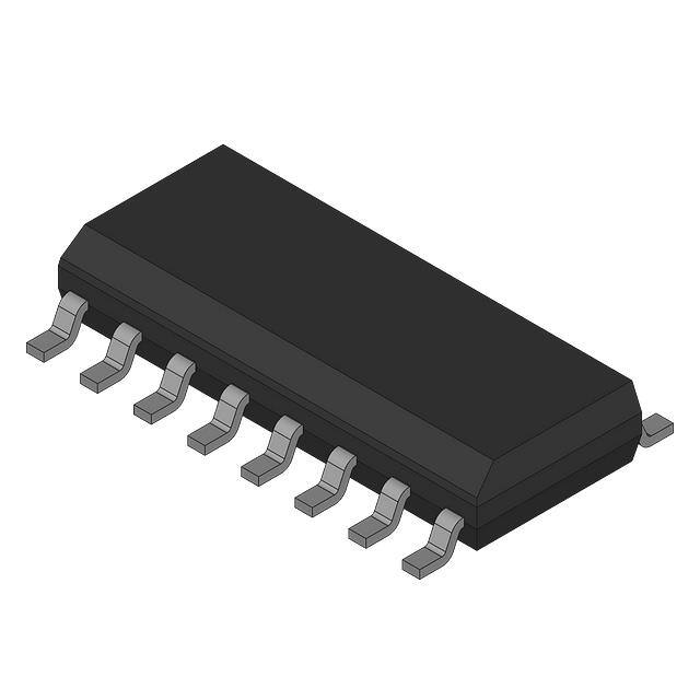
5 Pin Configuration and Functions
D, DW, or PW Package
16-Pin SOIC or TSSOP
Top View
C1+
1
16
VCC
V+
2
15
GND
C1±
3
14
DOUT1
C2+
4
13
RIN1
C2±
5
12
ROUT1
V±
6
11
DIN1
DOUT2
7
10
DIN2
RIN2
8
9
ROUT2
Not to scale
Pin Functions
PIN
NO.
1
NAME
C1+
I/O
DESCRIPTION
—
Positive lead of C1 capacitor
2
V+
O
Positive charge pump output for storage capacitor only
3
C1–
—
Negative lead of C1 capacitor
4
C2+
—
Positive lead of C2 capacitor
5
C2–
—
Negative lead of C2 capacitor
6
V–
O
Negative charge pump output for storage capacitor only
7
DOUT2
O
RS-232 line data output (to remote RS-232 system)
8
RIN2
I
RS-232 line data input (from remote RS-232 system)
9
ROUT2
O
Logic data output (to UART)
10
DIN2
I
Logic data input (from UART)
11
DIN1
I
Logic data input (from UART)
12
ROUT1
O
Logic data output (to UART)
13
RIN1
I
RS-232 line data input (from remote RS-232 system)
14
DOUT1
O
RS-232 line data output (to remote RS-232 system)
15
GND
—
Ground
16
VCC
—
Supply voltage, connect to external 5-V power supply
Submit Documentation Feedback
Copyright © 2003–2016, Texas Instruments Incorporated
Product Folder Links: MAX202
3
�MAX202
SLLS576F – JULY 2003 – REVISED SETPEMBER 2016
www.ti.com
6 Specifications
6.1 Absolute Maximum Ratings
over operating free-air temperature range (unless otherwise noted) (1)
MIN
MAX
UNIT
–0.3
6
V
VCC – 0.3
14
V
–14
0.3
V
–0.3
V+ + 0.3
Supply voltage, VCC (2)
Positive charge pump voltage, V+
(2)
Negative charge pump voltage, V– (2)
Drivers
Input voltage, VI
Receivers
Drivers
Output voltage, VO
V– – 0.3
V+ + 0.3
–0.3
VCC + 0.3
Receivers
Short-circuit duration, DOUT
Storage temperature, Tstg
(2)
V
Continuous
Operating junction temperature, TJ
(1)
V
±30
–65
150
°C
150
°C
Stresses beyond those listed under Absolute Maximum Ratings may cause permanent damage to the device. These are stress ratings
only, which do not imply functional operation of the device at these or any other conditions beyond those indicated under Recommended
Operating Conditions. Exposure to absolute-maximum-rated conditions for extended periods may affect device reliability.
All voltages are with respect to network GND.
6.2 ESD Ratings
VALUE
Electrostatic
discharge
V(ESD)
(1)
(2)
Human-body model (HBM), per ANSI/ESDA/JEDEC JS-001 (1)
Pins 7, 8, 13, and 14
±15000
All other pins
±2000
Charged-device model (CDM), per JEDEC specification JESD22-C101 (2)
UNIT
V
±1500
JEDEC document JEP155 states that 500-V HBM allows safe manufacturing with a standard ESD control process.
JEDEC document JEP157 states that 250-V CDM allows safe manufacturing with a standard ESD control process.
6.3 Recommended Operating Conditions
over operating free-air temperature range (unless otherwise noted (1); see Figure 10)
Supply voltage
VIH
Driver high-level input voltage (DIN)
VIL
Driver low-level input voltage (DIN)
(1)
MAX
5
5.5
MAX202C
Operating free-air temperature
MAX202I
UNIT
V
V
0.8
Receiver input voltage
TA
NOM
4.5
2
Driver input voltage (DIN)
VI
MIN
0
5.5
–30
30
0
70
–40
85
V
V
°C
Test conditions are C1–C4 = 0.1 µF at VCC = 5 V ±0.5 V.
6.4 Thermal Information
MAX202
THERMAL METRIC
(1)
D (SOIC)
DW (SOIC)
PW (TSSOP)
16 PINS
16 PINS
16 PINS
UNIT
RθJA
Junction-to-ambient thermal resistance
76.2
76.8
101
°C/W
RθJC(top)
Junction-to-case (top) thermal resistance
36.8
39.6
36.4
°C/W
RθJB
Junction-to-board thermal resistance
33.9
41.5
45.9
°C/W
ψJT
Junction-to-top characterization parameter
6.7
12.6
2.7
°C/W
ψJB
Junction-to-board characterization parameter
33.6
40.9
45.3
°C/W
(1)
4
For more information about traditional and new thermal metrics, see the Semiconductor and IC Package Thermal Metrics application
report.
Submit Documentation Feedback
Copyright © 2003–2016, Texas Instruments Incorporated
Product Folder Links: MAX202
�MAX202
www.ti.com
SLLS576F – JULY 2003 – REVISED SETPEMBER 2016
6.5 Electrical Characteristics
over recommended ranges of supply voltage and operating free-air temperature (unless otherwise noted; see Figure 10) (1)
PARAMETER
ICC
Supply current
TEST CONDITIONS
MIN
No load, VCC = 5 V
TYP (2)
MAX
8
15
UNIT
mA
DRIVER SECTION
VOH
High-level output voltage
DOUT at RL = 3 kΩ to GND, DIN = GND
5
9
V
VOL
Low-level output voltage
DOUT at RL = 3 kΩ to GND, DIN = VCC
–5
–9
V
IIH
High-level input current
VI = VCC
0
200
IIL
Low-level input current
VI at 0 V
0
–200
µA
IOS (3)
Short-circuit output current
VCC = 5.5 V, VO = 0 V
±10
±60
mA
rO
Output resistance
VCC, V+, and V– = 0 V, VO = ±2 V
300
3.5
µA
Ω
RECEIVER SECTION
VOH
High-level output voltage
IOH = –1 mA
VOL
Low-level output voltage
IOL = 1.6 mA
VIT+
Positive-going input threshold voltage
VCC = 5 V, TA = 25°C
VIT–
Negative-going input threshold voltage
VCC = 5 V, TA = 25°C
Vhys
Input hysteresis (VIT+ – VIT–)
ri
Input resistance
(1)
(2)
(3)
VI = ±3 V to ±25 V
VCC – 0.4
V
1.7
0.4
V
2.4
V
0.8
1.2
0.2
0.5
1
V
V
3
5
7
kΩ
Test conditions are C1–C4 = 0.1 µF at VCC = 5 V ± 0.5 V.
All typical values are at VCC = 5 V, and TA = 25°C.
Short-circuit durations should be controlled to prevent exceeding the device absolute power-dissipation ratings, and not more than one
output should be shorted at a time.
6.6 Switching Characteristics
over recommended ranges of suply voltage and operating free-air temperature (unless otherwise noted; see Figure 10) (1)
PARAMETER
TEST CONDITIONS
MIN
TYP (2)
MAX
UNIT
DRIVER SECTION
Maximum data rate
CL = 50 pF to 1000 pF, RL = 3 kΩ to 7 kΩ
one DOUT switching, see Figure 6
tPLH(D)
Propagation delay time,
low- to high-level output
CL = 2500 pF, RL = 3 kΩ, all drivers loaded,
see Figure 6
2
µs
tPHL(D)
Propagation delay time,
high- to low-level output
CL = 2500 pF, RL = 3 kΩ, all drivers loaded,
see Figure 6
2
µs
tsk(p)
Pulse skew (3)
CL = 150 to 2500 pF, RL = 3 kΩ to 7 kΩ,
see Figure 7
300
ns
SR(tr)
Slew rate, transition region
CL = 50 to 1000 pF, RL = 3 kΩ to 7 kΩ,
VCC = 5 V, see Figure 6
120
3
kbit/s
6
30
V/µs
RECEIVER SECTION (SEE Figure 8)
tPLH(R)
Propagation delay time,
low- to high-level output
CL = 150 pF
0.5
10
µs
tPHL(R)
Propagation delay time,
high- to low-level output
CL = 150 pF
0.5
10
µs
CL = 150 pF
300
tsk(p)
(1)
(2)
(3)
Pulse skew
(3)
ns
Test conditions are C1–C4 = 0.1 µF at VCC = 5 V ± 0.5 V.
All typical values are at VCC = 5 V, and TA = 25°C.
Pulse skew is defined as |tPLH – tPHL| of each channel of the same device.
Submit Documentation Feedback
Copyright © 2003–2016, Texas Instruments Incorporated
Product Folder Links: MAX202
5
�MAX202
SLLS576F – JULY 2003 – REVISED SETPEMBER 2016
www.ti.com
6.7 Typical Characteristics
0.7
0.65
0.6
0.55
0.5
0.45
0.4
0.35
0.3
0.25
0.2
0.15
0.1
0.05
0
5
4.8
ROUT Voltage (V)
ROUT Voltage (V)
at TA = 25°C (unless otherwise noted)
4.6
4.4
4.2
4
3.8
3.6
0
1
2
3
4
5
6
7
ROUT Current (mA)
8
9
10
0
Figure 1. Receiver VOL vs Output Current
2
3
4
5
6
7
ROUT Current (mA)
8
9
10
D002
Figure 2. Receiver VOH vs Output Current
-2.5
-3
-3.5
-4
-4.5
-5
-5.5
-6
-6.5
-7
-7.5
-8
-8.5
-9
-9.5
-10
10
9.5
9
8.5
DOUT Voltage (V)
DOUT Voltage (V)
1
D001
8
7.5
7
6.5
6
5.5
5
4.5
4
0
1
2
3
4
5
6
7
DOUT Current (mA)
8
9
10
0
1
2
3
D003
Figure 3. Driver VOL vs Output Current
4
5
6
7
DOUT Current (mA)
8
9
10
D004
Figure 4. Driver VOH vs Output Current
12
DIN
DOUT
ROUT
9
Waveform (V)
6
3
0
-3
-6
-9
-12
0
2
4
6
8
10
Time (us)
12
14
16
18
D005
Figure 5. Driver and Receiver Loopback Waveforms
6
Submit Documentation Feedback
Copyright © 2003–2016, Texas Instruments Incorporated
Product Folder Links: MAX202
�MAX202
www.ti.com
SLLS576F – JULY 2003 – REVISED SETPEMBER 2016
7 Parameter Measurement Information
3V
Input
Generator
(see Note B)
1.5 V
RS-232
Output
50 W
RL
1.5 V
0V
tPHL (D)
CL
(see Note A)
Output
tPLH (D)
3V
–3 V
TEST CIRCUIT
SR(tf) =
6V
tPHL(D) or tPLH(D)
VOH
3V
–3 V
VOL
VOLTAGE WAVEFORMS
A.
CL includes probe and jig capacitance.
B.
The pulse generator has the following characteristics: PRR = 120 kbit/s, ZO = 50 Ω, 50% duty cycle, tr ≤ 10 ns,
tf ≤ 10 ns.
Figure 6. Driver Slew Rate
3V
Generator
(see Note B)
RS-232
Output
50 W
RL
Input
1.5 V
1.5 V
0V
CL
(see Note A)
tPHL (D)
tPLH (D)
VOH
50%
50%
Output
VOL
TEST CIRCUIT
VOLTAGE WAVEFORMS
A.
CL includes probe and jig capacitance.
B.
The pulse generator has the following characteristics: PRR = 120 kbit/s, ZO = 50 Ω, 50% duty cycle, tr ≤ 10 ns,
tf ≤ 10 ns.
Figure 7. Driver Pulse Skew
Input
Generator
(see Note B)
3V
1.5 V
1.5 V
–3 V
Output
50 W
CL
(see Note A)
tPHL (R)
tPLH (R)
VOH
50%
Output
50%
VOL
TEST CIRCUIT
VOLTAGE WAVEFORMS
A.
CL includes probe and jig capacitance.
B.
The pulse generator has the following characteristics: ZO = 50 Ω, 50% duty cycle, tr ≤ 10 ns, tf ≤ 10 ns.
Figure 8. Receiver Propagation Delay Times
Submit Documentation Feedback
Copyright © 2003–2016, Texas Instruments Incorporated
Product Folder Links: MAX202
7
�MAX202
SLLS576F – JULY 2003 – REVISED SETPEMBER 2016
www.ti.com
8 Detailed Description
8.1 Overview
The MAX202 device is a dual driver and receiver that includes a capacitive voltage generator using four
capacitors to supply TIA/EIA-232-F voltage levels from a single 5-V supply. Each receiver converts TIA/EIA-232F inputs to 5-V TTL/CMOS levels. These receivers have shorted and open fail safe. The receiver can accept up
to ±30-V inputs and decode inputs as low as ±3 V. Each driver converts TTL/CMOS input levels into TIA/EIA232-F levels. Outputs are protected against shorts to ground.
8.2 Functional Block Diagram
POWER
5V
DIN
2
2
TX
15 kV HBM
120 kb/s
2
ROUT
DOUT
RS-232
2
RX
RIN
RS-232
Copyright © 2016, Texas Instruments Incorporated
8.3 Feature Description
8.3.1 Power
The power block increases and inverts the 5-V supply for the RS-232 driver using a charge pump that requires
four 0.1-µF external capacitors.
8.3.2 RS-232 Driver
Two drivers interface standard logic levels to RS-232 levels. The driver inputs do not have internal pullup
resistors. Do not float the driver inputs.
8.3.3 RS-232 Receiver
Two Schmitt trigger receivers interface RS-232 levels to standard logic levels. Each receiver has an internal 5-kΩ
load to ground. An open input results in a high output on ROUT.
8.4 Device Functional Modes
8.4.1 VCC Powered by 5-V
The device is in normal operation when powered by 5 V.
8.4.2 VCC Unpowered
When MAX202 is unpowered, it can be safely connected to an active remote RS-232 device.
8
Submit Documentation Feedback
Copyright © 2003–2016, Texas Instruments Incorporated
Product Folder Links: MAX202
�MAX202
www.ti.com
SLLS576F – JULY 2003 – REVISED SETPEMBER 2016
Device Functional Modes (continued)
8.4.3 Truth Tables
Table 1 and Table 2 list the function for each driver and receiver (respectively).
Table 1. Function Table for
Each Driver (1)
(1)
INPUT
DIN
OUTPUT
DOUT
L
H
H
L
H = high level, L = low level
Table 2. Function Table for
Each Receiver (1)
(1)
INPUT
RIN
OUTPUT
ROUT
L
H
H
L
Open
H
H = high level, L = low level,
Open = input disconnected or
connected driver off
11
14
DIN1
DOUT1
10
7
DIN2
DOUT2
12
13
ROUT1
RIN1
9
8
ROUT2
RIN2
Figure 9. Logic Diagram (Positive Logic)
Submit Documentation Feedback
Copyright © 2003–2016, Texas Instruments Incorporated
Product Folder Links: MAX202
9
�MAX202
SLLS576F – JULY 2003 – REVISED SETPEMBER 2016
www.ti.com
9 Application and Implementation
NOTE
Information in the following applications sections is not part of the TI component
specification, and TI does not warrant its accuracy or completeness. TI’s customers are
responsible for determining suitability of components for their purposes. Customers should
validate and test their design implementation to confirm system functionality.
9.1 Application Information
For proper operation, add capacitors as shown in Figure 10. Pins 9 through 12 connect to UART or general
purpose logic lines. RS-232 lines on pins 7, 8, 13, and 14 connect to a connector or cable.
9.2 Typical Application
1
C1 +
C3 +
0.1 mF,
–
0.1 mF
6.3 V
–
16 V
VCC
C1+
16
+ CBYPASS
– = 0.1 mF,
2
V+
GND
15
14
3
DOUT1
C1–
13
4
C2
0.1 mF,
16 V
C2+
5 kW
+
–
5 C2–
12
C4
0.1 mF,
16 V
RIN1
6
–
11
V–
ROUT1
DIN1
+
DOUT2
RIN2
7
10
8
9
DIN2
ROUT2
5 kW
Copyright © 2016, Texas Instruments Incorporated
A.
C3 can be connected to VCC or GND.
B.
Resistor values shown are nominal.
C.
Nonpolarized ceramic capacitors are acceptable. If polarized tantalum or electrolytic capacitors are used, they must
be connected as shown.
Figure 10. Typical Operating Circuit and Capacitor Values
9.2.1 Design Requirements
•
•
10
VCC minimum is 4.5 V and maximum is 5.5 V.
Maximum recommended bit rate is 120 kbps.
Submit Documentation Feedback
Copyright © 2003–2016, Texas Instruments Incorporated
Product Folder Links: MAX202
�MAX202
www.ti.com
SLLS576F – JULY 2003 – REVISED SETPEMBER 2016
Typical Application (continued)
9.2.2 Detailed Design Procedure
9.2.2.1 Capacitor Selection
The capacitor type used for C1 through C4 is not critical for proper operation. The MAX202 requires 0.1-µF
capacitors. Capacitors up to 10 µF can be used without harm. Ceramic dielectrics are suggested for the 0.1-µF
capacitors. When using the minimum recommended capacitor values, make sure the capacitance value does not
degrade excessively as the operating temperature varies. If in doubt, use capacitors with a larger (for example,
2×) nominal value. The capacitors' effective series resistance (ESR), which usually rises at low temperatures,
influences the amount of ripple on V+ and V–.
Use larger capacitors (up to 10 µF) to reduce the output impedance at V+ and V–.
Bypass VCC to ground with at least 0.1 µF. In applications sensitive to power-supply noise generated by the
charge pumps, decouple VCC to ground with a capacitor the same size as (or larger than) the charge-pump
capacitors (C1 to C4).
9.2.2.2 ESD Protection
MAX202 devices have standard ESD protection structures incorporated on all pins to protect against electrostatic
discharges encountered during assembly and handling. In addition, the RS-232 bus pins (driver outputs and
receiver inputs) of these devices have an extra level of ESD protection. Advanced ESD structures were designed
to successfully protect these bus pins against ESD discharge of ±15-kV when powered down.
9.2.2.3 ESD Test Conditions
Stringent ESD testing is performed by TI based on various conditions and procedures. Please contact TI for a
reliability report that documents test setup, methodology, and results.
9.2.2.4 Human-Body Model (HBM)
The HBM of ESD testing is shown in Figure 11. Figure 12 shows the current waveform that is generated during a
discharge into a low impedance. The model consists of a 100-pF capacitor, charged to the ESD voltage of
concern, and subsequently discharged into the device under test (DUT) through a 1.5-kΩ resistor.
RD
1.5 kW
VHBM
CS
+
-
100 pF
DUT
Figure 11. HBM ESD Test Circuit
Submit Documentation Feedback
Copyright © 2003–2016, Texas Instruments Incorporated
Product Folder Links: MAX202
11
�MAX202
SLLS576F – JULY 2003 – REVISED SETPEMBER 2016
www.ti.com
Typical Application (continued)
1.5
VHBM = 2 kV
DUT = 10-V, 1-W Zener Diode
|
IDUT - A
1.0
0.5
0.0
0
50
100
150
200
Time - ns
Figure 12. Typical HBM Current Waveform
9.2.3 Application Curve
12
DIN
DOUT
ROUT
9
Waveform (V)
6
3
0
-3
-6
-9
-12
0
2
4
6
8
10
Time (us)
12
14
16
18
D006
120 kbit/s, 1-nF load
Figure 13. Driver and Receiver Loopback Signal
12
Submit Documentation Feedback
Copyright © 2003–2016, Texas Instruments Incorporated
Product Folder Links: MAX202
�MAX202
www.ti.com
SLLS576F – JULY 2003 – REVISED SETPEMBER 2016
10 Power Supply Recommendations
The VCC voltage must be connected to the same power source used for logic device connected to DIN and
ROUT pins. VCC must be between 4.5 V and 5.5 V.
11 Layout
11.1 Layout Guidelines
Keep the external capacitor traces short. This is more important on C1 and C2 nodes that have the fastest rise
and fall times. For best ESD performance, make the impedance from MAX202 ground pin to the ground plane of
the circuit board as low as possible. Use wide metal and multiple vias on both sides of ground pin.
11.2 Layout Example
Ground
C3
1 C1+
VCC 16
VCC
PF
C1
2 V+
GND 15
3 C1-
DOUT1 14
4 C2+
RIN1 13
5 C2-
ROUT1 12
Ground
C2
Ground
6 V-
DIN1 11
7 DOUT2
DIN2 10
C4
8 RIN2
ROUT2 9
Figure 14. MAX202 Circuit Board Layout
Submit Documentation Feedback
Copyright © 2003–2016, Texas Instruments Incorporated
Product Folder Links: MAX202
13
�MAX202
SLLS576F – JULY 2003 – REVISED SETPEMBER 2016
www.ti.com
12 Device and Documentation Support
12.1 Receiving Notification of Documentation Updates
To receive notification of documentation updates, navigate to the device product folder on ti.com. In the upper
right corner, click on Alert me to register and receive a weekly digest of any product information that has
changed. For change details, review the revision history included in any revised document.
12.2 Community Resources
The following links connect to TI community resources. Linked contents are provided "AS IS" by the respective
contributors. They do not constitute TI specifications and do not necessarily reflect TI's views; see TI's Terms of
Use.
TI E2E™ Online Community TI's Engineer-to-Engineer (E2E) Community. Created to foster collaboration
among engineers. At e2e.ti.com, you can ask questions, share knowledge, explore ideas and help
solve problems with fellow engineers.
Design Support TI's Design Support Quickly find helpful E2E forums along with design support tools and
contact information for technical support.
12.3 Trademarks
E2E is a trademark of Texas Instruments.
All other trademarks are the property of their respective owners.
12.4 Electrostatic Discharge Caution
These devices have limited built-in ESD protection. The leads should be shorted together or the device placed in conductive foam
during storage or handling to prevent electrostatic damage to the MOS gates.
12.5 Glossary
SLYZ022 — TI Glossary.
This glossary lists and explains terms, acronyms, and definitions.
13 Mechanical, Packaging, and Orderable Information
The following pages include mechanical, packaging, and orderable information. This information is the most
current data available for the designated devices. This data is subject to change without notice and revision of
this document. For browser-based versions of this data sheet, refer to the left-hand navigation.
14
Submit Documentation Feedback
Copyright © 2003–2016, Texas Instruments Incorporated
Product Folder Links: MAX202
�PACKAGE OPTION ADDENDUM
www.ti.com
6-Feb-2020
PACKAGING INFORMATION
Orderable Device
Status
(1)
Package Type Package Pins Package
Drawing
Qty
Eco Plan
Lead/Ball Finish
MSL Peak Temp
(2)
(6)
(3)
Op Temp (°C)
Device Marking
(4/5)
MAX202CD
ACTIVE
SOIC
D
16
40
Green (RoHS
& no Sb/Br)
NIPDAU
Level-1-260C-UNLIM
0 to 70
MAX202C
MAX202CDR
ACTIVE
SOIC
D
16
2500
Green (RoHS
& no Sb/Br)
NIPDAU
Level-1-260C-UNLIM
0 to 70
MAX202C
MAX202CDRE4
ACTIVE
SOIC
D
16
2500
Green (RoHS
& no Sb/Br)
NIPDAU
Level-1-260C-UNLIM
0 to 70
MAX202C
MAX202CDW
ACTIVE
SOIC
DW
16
40
Green (RoHS
& no Sb/Br)
NIPDAU
Level-1-260C-UNLIM
0 to 70
MAX202C
MAX202CDWR
ACTIVE
SOIC
DW
16
2000
Green (RoHS
& no Sb/Br)
NIPDAU
Level-1-260C-UNLIM
0 to 70
MAX202C
MAX202CPW
ACTIVE
TSSOP
PW
16
90
Green (RoHS
& no Sb/Br)
NIPDAU
Level-1-260C-UNLIM
0 to 70
MA202C
MAX202CPWR
ACTIVE
TSSOP
PW
16
2000
Green (RoHS
& no Sb/Br)
NIPDAU
Level-1-260C-UNLIM
0 to 70
MA202C
MAX202ID
ACTIVE
SOIC
D
16
40
Green (RoHS
& no Sb/Br)
NIPDAU
Level-1-260C-UNLIM
-40 to 85
MAX202I
MAX202IDE4
ACTIVE
SOIC
D
16
40
Green (RoHS
& no Sb/Br)
NIPDAU
Level-1-260C-UNLIM
-40 to 85
MAX202I
MAX202IDG4
ACTIVE
SOIC
D
16
40
Green (RoHS
& no Sb/Br)
NIPDAU
Level-1-260C-UNLIM
-40 to 85
MAX202I
MAX202IDR
ACTIVE
SOIC
D
16
2500
Green (RoHS
& no Sb/Br)
NIPDAU
Level-1-260C-UNLIM
-40 to 85
MAX202I
MAX202IDRE4
ACTIVE
SOIC
D
16
2500
Green (RoHS
& no Sb/Br)
NIPDAU
Level-1-260C-UNLIM
-40 to 85
MAX202I
MAX202IDW
ACTIVE
SOIC
DW
16
40
Green (RoHS
& no Sb/Br)
NIPDAU
Level-1-260C-UNLIM
-40 to 85
MAX202I
MAX202IDWR
ACTIVE
SOIC
DW
16
2000
Green (RoHS
& no Sb/Br)
NIPDAU
Level-1-260C-UNLIM
-40 to 85
MAX202I
MAX202IPW
ACTIVE
TSSOP
PW
16
90
Green (RoHS
& no Sb/Br)
NIPDAU
Level-1-260C-UNLIM
-40 to 85
MB202I
MAX202IPWR
ACTIVE
TSSOP
PW
16
2000
Green (RoHS
& no Sb/Br)
NIPDAU
Level-1-260C-UNLIM
-40 to 85
MB202I
MAX202IPWRE4
ACTIVE
TSSOP
PW
16
2000
Green (RoHS
& no Sb/Br)
NIPDAU
Level-1-260C-UNLIM
-40 to 85
MB202I
Addendum-Page 1
Samples
�PACKAGE OPTION ADDENDUM
www.ti.com
6-Feb-2020
(1)
The marketing status values are defined as follows:
ACTIVE: Product device recommended for new designs.
LIFEBUY: TI has announced that the device will be discontinued, and a lifetime-buy period is in effect.
NRND: Not recommended for new designs. Device is in production to support existing customers, but TI does not recommend using this part in a new design.
PREVIEW: Device has been announced but is not in production. Samples may or may not be available.
OBSOLETE: TI has discontinued the production of the device.
(2)
RoHS: TI defines "RoHS" to mean semiconductor products that are compliant with the current EU RoHS requirements for all 10 RoHS substances, including the requirement that RoHS substance
do not exceed 0.1% by weight in homogeneous materials. Where designed to be soldered at high temperatures, "RoHS" products are suitable for use in specified lead-free processes. TI may
reference these types of products as "Pb-Free".
RoHS Exempt: TI defines "RoHS Exempt" to mean products that contain lead but are compliant with EU RoHS pursuant to a specific EU RoHS exemption.
Green: TI defines "Green" to mean the content of Chlorine (Cl) and Bromine (Br) based flame retardants meet JS709B low halogen requirements of