MAX3227
3-V TO 5.5-V SINGLE-CHANNEL RS-232 LINE DRIVER/RECEIVER
WITH ±15-kV ESD PROTECTION
www.ti.com
SLLS673A – AUGUST 2005 – REVISED FEBRUARY 2006
FEATURES
APPLICATIONS
•
•
•
•
•
•
•
•
•
•
•
•
Meets or Exceeds the Requirements of
TIA/EIA-232-F and ITU v.28 Standards
Operates With 3-V to 5.5-V VCC Supply
Operates at Least 1 Mbit/s
Low Standby Current . . . 1 µA Typ
External Capacitors . . . 4 × 0.1 µF
Accepts 5-V Logic Input With 3.3-V Supply
Designed to Be Interchangeable With Maxim™
MAX3227
Latch-Up Performance Exceeds 100 mA Per
JESD 78, Class II
ESD Protection for RS-232 I/O Pins
– ±15 kV – Human-Body Model
– ±8 kV – IEC61000-4-2, Contact Discharge
– ±8 kV – IEC61000-4-2, Air-Gap Discharge
Auto-Powerdown Plus Feature Automatically
Disables Drivers for Power Savings
Packaged in Plastic Shrink Small-Outline
Package
•
•
•
•
Battery-Powered, Hand-Held, and Portable
Equipment
PDAs and Palmtop PCs
Notebooks, Sub-Notebooks, and Laptops
Digital Cameras
Mobile Phones and Wireless Devices
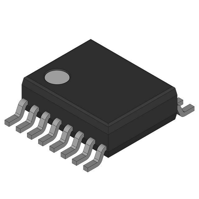
DB PACKAGE
(TOP VIEW)
READY
C1+
V+
C1−
C2+
C2−
V−
RIN
1
16
2
15
3
14
4
13
5
12
6
11
7
10
8
9
FORCEOFF
VCC
GND
DOUT
FORCEON
DIN
INVALID
ROUT
DESCRIPTION/ORDERING INFORMATION
The MAX3227 consists of one line driver, one line receiver, and a dual charge-pump circuit with ±15-kV ESD
protection pin to pin (serial-port connection pins, including GND). The device meets the requirements of
TIA/EIA-232-F and provides the electrical interface between an asynchronous communication controller and the
serial-port connector. The charge pump and four small external capacitors allow operation from a single 3-V to
5.5-V supply. This device operates at data-signaling rates of 1 Mbit/s in normal operating mode and a maximum
of 30-V/µs driver output slew rate. This device also features a logic-level output (READY) that asserts when the
charge pump is regulating and the device is ready to begin transmitting.
The MAX3227 achieves a 1-µA supply current using the auto-powerdown plus feature. This device automatically
enters a low-power powerdown mode when the RS-232 cable is disconnected or the drivers of the connected
peripherals are inactive for more than 30 s. They turn on again when they sense a valid transition at any driver or
receiver input. Auto-powerdown saves power without changes to the existing BIOS or operating system.
The MAX3227C is characterized for operation from 0°C to 70°C. The MAX3227I is characterized for operation
from –40°C to 85°C.
AVAILABLE OPTIONS
PACKAGED DEVICE
TA
SHRINK SMALL OUTLINE
(DB) (1)
0°C to 70°C
MAX3227CDB
–40°C to 85°C
MAX3227IDB
(1)
The DB package is available taped and reeled. Add the suffix R to
device type (e.g., MAX3227CDBR).
Please be aware that an important notice concerning availability, standard warranty, and use in critical applications of Texas
Instruments semiconductor products and disclaimers thereto appears at the end of this data sheet.
All trademarks are the property of their respective owners.
PRODUCTION DATA information is current as of publication date.
Products conform to specifications per the terms of the Texas
Instruments standard warranty. Production processing does not
necessarily include testing of all parameters.
Copyright © 2005–2006, Texas Instruments Incorporated
�MAX3227
3-V TO 5.5-V SINGLE-CHANNEL RS-232 LINE DRIVER/RECEIVER
WITH ±15-kV ESD PROTECTION
www.ti.com
SLLS673A – AUGUST 2005 – REVISED FEBRUARY 2006
FUNCTION TABLE (1)
INPUT CONDITIONS
FORCEON
RECEIVER
OR
DRIVER
FORCEOFF
EDGE
WITHIN
30 s
OUTPUT STATES
VALID
RS-232
LEVEL
PRESENT AT
RECEIVER
DRIVER
RECEIVER
INVALID
READY
OPERATING MODE
Auto-Powerdown Plus Conditions
H
H
NO
NO
Active
Active
L
H
Normal operation,
auto-powerdown plus disabled
H
H
NO
YES
Active
Active
H
H
Normal operation,
auto-powerdown plus disabled
L
H
YES
NO
Active
Active
L
H
Normal operation,
auto-powerdown plus enabled
L
H
YES
YES
Active
Active
H
H
Normal operation,
auto-powerdown plus enabled
L
H
NO
NO
Z
Active
L
L
Powerdown,
auto-powerdown plus enabled
L
H
NO
YES
Z
Active
H
L
Powerdown,
auto-powerdown plus enabled
X
L
X
NO
Z
Active
L
L
Manual powerdown
X
L
X
YES
Z
Active
H
L
Manual powerdown
Auto-Powerdown Conditions
INVALID
INVALID
X
NO
Z
Active
L
L
Powerdown,
auto-powerdown enabled
INVALID
INVALID
X
YES
Active
Active
H
H
Normal operation,
auto-powerdown enabled
(1)
2
H = high level, L = low level, X = irrelevant, Z = high impedance
Submit Documentation Feedback
�MAX3227
3-V TO 5.5-V SINGLE-CHANNEL RS-232 LINE DRIVER/RECEIVER
WITH ±15-kV ESD PROTECTION
www.ti.com
SLLS673A – AUGUST 2005 – REVISED FEBRUARY 2006
TERMINAL FUNCTIONS
TERMINAL
NAME
DESCRIPTION
NO.
C1+
2
Positive terminal of voltage-doubler charge-pump capacitor
C1–
4
Negative terminal of voltage-doubler charge-pump capacitor
C2+
5
Positive terminal of inverting charge-pump capacitor
C2–
6
Negative terminal of inverting charge-pump capacitor
DIN
11
CMOS driver input
DOUT
13
RS-232 driver output
FORCEOFF
16
Force-off input, active low. Drive low to shut down drivers, receivers, and charge pump. This overrides auto-shutdown
and FORCEON (see Function Table).
FORCEON
12
Force-on input, active high. Drive high to override powerdown, keeping drivers and receivers on (FORCEOFF must be
high) (see Function Table).
GND
14
Ground
INVALID
10
Valid signal detector output, active low. A logic high indicates that a valid RS-232 level is present on a receiver input.
READY
1
Ready to transmit output, active high. READY is enabled high when V– goes below –3.5 V and the device is ready to
transmit.
RIN
8
RS-232 receiver input
ROUT
9
CMOS receiver output
V+
3
+2 × VCC generated by the charge pump
V–
7
–2 × VCC generated by the charge pump
VCC
15
3-V to 5.5-V single-supply voltage
LOGIC DIAGRAM (POSITIVE LOGIC)
DIN
FORCEOFF
FORCEON
ROUT
11
13
DOUT
16
12
Auto-Powerdown
Plus
9
10
1
8
Submit Documentation Feedback
INVALID
READY
RIN
3
�MAX3227
3-V TO 5.5-V SINGLE-CHANNEL RS-232 LINE DRIVER/RECEIVER
WITH ±15-kV ESD PROTECTION
www.ti.com
SLLS673A – AUGUST 2005 – REVISED FEBRUARY 2006
Absolute Maximum Ratings (1)
over operating free-air temperature range (unless otherwise noted)
MIN
MAX
VCC
Supply voltage range (2)
–0.3
6
V
V+
Positive output supply voltage range (2)
–0.3
7
V
0.3
–7
V
13
V
V–
Negative output supply voltage
range (2)
V+ – V– Supply voltage difference (2)
VI
Input voltage range
VO
Output voltage range
–0.3
6
Receiver
–25
25
Driver
Receiver (INVALID, READY)
Short-circuit duration
θJA
Driver (FORCEOFF, FORCEON)
–13.2
13.2
–0.3
VCC + 0.3
DOUT to GND
(1)
(2)
(3)
V
V
Unlimited
Package thermal impedance (3)
Lead temperature 1,6 mm (1/16 in) from case for 10 s
Tstg
UNIT
Storage temperature range
–65
82
°C/W
260
°C
150
°C
Stresses beyond those listed under "absolute maximum ratings" may cause permanent damage to the device. These are stress ratings
only, and functional operation of the device at these or any other conditions beyond those indicated under "recommended operating
conditions" is not implied. Exposure to absolute-maximum-rated conditions for extended periods may affect device reliability.
All voltages are with respect to network GND.
The package thermal impedance is calculated in accordance with JESD 51-7.
Recommended Operating Conditions (1)
See Figure 5
MIN NOM MAX
VCC = 3.3 V
Supply voltage
VCC = 5 V
VIH
Driver and control high-level input voltage
DIN, FORCEOFF, FORCEON
VIL
Driver and control low-level input voltage
DIN, FORCEOFF, FORCEON
VI
Receiver input voltage
TA
Operating free-air temperature
(1)
VCC = 3.3 V
VCC = 5 V
MAX3227C
MAX3227I
3
3.3
3.6
4.5
5
5.5
2
5.5
2.4
5.5
UNIT
V
V
0
0.8
V
–25
25
V
0
70
–40
85
°C
Test conditions are C1–C4 = 0.1 µF at VCC = 3.3 V ± 0.3 V; C1 = 0.047 µF, C2–C4 = 0.33 µF at VCC = 5 V ± 0.5 V.
Electrical Characteristics (1)
over recommended ranges of supply voltage and operating free-air temperature (unless otherwise noted) (see Figure 5)
PARAMETER
II
ICC
(1)
(2)
4
Input leakage current
Supply current
(TA = 25°C)
TEST CONDITIONS
FORCEOFF, FORCEON
MIN
TYP (2) MAX
±1
µA
0.3
2
mA
Auto-powerdown plus disabled
No load,
FORCEOFF and FORCEON at VCC
Powered off
No load, FORCEOFF at GND
1
10
Auto-powerdown plus enabled
No load, FORCEOFF at VCC,
FORCEON at GND,
All RIN are open or grounded
1
10
Test conditions are C1–C4 = 0.1 µF at VCC = 3.3 V ± 0.3 V; C1 = 0.047 µF, C2–C4 = 0.33 µF at VCC = 5 V ± 0.5 V.
All typical values are at VCC = 3.3 V or VCC = 5 V, and TA = 25°C.
Submit Documentation Feedback
UNIT
±0.01
µA
�MAX3227
3-V TO 5.5-V SINGLE-CHANNEL RS-232 LINE DRIVER/RECEIVER
WITH ±15-kV ESD PROTECTION
www.ti.com
SLLS673A – AUGUST 2005 – REVISED FEBRUARY 2006
DRIVER SECTION
abc
Electrical Characteristics (1)
over recommended ranges of supply voltage and operating free-air temperature (unless otherwise noted)
(see Figure 1 and Figure 2)
PARAMETER
TEST CONDITIONS
TYP (2) MAX
MIN
High-level output voltage
DOUT at RL = 3 kΩ to GND,
DIN = GND
5
VOL
Low-level output voltage
DOUT at RL = 3 kΩ to GND,
DIN = VCC
–5
IIH
High-level input current
VI = VCC
±0.01
±1
µA
IIL
Low-level input current
VI at GND
±0.01
±1
µA
IOS
Short-circuit output current (3)
ro
Ioff
(1)
(2)
(3)
5.4
UNIT
VOH
V
–5.4
V
VCC = 3.6 V,
VO = 0 V
±35
±60
VCC = 5.5 V,
VO = 0 V
±35
±60
Output resistance
VCC, V+, and V– = 0 V,
VO = ±2 V
Output leakage current
FORCEOFF = GND,
VO = ±12 V,
300
Ω
10M
±25
VCC = 0 to 5.5 V
mA
µA
Test conditions are C1–C4 = 0.1 µF at VCC = 3.3 V ± 0.3 V; C1 = 0.047 µF, C2–C4 = 0.33 µF at VCC = 5 V ± 0.5 V.
All typical values are at VCC = 3.3 V or VCC = 5 V, and TA = 25°C.
Short-circuit durations should be controlled to prevent exceeding the device absolute power dissipation ratings, and not more than one
output should be shorted at a time.
Switching Characteristics (1)
over recommended ranges of supply voltage and operating free-air temperature (unless otherwise noted)
(see Figure 1 and Figure 2)
PARAMETER
Maximum data rate
skew (3)
tsk(p)
Pulse
SR(tr)
Slew rate,
transition region
(1)
(2)
(3)
TEST CONDITIONS
MIN
CL = 1000 pF,
One DIN switching,
RL = 3 kΩ,
See Figure 1
250
CL = 1000 pF,
VCC = 4.5 V,
RL = 3 kΩ,
See Figure 1
One DIN switching,
CL = 250 pF,
VCC = 3 V,
RL = 3 kΩ,
See Figure 1
One DIN switching,
CL = 150 pF to 2500 pF,
RL = 3 kΩ to 7 kΩ,
See Figure 2
VCC = 3.3 V,
CL = 150 pF to 1000 pF,
RL = 3 kΩ to 7 kΩ,
See Figure 1
TYP (2)
MAX
1000
UNIT
kbit/s
1000
25
24
ns
150
V/µs
Test conditions are C1–C4 = 0.1 µF at VCC = 3.3 V ± 0.3 V; C1 = 0.047 µF, C2–C4 = 0.33 µF at VCC = 5 V ± 0.5 V.
All typical values are at VCC = 3.3 V or VCC = 5 V, and TA = 25°C.
Pulse skew is defined as |tPLH – tPHL| of each channel of the same device.
ESD Protection
TERMINAL
NAME
NO.
DOUT
13
TEST CONDITIONS
TYP
UNIT
±15
Human-Body Model
Contact Discharge (IEC61000-4-2)
±8
Air-Gap Discharge (IEC61000-4-2)
±8
Submit Documentation Feedback
kV
5
�MAX3227
3-V TO 5.5-V SINGLE-CHANNEL RS-232 LINE DRIVER/RECEIVER
WITH ±15-kV ESD PROTECTION
www.ti.com
SLLS673A – AUGUST 2005 – REVISED FEBRUARY 2006
RECEIVER SECTION
abc
Electrical Characteristics (1)
over recommended ranges of supply voltage and operating free-air temperature (unless otherwise noted) (see Figure 3)
PARAMETER
VOH
High-level output voltage
IOH = –1 mA
VOL
Low-level output voltage
IOL = 1.6 mA
VIT+
Positive-going input threshold voltage
VIT–
Negative-going input threshold voltage
Vhys
Input hysteresis (VIT+ – VIT–)
Ioff
Output leakage current
ri
Input resistance
MIN
TYP (2)
VCC – 0.6
VCC – 0.1
TEST CONDITIONS
MAX
V
0.4
VCC = 3.3 V
1.5
2.4
VCC = 5 V
1.8
2.4
VCC = 3.3 V
0.6
1.2
VCC = 5 V
0.8
1.5
V
V
V
0.5
VI = ±3 V to ±25 V
UNIT
V
±0.05
±10
µA
5
7
kΩ
3
Test conditions are C1–C4 = 0.1 µF at VCC = 3.3 V ± 0.3 V; C1 = 0.047 µF, C2–C4 = 0.33 µF at VCC = 5 V ± 0.5 V.
All typical values are at VCC = 3.3 V or VCC = 5 V, and TA = 25°C.
(1)
(2)
Switching Characteristics (1)
over recommended ranges of supply voltage and operating free-air temperature (unless otherwise noted)
PARAMETER
TEST CONDITIONS
TYP (2)
UNIT
tPLH
Propagation delay time, low- to high-level output
CL = 150 pF, See Figure 3
150
ns
tPHL
Propagation delay time, high- to low-level output
CL = 150 pF, See Figure 3
150
ns
tsk(p)
Pulse skew (3)
See Figure 3
50
ns
TYP
UNIT
(1)
(2)
(3)
Test conditions are C1–C4 = 0.1 µF at VCC = 3.3 V ± 0.3 V; C1 = 0.047 µF, C2–C4 = 0.33 µF at VCC = 5 V ± 0.5 V.
All typical values are at VCC = 3.3 V or VCC = 5 V, and TA = 25°C.
Pulse skew is defined as |tPLH – tPHL| of each channel of the same device.
ESD Protection
TERMINAL
NAME
NO.
RIN
8
TEST CONDITIONS
±15
Human-Body Model
6
Contact Discharge (IEC61000-4-2)
±8
Air-Gap Discharge (IEC61000-4-2)
±15
Submit Documentation Feedback
kV
�MAX3227
3-V TO 5.5-V SINGLE-CHANNEL RS-232 LINE DRIVER/RECEIVER
WITH ±15-kV ESD PROTECTION
www.ti.com
SLLS673A – AUGUST 2005 – REVISED FEBRUARY 2006
AUTO-POWERDOWN SECTION
xxx
Electrical Characteristics
over recommended ranges of supply voltage and operating free-air temperature (unless otherwise noted) (see Figure 4)
PARAMETER
TEST CONDITIONS
MIN
VT+(valid)
Receiver input threshold
for INVALID high-level output voltage
FORCEON = GND, FORCEOFF = VCC
VT–(valid)
Receiver input threshold
for INVALID high-level output voltage
FORCEON = GND, FORCEOFF = VCC
–2.7
VT(invalid)
Receiver input threshold
for INVALID low-level output voltage
FORCEON = GND, FORCEOFF = VCC
–0.3
VOH
INVALID, READY output voltage high IOH = –1 mA, FORCEON = GND, FORCEOFF = VCC
VOL
INVALID, READY output voltage low
MAX
UNIT
2.7
V
V
0.3
VCC – 0.6
V
V
IOL = 1.6 mA, FORCEON = GND, FORCEOFF = VCC
0.4
V
Switching Characteristics
over recommended ranges of supply voltage and operating free-air temperature (unless otherwise noted) (see Figure 4)
MIN TYP (1) MAX
PARAMETER
UNIT
tINVH
Propagation delay time, low- to high-level output
1
µs
tINVL
Propagation delay time, high- to low-level output
30
µs
tWU
Supply enable time
100
µs
tAUTOPRDN
Driver or receiver edge to driver's shutdown
(1)
VCC = 5 V
15
30
60
s
All typical values are at VCC = 3.3 V or VCC = 5 V, and TA = 25°C.
Submit Documentation Feedback
7
�MAX3227
3-V TO 5.5-V SINGLE-CHANNEL RS-232 LINE DRIVER/RECEIVER
WITH ±15-kV ESD PROTECTION
www.ti.com
SLLS673A – AUGUST 2005 – REVISED FEBRUARY 2006
PARAMETER MEASUREMENT INFORMATION
3V
Generator
(see Note B)
Input
RS-232
Output
50 Ω
RL
3V
3V
Output
SR(tr) �
tTLH
tTHL
CL
(see Note A)
3V
FORCEOFF
TEST CIRCUIT
0V
−3 V
−3 V
6V
t THL or tTLH
VOH
VOL
VOLTAGE WAVEFORMS
NOTES: A. CL includes probe and jig capacitance.
B. The pulse generator has the following characteristics: PRR = 250 kbit/s, ZO = 50 Ω, 50% duty cycle, tr ≤ 10 ns, tf ≤ 10 ns.
Figure 1. Driver Slew Rate
3V
Generator
(see Note B)
RS-232
Output
50 Ω
RL
Input
1.5 V
1.5 V
0V
CL
(see Note A)
tPHL
tPLH
VOH
3V
FORCEOFF
50%
50%
Output
VOL
TEST CIRCUIT
VOLTAGE WAVEFORMS
NOTES: A. CL includes probe and jig capacitance.
B. The pulse generator has the following characteristics: PRR = 250 kbit/s, ZO = 50 Ω, 50% duty cycle, tr ≤ 10 ns, tf ≤ 10 ns.
Figure 2. Driver Pulse Skew
3 V or 0 V
FORCEON
3V
Input
1.5 V
1.5 V
−3 V
Output
Generator
(see Note B)
tPHL
50 Ω
3V
FORCEOFF
tPLH
CL
(see Note A)
VOH
50%
Output
50%
VOL
TEST CIRCUIT
VOLTAGE WAVEFORMS
NOTES: A. CL includes probe and jig capacitance.
B. The pulse generator has the following characteristics: ZO = 50 Ω, 50% duty cycle, tr ≤ 10 ns, tf ≤ 10 ns.
Figure 3. Receiver Propagation Delay Times
8
Submit Documentation Feedback
�MAX3227
3-V TO 5.5-V SINGLE-CHANNEL RS-232 LINE DRIVER/RECEIVER
WITH ±15-kV ESD PROTECTION
www.ti.com
SLLS673A – AUGUST 2005 – REVISED FEBRUARY 2006
PARAMETER MEASUREMENT INFORMATION (continued)
Receiver
Inputs
}
Invalid
Region
Transmitter
Inputs
Transmitter
Outputs
INVALID VCC
tINVL
Output
0
tINVH
tWU
tWU
VCC
Output
0
V+
VCC
0
V−
VOLTAGE WAVEFORMS
�����������
�����������
�����������
�����������
�����������
�����������
Valid RS-232 Level, INVALID High
ROUT
Generator
(see Note B)
2.7 V
50 Ω
Indeterminate
0.3 V
0V
If Signal Remains Within This Region
for More Than 30 µs, INVALID Is Low†
−0.3 V
Auto-Powerdown
Plus
Indeterminate
INVALID
−2.7 V
CL = 30 pF
(see Note A)
Valid RS-232 Level, INVALID High
†
DIN
DOUT
Auto-powerdown disables drivers and reduces supply
current to 1 µA.
TEST CIRCUIT
Figure 4. INVALID Propagation Delay Times and Driver Enabling Time
Submit Documentation Feedback
9
�MAX3227
3-V TO 5.5-V SINGLE-CHANNEL RS-232 LINE DRIVER/RECEIVER
WITH ±15-kV ESD PROTECTION
www.ti.com
SLLS673A – AUGUST 2005 – REVISED FEBRUARY 2006
APPLICATION INFORMATION
READY
16
1
2
VCC
C1+
15
+
3
C1
+
+
−
−
AutoPowerdown
Plus
V+
C3†
4
GND
−
14
13
6
C2−
7
RIN
12
C2
11
V−
10
C4
+
DOUT
C2+
+
−
CBYPASS = 0.1 µF
C1−
5
−
FORCEOFF
8
9
FORCEON
DIN
INVALID
ROUT
5 kΩ
†
C3 can be connected to VCC or GND.
NOTES: A. Resistor values shown are nominal.
B. Nonpolarized ceramic capacitors are acceptable. If polarized tantalum or electrolytic capacitors are used, they should be
connected as shown.
VCC vs CAPACITOR VALUES
VCC
C1
C2, C3, and C4
3.3 V ± 0.3 V
5 V ± 0.5 V
3 V to 5.5 V
0.1 µF
0.047 µF
0.1 µF
0.1 µF
0.33 µF
0.47 µF
Figure 5. Typical Operating Circuit and Capacitor Values
10
Submit Documentation Feedback
�PACKAGE OPTION ADDENDUM
www.ti.com
13-Aug-2021
PACKAGING INFORMATION
Orderable Device
Status
(1)
Package Type Package Pins Package
Drawing
Qty
Eco Plan
(2)
Lead finish/
Ball material
MSL Peak Temp
Op Temp (°C)
Device Marking
(3)
(4/5)
(6)
MAX3227CDB
ACTIVE
SSOP
DB
16
80
RoHS & Green
NIPDAU
Level-1-260C-UNLIM
0 to 70
MP227C
MAX3227CDBG4
ACTIVE
SSOP
DB
16
80
RoHS & Green
NIPDAU
Level-1-260C-UNLIM
0 to 70
MP227C
MAX3227CDBR
ACTIVE
SSOP
DB
16
2000
RoHS & Green
NIPDAU
Level-1-260C-UNLIM
0 to 70
MP227C
MAX3227IDB
ACTIVE
SSOP
DB
16
80
RoHS & Green
NIPDAU
Level-1-260C-UNLIM
-40 to 85
MP227I
MAX3227IDBR
ACTIVE
SSOP
DB
16
2000
RoHS & Green
NIPDAU
Level-1-260C-UNLIM
-40 to 85
MP227I
(1)
The marketing status values are defined as follows:
ACTIVE: Product device recommended for new designs.
LIFEBUY: TI has announced that the device will be discontinued, and a lifetime-buy period is in effect.
NRND: Not recommended for new designs. Device is in production to support existing customers, but TI does not recommend using this part in a new design.
PREVIEW: Device has been announced but is not in production. Samples may or may not be available.
OBSOLETE: TI has discontinued the production of the device.
(2)
RoHS: TI defines "RoHS" to mean semiconductor products that are compliant with the current EU RoHS requirements for all 10 RoHS substances, including the requirement that RoHS substance
do not exceed 0.1% by weight in homogeneous materials. Where designed to be soldered at high temperatures, "RoHS" products are suitable for use in specified lead-free processes. TI may
reference these types of products as "Pb-Free".
RoHS Exempt: TI defines "RoHS Exempt" to mean products that contain lead but are compliant with EU RoHS pursuant to a specific EU RoHS exemption.
Green: TI defines "Green" to mean the content of Chlorine (Cl) and Bromine (Br) based flame retardants meet JS709B low halogen requirements of