�������
�
��
����
� ���W ���� �
���� �� ���
www.ti.com
SLLS642 − JANUARY 2005
Description
The MAX4597 is a single-pole single-throw (SPST)
analog switch that is designed to operate from 2 V to
5.5 V. This device can handle both digital and analog
signals, and signals up to V+ can be transmitted in either
direction.
Applications
D Sample-and-Hold Circuits
Features
D Low ON-State Resistance (10 W)
D ON-State Resistance Flatness (1.5 W)
D Control Inputs Are 5.5-V Tolerant
D Low Charge Injection (5 pC Max)
D 300-MHz −3-dB Bandwidth at 255C
D Low Total Harmonic Distortion (THD) (0.05%)
D 2-V to 5.5-V Single-Supply Operation
D Specified at 5-V and 3.3-V Nodes
D −83-dB OFF Isolation at 1 MHz
D Latch-Up Performance Exceeds 100 mA Per
D
D
D Battery-Powered Equipment
(Cellular Phones, PDAs)
D Audio and Video Signal Routing
JESD 78, Class II
0.5-nA Max OFF Leakage
ESD Performance Tested Per JESD 22
− 2000-V Human-Body Model
(A114-B, Class II)
− 1000-V Charged-Device Model (C101)
TTL/CMOS-Logic Compatible
D Communication Circuits
D
D PCMCIA Cards
Summary of Characteristics
V+ = 5 V, TA = 25°C
Single Pole
Single Throw
(SPST)
Configuration
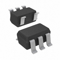
SOT-23 OR SC-70 PACKAGE
(TOP VIEW)
Number of channels
IN 1
5
V+
COM 2
4
GND 3
1
ON-state resistance (ron)
10 Ω
ON-state resistance flatness (ron(flat))
1.5 Ω
Turn-on/turn-off time (tON/tOFF)
NC
35 ns/40 ns
Charge injection (QC)
5 pC
Bandwidth (BW)
300 MHz
OFF isolation (OISO)
FUNCTION TABLE
−83 dB at 1 MHz
Total harmonic distortion (THD)
IN
NC TO COM,
COM TO NC
L
ON
Power-supply current (I+)
H
OFF
Package option
0.05%
±0.05 nA
Leakage current(ICOM(OFF)/INC(OFF))
1 µA
5-pin SOT-23 or SC-70
ORDERING INFORMATION
TA
−40°C to 85°C
PACKAGE(1)
ORDERABLE PART NUMBER
TOP-SIDE MARKING(2)
SOT (SOT-23) − DBV
Tape and reel
MAX4597DBVR
6SD_
SOT (SC−70) − DCK
Tape and reel
MAX4597DCKR
SD_
(1) Package drawings, standard packing quantities, thermal data, symbolization, and PCB design guidelines are available at www.ti.com/sc/package.
(2) DBV/DCK: The actual top-side marking has one additional character that designates the assembly/test site.
Please be aware that an important notice concerning availability, standard warranty, and use in critical applications of Texas Instruments
semiconductor products and disclaimers thereto appears at the end of this data sheet.
������� �
���� ������!"��� �# $%��&�" !# �� '%()�$!"��� *!"&+
���*%$"# $������ "� #'&$���$!"���# '&� ",& "&��# �� �&-!# �#"�%�&�"#
#"!�*!�* .!��!�"/+ ���*%$"��� '��$&##��0 *�&# ��" �&$&##!��)/ ��$)%*&
"&#"��0 �� !)) '!�!�&"&�#+
Copyright 2005, Texas Instruments Incorporated
��������
�
��
����
� ���W ���� �
���� �� ���
www.ti.com
SLLS642 − JANUARY 2005
Pin Configurations
Available in Other Pin Configurations
IN 1
5
V+
4
NC
COM
1
NO
2
GND
3
5
V+
4
IN
COM 2
GND 3
MAX4597
MAX4594
COM
1
NC
2
GND
3
5
V+
IN 1
5
V+
4
NO
COM 2
4
IN
MAX4595
GND 3
MAX4596
Absolute Minimum and Maximum Ratings(1)(2)
over operating free-air temperature range (unless otherwise noted)
V+
VNC
VCOM
IK
INC
ICOM
VI
MIN
MAX
Supply voltage range(3)
−0.3
6
UNIT
V
Analog voltage range(3)(4)
−0.3
V+ + 0.3
V
Analog port diode current
VNC, VCOM < 0
−50
On-state switch current
VNC, VCOM = 0 to V+
−20
20
mA
−0.3
6
V
Digital input voltage range(3)(4)
IIK
I+
Digital input clamp current
IGND
Continuous current through GND
θJA
Package thermal impedance(5)
VI < 0
mA
−50
Continuous current through V+
mA
100
−100
mA
mA
DBV package
206
DCK package
252
°C/W
Tstg
Storage temperature range
−65
150
°C
(1) Stresses above these ratings may cause permanent damage. Exposure to absolute maximum conditions for extended periods may degrade
device reliability. These are stress ratings only, and functional operation of the device at these or any other conditions beyond those specified
is not implied.
(2) The algebraic convention, whereby the most negative value is a minimum and the most positive value is a maximum
(3) All voltages are with respect to ground, unless otherwise specified.
(4) The input and output voltage ratings may be exceeded if the input and output clamp-current ratings are observed.
(5) The package thermal impedance is calculated in accordance with JESD 51-7.
2
��������
�
��
����
� ���W ���� �
���� �� ���
www.ti.com
SLLS642 − JANUARY 2005
Electrical Characteristics for 5-V Supply(1)
V+ = 4.5 V to 5.5 V, TA = −40°C to 85°C (unless otherwise noted)
PARAMETER
TEST CONDITIONS
SYMBOL
TA
V+
MIN
TYP
MAX
UNIT
Analog Switch
Analog signal
range
VCOM,
VNC
0
VNC = 3.5 V,
ICOM = 10 mA,
Switch ON,
See Figure 13
25°C
VNC = 1.5 V, 2.5 V, 3.5 V,
ICOM = 10 mA,
Switch ON,
See Figure 13
25°C
ron(flat)
NC
OFF leakage
current
VNC = 1 V, VCOM = 4.5 V,
or
VNC = 4.5 V, VCOM = 1 V,
Switch OFF,
See Figure 14
25°C
INC(OFF)
COM
OFF leakage
current
VCOM = 1 V, VNC = 4.5 V,
or
VCOM = 4.5 V, VNC = 1 V,
Switch OFF,
See Figure 14
25°C
ICOM(OFF)
INC(ON)
VNC = 1 V, VCOM = 1 V,
or
VNC = 4.5 V, VCOM = 4.5 V,
or
VNC = 1 V, 4.5 V, VCOM = Open,
Switch ON,
See Figure 15
VCOM = 1 V, VNC = 1 V,
or
VCOM = 4.5 V, VNC = 4.5 V,
or
VCOM = 1 V, 4.5 V, VNC = Open,
Switch ON,
See Figure 15
ON-state
resistance
ron
ON-state
resistance
flatness
NC
ON leakage
current
COM
ON leakage
current
ICOM(ON)
Full
V+
6.5
4.5 V
10
12
0.5
2
−0.5
0.01
nA
−5
−0.5
5
0.01
0.5
5.5 V
Full
nA
−5
25°C
Ω
0.5
5.5 V
Full
Ω
1.5
4.5 V
Full
V
−1
5
0.01
1
5.5 V
nA
Full
−10
25°C
−1
10
0.01
1
5.5 V
nA
Full
−10
10
Full
2.4
5.5
V
Full
0
0.8
V
25°C
−1
Digital Control Input (IN)
Input logic high
Input logic low
Input leakage
current
VIH
VIL
IIH, IIL
VI = 5.5 V or 0
Full
5.5 V
−1
0.03
1
1
µA
A
(1) The algebraic convention, whereby the most negative value is a minimum and the most positive value is a maximum
3
��������
�
��
����
� ���W ���� �
���� �� ���
www.ti.com
SLLS642 − JANUARY 2005
Electrical Characteristics for 5-V Supply(1) (continued)
V+ = 4.5 V to 5.5 V, TA = −40°C to 85°C (unless otherwise noted)
PARAMETER
TEST CONDITIONS
SYMBOL
TA
V+
MIN
TYP
MAX
20
35
UNIT
Dynamic
Turn-on time
VNC = 3 V,
RL = 300 Ω,
CL = 35 pF,
See Figure 17
25°C
5V
tON
Full
4.5 V to 5.5 V
Turn-off time
VNC = 3 V,
RL = 300 Ω,
CL = 35 pF,
See Figure 17
25°C
5V
tOFF
Full
4.5 V to 5.5 V
CL = 1 nF,
See Figure 20
25°C
5V
2
Switch OFF,
See Figure 16
25°C
5V
8
pF
45
25
ns
40
50
ns
Charge injection
QC
NC
OFF capacitance
CNC(OFF)
VGEN = 0,
RGEN = 0,
VNC = 0,
f = 1 MHz,
COM
OFF capacitance
CCOM(OFF)
VCOM = 0,
f = 1 MHz,
Switch OFF,
See Figure 16
25°C
5V
8
pF
NC
ON capacitance
CNC(ON))
VNC = 0,
f = 1 MHz,
Switch ON,
See Figure 16
25°C
5V
20
pF
COM
ON capacitance
CCOM(ON)
VCOM = 0,
f = 1 MHz,
Switch ON,
See Figure 16
25°C
5V
20
pF
CI
VI = V+ or GND,
See Figure 16
25°C
5V
3
pF
BW
RL = 50 Ω,
Signal = 0 dBm,
Switch ON,
See Figure 18
25°C
5V
300
MHz
Digital input
capacitance
Bandwidth
5
pC
OFF isolation
OISO
RL = 50 Ω, f = 10 MHz,
VNC = 1 VRMS,
Switch OFF,
See Figure 19
25°C
5V
−83
dB
Total harmonic
distortion
THD
RL = 600 Ω, CL = 50 pF,
VSOURCE = 5 Vp-p,
f = 20 Hz to 20 kHz,
See Figure 21
25°C
5V
0.05
%
Supply
Positive supply
I+
VI = V+ or GND,
Switch ON or OFF
Full
5.5 V
current
(1) The algebraic convention, whereby the most negative value is a minimum and the most positive value is a maximum
4
1
µA
��������
�
��
����
� ���W ���� �
���� �� ���
www.ti.com
SLLS642 − JANUARY 2005
Electrical Characteristics for 3-V Supply(1)
V+ = 2.7 V to 3.6 V, TA = −40°C to 85°C (unless otherwise noted)
PARAMETER
TEST CONDITIONS
SYMBOL
TA
V+
MIN
TYP
MAX
UNIT
Analog Switch
Analog signal
range
ON-state
resistance
VCOM,
VNC
ron
0
VNC = 1.5 V,
ICOM = 10 mA,
Switch ON,
See Figure 13
25°C
Full
V+
10
2.7 V
20
25
V
Ω
Digital Control Input (IN)
Input logic high
Input logic low
VIH
VIL
Full
2
5.5
V
Full
0
0.8
V
Input leakage
current
IIH, IIL
VI = V+ or 0
Turn-on time
VCOM = 2 V,
RL = 300 Ω,
CL = 35 pF,
See Figure 17
25°C
3V
tON
Full
2.7 V to 3.6 V
Turn-off time
VCOM = 2 V,
RL = 300 Ω,
CL = 35 pF,
See Figure 17
25°C
3V
tOFF
Full
2.7 V to 3.6 V
VNC = 0,
CL = 1 nF,
See Figure 20
25°C
3V
25°C
Full
−1
3.6 V
0.03
−1
1
1
µA
A
Dynamic
Charge injection
QC
25
45
55
30
50
60
2
ns
ns
4
pC
1
µA
Supply
Positive supply
I+
VI = V+ or GND,
Switch ON or OFF
Full
3.6 V
current
(1) The algebraic convention, whereby the most negative value is a minimum and the most positive value is a maximum
5
��������
�
��
����
� ���W ���� �
���� �� ���
www.ti.com
SLLS642 − JANUARY 2005
TYPICAL PERFORMANCE
10
8
TA = 25_C
8
6
855C
255C
6
ron (W)
ron (Ω)
V+ = 3 V
4
4
–405C
V+ = 5 V
2
2
0
0
0
1
2
3
4
5
0
1
2
VCOM (V)
1.0
–405C
ICOM(ON)/INO(ON)
0.8
Leakage Current (nA)
8
ron (W)
5
Figure 2. ron vs VCOM (V+ = 5 V)
10
6
4
255C
855C
2
0.6
INO(OFF)/ICOM(OFF)
0.4
0.2
0.0
0
0
1
2
3
VCOM (V)
−40°C
25°C
TA (°C)
85°C
Figure 4. Leakage Current vs Temperature
(V+ = 5 V)
Figure 3. ron vs VCOM (V+ = 3 V)
20
2
18
1
tON
tOFF
16
0
tON/tOFF (ns)
Charge Injection (pC)
4
VCOM (V)
Figure 1. ron vs VCOM
V+ = 3 V
−1
V+ = 5 V
−2
−3
14
12
10
8
6
−4
0
1
2
3
4
Bias Voltage (V)
Figure 5. Charge-Injection (QC) vs VCOM
6
3
5
0
1
2
3
4
5
6
V+ (V)
Figure 6. tON and tOFF vs Supply Voltage
��������
�
��
����
� ���W ���� �
���� �� ���
www.ti.com
SLLS642 − JANUARY 2005
TYPICAL PERFORMANCE
12
Logic Level Threshold (nA)
3
tON/tOFF (ns)
11
10
9
tON
8
7
tOFF
6
−40°C
25°C
VIH
2
1
VIL
0
0
85°C
1
2
TA (5C)
Figure 7. tON and tOFF vs Temperature (V+ = 5 V)
3
V+ (V)
4
5
6
Figure 8. Logic-Level Threshold vs V+
0.0
0
−0.5
−20
Attenuation (dB)
Gain (dB)
−1.0
−1.5
−2.0
−2.5
−3.0
−40
−60
−80
−100
−3.5
−4.0
0.1
1
10
Frequency (MHz)
100
−120
0.1
1000
Figure 9. Bandwidth (Gain vs Frequency)
(V+ = 5 V)
1
10
Frequency (MHz)
100
1000
Figure 10. Off Isolation vs Frequency
10
0.20
V+ = 5 V
9
8
0.15
7
5
V+ = 3 V
4
3
2
THD (%)
I+ (µA)
6
0.10
V+ = 3 V
0.05
V+ = 5 V
1
0
−40°C
25°C
85°C
TA (5C)
Figure 11. Power-Supply Current vs
Temperature
0.00
0.1
1
10
100
1000
Frequency (MHz)
Figure 12. Total Harmonic Distortion vs
Frequency
7
��������
�
��
����
� ���W ���� �
���� �� ���
www.ti.com
SLLS642 − JANUARY 2005
PIN DESCRIPTION
PIN NUMBER
NAME
DESCRIPTION
1
IN
2
COM
Digital control pin to connect COM to NC
Common
3
GND
Digital ground
4
NC
Normally closed
5
V+
Power supply
PARAMETER DESCRIPTION
SYMBOL
8
DESCRIPTION
VCOM
Voltage at COM
VNC
Voltage at NC
ron
Resistance between COM and NC ports when the channel is ON
ron(flat)
Difference between the maximum and minimum value of ron in a channel over the specified range of conditions
INC(OFF)
Leakage current measured at the NC port, with the corresponding channel (NC to COM) in the OFF state
INC(ON)
Leakage current measured at the NC port, with the corresponding channel (NC to COM) in the ON state and the output (COM)
open
ICOM(OFF)
Leakage current measured at the COM port, with the corresponding channel (COM to NC) in the OFF state
ICOM(ON)
Leakage current measured at the COM port, with the corresponding channel (COM to NC) in the ON state and the output (NC)
open
VIH
Minimum input voltage for logic high for the control input (IN)
VIL
Maximum input voltage for logic low for the control input (IN)
VI
Voltage at the control input (IN)
IIH, IIL
Leakage current measured at the control input (IN)
tON
Turn-on time for the switch. This parameter is measured under the specified range of conditions and by the propagation delay
between the digital control (IN) signal and analog output (COM or NC) signal when the switch is turning ON.
tOFF
Turn-off time for the switch. This parameter is measured under the specified range of conditions and by the propagation delay
between the digital control (IN) signal and analog output (COM or NC) signal when the switch is turning OFF.
QC
Charge injection is a measurement of unwanted signal coupling from the control (IN) input to the analog (NC or COM) output.
This is measured in coulomb (C) and measured by the total charge induced due to switching of the control input.
Charge injection, QC = CL × ∆VCOM, CL is the load capacitance, and ∆VCOM is the change in analog output voltage.
CNC(OFF)
CNC(ON)
Capacitance at the NC port when the corresponding channel (NC to COM) is OFF
CCOM(OFF)
CCOM(ON)
Capacitance at the COM port when the corresponding channel (COM to NC) is OFF
CI
Capacitance of control input (IN)
OISO
OFF isolation of the switch is a measurement of OFF-state switch impedance. This is measured in dB in a specific frequency,
with the corresponding channel (NC to COM) in the OFF state.
BW
Bandwidth of the switch. This is the frequency in which the gain of an ON channel is −3 dB below the DC gain.
THD
Total harmonic distortion describes the signal distortion caused by the analog switch. This is defined as the ratio of root mean
square (RMS) value of the second, third, and higher harmonic to the absolute magnitude of the fundamental harmonic.
I+
Static power-supply current with the control (IN) pin at V+ or GND
Capacitance at the NC port when the corresponding channel (NC to COM) is ON
Capacitance at the COM port when the corresponding channel (COM to NC) is ON
��������
�
��
����
� ���W ���� �
���� �� ���
www.ti.com
SLLS642 − JANUARY 2005
PARAMETER MEASUREMENT INFORMATION
V+
VNC NC
COM
+
VCOM
Channel ON
r on +
VI
ICOM
IN
VCOM * VNC
W
ICOM
VI = VIH or VIL
+
GND
Figure 13. ON-State Resistance (ron)
V+
VNC NC
COM
+
VI
VCOM
+
OFF-State Leakage Current
Channel OFF
VI = VIH or VIL
IN
+
GND
Figure 14. OFF-State Leakage Current (ICOM(OFF), INC(OFF))
V+
VNC NC
COM
+
VI
VCOM
ON-State Leakage Current
Channel ON
VI = VIH or VIL
IN
+
GND
Figure 15. ON-State Leakage Current (ICOM(ON), INC(ON))
9
��������
�
��
����
� ���W ���� �
���� �� ���
www.ti.com
SLLS642 − JANUARY 2005
V+
VNC
NC
Capacitance
Meter
VBIAS = V+ or GND
VI = VIH or VIL
VCOM COM
VBIAS
Capacitance is measured at NC,
COM, and IN inputs during ON
and OFF conditions.
IN
VI
GND
Figure 16. Capacitance (CI, CCOM(OFF), CCOM(ON), CNC(OFF), CNC(ON))
V+
NC
VCOM(3)
VI
VNC
TEST
RL
CL
tON
300 Ω
35 pF
tOFF
300 Ω
35 pF
COM
CL(2)
RL
IN
Logic
Input(1)
V+
Logic
Input
(VI)
GND
50%
50%
0
tON
tOFF
Switch
Output
(VNC)
90%
90%
(1) All input pulses are supplied by generators having the following characteristics: PRR ≤ 10 MHz, ZO = 50 Ω, tr < 5 ns, tf < 5 ns.
(2) CL includes probe and jig capacitance.
(3) See Electrical Characteristics for VCOM.
Figure 17. Turn-On (tON) and Turn-Off Time (tOFF)
V+
Network Analyzer
50 W
VNC
NC
Channel ON: NC to COM
COM
VCOM
Source
Signal
VI = V+ or GND
Network Analyzer Setup
50 W
VI
+
IN
Source Power = 0 dBm
(632-mV P-P at 50-W load)
GND
Figure 18. Bandwidth (BW)
10
DC Bias = 350 mV
��������
�
��
����
� ���W ���� �
���� �� ���
www.ti.com
SLLS642 − JANUARY 2005
V+
Network Analyzer
Channel OFF: NC to COM
50 W
VNC NC
VI = V+ or GND
VCOM
COM
Source
Signal
50 W
Network Analyzer Setup
VI
50 W
Source Voltage = 1 VRMS
IN
+
DC Bias = 350 mV
GND
Figure 19. OFF Isolation (OISO)
V+
RGEN
VGEN
Logic
Input
(VI)
VIH
OFF
ON
OFF V
IL
NC
COM
+
VCOM
∆VCOM
VCOM
CL(1)
VI
VGEN = 0 to V+
RGEN = 0
CL = 1 nF
QC = CL × ∆VCOM
VI = VIH or VIL
IN
Logic
Input(2)
GND
(1) CL includes probe and jig capacitance.
(2) All input pulses are supplied by generators having the following characteristics: PRR ≤ 10 MHz, ZO = 50 Ω, tr < 5 ns, tf < 5 ns.
Figure 20. Charge Injection (QC)
VI = V+/2 or −V+/2
RL = 600 Ω
fSOURCE = 20 Hz to 20 kHz CL = 50 pF
Channel ON: COM to NO
VSOURCE = V+ P-P
V+/2
Audio Analyzer
NO
Source
Signal
COM
CL(1)
600 W
VI
600 W
IN
GND
−V+/2
(1) CL includes probe and jig capacitance.
Figure 21. Total Harmonic Distortion (THD)
11
�PACKAGE OPTION ADDENDUM
www.ti.com
10-Dec-2020
PACKAGING INFORMATION
Orderable Device
Status
(1)
Package Type Package Pins Package
Drawing
Qty
Eco Plan
(2)
Lead finish/
Ball material
MSL Peak Temp
Op Temp (°C)
Device Marking
(3)
(4/5)
(6)
MAX4597DBVR
ACTIVE
SOT-23
DBV
5
3000
RoHS & Green
NIPDAU
Level-1-260C-UNLIM
-40 to 85
6SDR
MAX4597DCKR
ACTIVE
SC70
DCK
5
3000
RoHS & Green
NIPDAU
Level-1-260C-UNLIM
-40 to 85
SDR
(1)
The marketing status values are defined as follows:
ACTIVE: Product device recommended for new designs.
LIFEBUY: TI has announced that the device will be discontinued, and a lifetime-buy period is in effect.
NRND: Not recommended for new designs. Device is in production to support existing customers, but TI does not recommend using this part in a new design.
PREVIEW: Device has been announced but is not in production. Samples may or may not be available.
OBSOLETE: TI has discontinued the production of the device.
(2)
RoHS: TI defines "RoHS" to mean semiconductor products that are compliant with the current EU RoHS requirements for all 10 RoHS substances, including the requirement that RoHS substance
do not exceed 0.1% by weight in homogeneous materials. Where designed to be soldered at high temperatures, "RoHS" products are suitable for use in specified lead-free processes. TI may
reference these types of products as "Pb-Free".
RoHS Exempt: TI defines "RoHS Exempt" to mean products that contain lead but are compliant with EU RoHS pursuant to a specific EU RoHS exemption.
Green: TI defines "Green" to mean the content of Chlorine (Cl) and Bromine (Br) based flame retardants meet JS709B low halogen requirements of