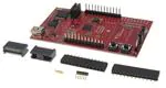
MSP-EXP430FR5739 FRAM Experimenter Board
User's Guide
Literature Number: SLAU343B
May 2011 – Revised February 2012
�2
SLAU343B – May 2011 – Revised February 2012
Submit Documentation Feedback
Copyright © 2011–2012, Texas Instruments Incorporated
�Contents
1
................................. 5
............................................................................................................... 5
1.2
Kit Contents .............................................................................................................. 6
1.3
MSP-EXP430FR5739 Board Overview ............................................................................... 6
1.4
Connecting the Hardware .............................................................................................. 6
1.5
Starting the PC GUI ..................................................................................................... 6
MSP-EXP430FR5739 User Experience Demo .......................................................................... 7
2.1
Associated Zip Folder Contents ....................................................................................... 7
2.2
The User Experience Demo ........................................................................................... 7
2.3
View, Edit, or Recompile the User Experience Code Using an IDE ............................................ 13
MSP-EXP430FR5739 Hardware ............................................................................................ 14
3.1
MSP430FR5739IRHA Device Pin Designation .................................................................... 14
3.2
Schematics ............................................................................................................. 15
3.3
PCB Layout ............................................................................................................. 18
3.4
Bill of Materials (BOM) ................................................................................................ 21
Suggested Reading ........................................................................................................... 22
References ....................................................................................................................... 22
Getting Started With the MSP-EXP430FR5739 FRAM Experimenter Board
1.1
2
3
4
5
Introduction
SLAU343B – May 2011 – Revised February 2012
Submit Documentation Feedback
Copyright © 2011–2012, Texas Instruments Incorporated
Table of Contents
3
�www.ti.com
List of Figures
1
MSP-EXP430FR5739 Overview .......................................................................................... 5
2
Comparing Write Speeds When Writing to Nonvolatile Memory (MSP430FR5739 FRAM vs
MSP430F2274 Flash) ...................................................................................................... 8
3
Comparing Average Power When Writing to Nonvolatile Memory at 13 kBps (MSP430FR5739 FRAM vs
MSP430F2274 Flash) ..................................................................................................... 10
4
On-Board Accelerometer ................................................................................................. 11
5
On-Board NTC Thermistor ............................................................................................... 12
6
MSP430FR5739 Pin Designation ....................................................................................... 14
7
Schematics (1 of 3)........................................................................................................ 15
8
Schematics (2 of 3)........................................................................................................ 16
9
Schematics (3 of 3)........................................................................................................ 17
10
MSP-EXP430FR5739 Top Layer ........................................................................................ 18
11
MSP-EXP430FR5739 Bottom Layer .................................................................................... 19
12
MSP-EXP430FR5739 Silkscreen
.......................................................................................
20
List of Tables
4
1
User Experience Source Files ........................................................................................... 13
2
Bill of Materials (BOM) .................................................................................................... 21
List of Figures
SLAU343B – May 2011 – Revised February 2012
Submit Documentation Feedback
Copyright © 2011–2012, Texas Instruments Incorporated
�User's Guide
SLAU343B – May 2011 – Revised February 2012
MSP-EXP430FR5739 FRAM Experimenter Board
1
Getting Started With the MSP-EXP430FR5739 FRAM Experimenter Board
1.1
Introduction
The MSP-EXP430FR5739 Experimenter Board introduces TI's first embedded ferro-electric random
access memory (FRAM) based MCU, the MSP430FR5739. The experimenter board is an ideal platform
for evaluating the latest in embedded memory technology while allowing the user to easily develop,
debug, and implement prototypes in an efficient manner.
The MSP430FR5739 device is supported by both IAR Embedded Workbench and Code Compose Studio.
It is recommended to download the latest version of the IDE from www.msp430.com.
The Quick Start Guide (SLAU341) is recommended for users who cannot wait to get started developing
with the MSP430FR5739. For all others, this MSP-EXP430FR5739 FRAM Experimenter Board User's
Guide provides detailed information on the hardware, the user experience firmware, and the
MSP430FR5739 device.
The MSP-EXP430FR5739 Experimenter Board is available for purchase from the TI eStore at
https://estore.ti.com/MSP-EXP430FR5739-MSP-EXP430FR5739-Experimenter-Board-P2430C42.aspx.
USB Connection
Debugging and
Programming Interface
NTC Thermistor
SBW and MSP430
Application UART
LED0 to LED8
Accelerometer
MSP430FR5739 device
Connection to CCxxxx
Daughter Cards
Connection to EXP-MSP430F5438
User Input Switches S1,S2
Reset Switch
Figure 1. MSP-EXP430FR5739 Overview
SLAU343B – May 2011 – Revised February 2012
Submit Documentation Feedback
MSP-EXP430FR5739 FRAM Experimenter Board
Copyright © 2011–2012, Texas Instruments Incorporated
5
�Getting Started With the MSP-EXP430FR5739 FRAM Experimenter Board
1.2
www.ti.com
Kit Contents
The MSP-EXP430FR5739 FRAM Experimenter Board kit includes the following:
• The MSP-EXP430FR5739 board
• Mini USB-B cable, 0.5 m
• 12-pin PCB connectors (two male and two female)
• 32.768-kHz clock crystal from Microcrystal (www.microcrystal.com)
The 32.768-kHz crystal can be used as the low-frequency XT oscillator. It is not required for the User
Experience code and can be populated as needed.
• Quick start guide
See Section 2.1 for details on the associated software and source code.
1.3
MSP-EXP430FR5739 Board Overview
The experimenter board (see Figure 1) comes equipped with the following features:
• USB debugging and programming interface that uses a driverless installation and provides an
application UART to communicate back to the PC
• On-board ADXL335 accelerometer
• NTC thermistor for temperature sensing
• Two user input switches and a reset switch
• Eight LEDs for output display
• Connectivity to the MSP-EXP430F5438 Experimenter Board
• Connectivity to CCxxx radio daughter cards
• Easily accessible device pins for debugging purposes or as socket for adding customized extension
• Separate power jumpers to measure power to the MSP430 and the RF daughter card.
1.4
Connecting the Hardware
Connect the MSP-EXP430FR5739 to the PC using the enclosed USB cable. If the PC has an MSP430
Integrated Development Environment (IDE) such as Code Composer Studio™ or IAR Embedded
Workbench™ already installed, the driver files are automatically located and installed.
If there are no IDEs installed in the PC, unzip the folder associated with this user's guide (see Section 2.1)
and point the installation to the [Install Path]\MSP-EXP430FR5739\Drivers folder.
After the drivers are installed, go to My Computer → Properties → Hardware → Device Manager to verify
that the board is enumerated under Ports COM & LPT as MSP430 Application UART.
1.5
Starting the PC GUI
The Graphical User Interface (GUI) for the PC is located in the associated zip file (see Section 2.1) under
[Install Path]\MSP-EXP430FR5739\Graphical User Interface.
Double click on FRAM_GUI.exe to load the PC application. More information on how to use this
application is provided in Section 2.
6
MSP-EXP430FR5739 FRAM Experimenter Board
SLAU343B – May 2011 – Revised February 2012
Submit Documentation Feedback
Copyright © 2011–2012, Texas Instruments Incorporated
�MSP-EXP430FR5739 User Experience Demo
www.ti.com
2
MSP-EXP430FR5739 User Experience Demo
2.1
Associated Zip Folder Contents
The zip file that contains the software and source code for the MSP-EXP430FR5739 can be downloaded
from www.ti.com/lit/zip/slac492. The contents of the zip include:
• User Experience source code and project files
• Drivers that support the board installation
• PC GUI
The design files for the experimenter board are can be downloaded from www.ti.com/lit/zip/slac502.
2.2
The User Experience Demo
The User Experience demo is pre-loaded in the MSP-EXP430FR5739 board.
The user input to the demo is given using the switches S1 and S2. These switched allow the user to
select the mode of operation and other options.
The output from the demo is displayed using the LEDs (LED1 to LED8) and is also sent via the
back-channel UART that transmits information to the PC.
There are four modes of operation for the User Experience demo:
1. High-speed FRAM writes
2. Emulating the speed of flash writes
3. Sampling accelerometer data and writing to FRAM
4. Sampling thermistor data and writing to FRAM
2.2.1
Entering and Exiting the Demo Modes
Follow these steps to enter and exit the demo modes:
1. Press switch S1 for mode selection. After you press S1, LED8 through LED5 light up to show the
corresponding mode.
2. Press switch S2 to enter the mode.
3. Press switch S2 when inside a mode to turn off the display (LED and UART output). This is useful
when measuring power.
4. Press S1 to exit a mode and return to mode selection.
NOTE: Pressing S2 without selecting a mode causes LED8 to toggle rapidly, indicating an invalid
sequence. To exit from this mode, press S1 to return to mode selection.
The MSP-EXP430FR5739 board is equipped with a reset switch. On reset, the device displays a short
LED lighting sequence.
SLAU343B – May 2011 – Revised February 2012
Submit Documentation Feedback
MSP-EXP430FR5739 FRAM Experimenter Board
Copyright © 2011–2012, Texas Instruments Incorporated
7
�MSP-EXP430FR5739 User Experience Demo
2.2.2
www.ti.com
Using Mode 1 – FRAM High Speed Writes
Mode 1 is entered by pressing S1 once, followed by S2. On entry, LED8 through LED1 light up
sequentially to display the speed of FRAM writes.
Every time the LED1 through LED8 sequence is completed, 800KB are written to FRAM. In this mode,
FRAM is bring written to at about 1.8MB per second. In comparison, a full-speed write to flash can
achieve speeds of approximately 13kB per second.
10000
Write Speed (kB/s)
1400
1000
100
13
10
1
FRAM
Flash
Figure 2. Comparing Write Speeds When Writing to Nonvolatile Memory
(MSP430FR5739 FRAM vs MSP430F2274 Flash)
Note that the code is optimized for power and not speed. FRAM memory blocks can be written at speeds
greater than 8MB per second depending on how the code is optimized. See the application report
Achieving High-Speed FRAM Writes Using the MSP430FR5739 for more details.
On entering Mode 1, the address of the FRAM scratchpad location is calculated. For the User Experience
demo, the scratchpad location starts at 0xD400 and ends at 0xF000. This location can be modified in the
header file FR_EXP.h. Note that when changing this location, it is important to first check the code space
requirements in the map file to ensure that the FRAM scratchpad area does not overlap with the
application code. Different compilers and optimization settings may impact the placement of the
application code. If any overlap occurs, the application code may be overwritten in Mode 1, which can
cause the demo to fail.
In Mode 1, the system main clock is configured to use the DCO set to 8 MHz. A function that performs
long-word writes to FRAM is called continuously inside a while loop. Each time the FRAM_Write() function
in FR_EXP.c is called, 512 bytes are written. This number was chosen arbitrarily to mimic flash segments,
and there are no restrictions on the number of FRAM bytes that can be written at once. While in Mode 1,
the LED sequence changes every time 100kB are written. For example, after the first 100KB are written,
LED8 is turned on; after the next 100kB are written, LED8 and LED7 are turned on; and so on. The
sequence completes when all eight LEDs are turned on, after which the process rolls over and starts
again from LED8.
Also, after every 100kB, a UART data transmission occurs. This data is sent to the PC via a back-channel
UART and is used to calculate the FRAM write speed and endurance information that is displayed in the
PC GUI. The raw data can also be viewed directly using a PC application such as HyperTerminal.
8
MSP-EXP430FR5739 FRAM Experimenter Board
SLAU343B – May 2011 – Revised February 2012
Submit Documentation Feedback
Copyright © 2011–2012, Texas Instruments Incorporated
�MSP-EXP430FR5739 User Experience Demo
www.ti.com
2.2.2.1
Measuring Current on the MSP-EXP430FR5739
While measuring the active power in a mode, the LEDs should be turned off and the UART transmissions
should be halted. This is done by pressing switch S2 while inside the mode. Switch S2 toggles the display
settings, turning them on or off as needed. Turning the display off allows the user to isolate and measure
the current consumption of the MSP430 device when executing instructions at a clock speed of 8 MHz
and writing to FRAM. In bench tests, the MSP430 IDVCC was measured at approximately 800 µA.
Note that, because of the nature of the FRAM cache, the number of accesses to FRAM memory can
greatly impact the active power consumption. Unoptimized code that performs a higher number of
accesses to FRAM can cause an increase in the measured current. It is advisable to review the compiler
settings when setting up a project using IDEs such as CCS or IAR to ensure the most efficient code and,
hence, the least active power.
The project that accompanies this document (see Section 2.1) uses a level 1 optimization setting in both
IAR and CCS that is one step higher than the default optimization levels.
As mentioned previously, when measuring the ICC on the board, it is important to isolate the current
consumption by the MSP430FR5739 only. The measurement can be done when the board is powered via
USB or externally via a battery. When powering via the USB, it is recommended to disconnect the
emulation portion from the MSP430FR5739 device. This can be done by removing jumpers TXD, RXD,
Reset, and Test on J3. A multimeter can be used to measure the current into the MSP430FR5739 VCC by
removing the VCC jumper and placing the multimeter leads in series.
An alternate approach requires powering the board externally via the VCC and GND connection and
disconnecting the USB cable from the board. In this case, the multimeter can be placed in series to VCC by
removing the MSP_PWR jumper.
These recommendations hold true when measuring IDVCC in all four modes.
2.2.2.2
Displaying Results on the PC GUI
The GUI associated with this document provides details on the time elapsed in the mode, number of bytes
written, speed of FRAM, and the endurance of FRAM emulated over a 512 byte FRAM block.
The endurance is calculated based on the 1014 program/erase cycles for the MSP430FR5739. Because
the GUI updates every one minute, the scale of reduction of FRAM endurance is very small. A more
obvious decline in endurance can be observed in Mode 2 when the endurance reduction when using flash
is emulated.
2.2.3
Using Mode 2 – Emulating the Speed of Flash Writes
Mode 2 is entered by pressing S1 twice, followed by S2. In this mode, the maximum speed at which flash
can be written to (at a 100% active duty cycle) is emulated on FRAM.
Similar to Mode 1, on entry into Mode 2, LED8 through LED1 light up sequentially to display the speed of
emulated flash writes. Every time the LED1 through LED8 sequence is completed, an 800KB write to flash
is emulated. In this mode, FRAM is written to at approximately 12 kBps. The entire sequence requires
approximately 80 seconds, so the demo should be observed for more than one minute to see the LED
sequence roll over.
NOTE: The time to run this sequence varies depending on the frequency source to the interval timer
(that is, the VLO).
The test uses the same scratchpad FRAM memory as Mode 1 and the same system setup. In this mode,
after every 2KB of memory is written, a UART packet is transmitted to the PC GUI to allow it to calculate
speed and endurance information.
When measuring the average power the methodology described in Section 2.2.2.1 needs to be followed.
SLAU343B – May 2011 – Revised February 2012
Submit Documentation Feedback
MSP-EXP430FR5739 FRAM Experimenter Board
Copyright © 2011–2012, Texas Instruments Incorporated
9
�MSP-EXP430FR5739 User Experience Demo
2.2.3.1
www.ti.com
The Math Behind Mode 2
The MSP430F2274 device was used as a benchmark device to calculate the maximum flash write speed.
For a 512-byte block of flash, the following parameters were obtained from the MSP430F2274 data sheet:
Segment erase time = 4819 × tFTG = 16 ms
Where, tFTG = 1 / fFTG ≈ 1 / 300 kHz
512 bytes write time ≈ 51.2 ms
Total time to write to 512 bytes ≈ 67.2 ms
Time to write to 100KB = 6.72 seconds, which calculates to 14.8 kBps
When measuring the speed of continuous flash writes on the bench, the observed speed is approximately
12 kBps, because the code execution overhead is added to the time calculated above.
This write speed is emulated with the FRAM device by maintaining a low active duty cycle and performing
one 512 byte block write every 40 ms.
Number of writes per second = 1 / 40 ms = 25
Number of bytes written per second = 512 × 25 = 12.800 kBps
The timing of the FRAM write is controlled by the VLO clock.
From these bench tests, it can be seen that writing 12 kBps to flash requires nearly 100% duty cycle,
while writing the same speed to FRAM requires less than 1% duty cycle. The rest of the time, the FRAM
device is in shutdown mode (LPM4), which results in an average current of less than 10 µA. In
comparison, for a similar write speed, flash-based MCUs can require average current up to 2.2 mA.
Power Consumption at 13 kB/s (µA)
Average power (µA)
10000
1000
100
10
1
FRAM
Flash
Figure 3. Comparing Average Power When Writing to Nonvolatile Memory at 13 kBps
(MSP430FR5739 FRAM vs MSP430F2274 Flash)
2.2.3.2
Displaying Results on the PC GUI
When in Mode 2, the GUI provides details on the time elapsed in the mode, number of bytes written,
speed of emulated flash writes, and the endurance emulated over a 512 byte flash block.
The endurance is calculated based on the 104 program/erase cycles (minimum) for the MSP430F2274. If
a 512-byte block on a flash device were written to at a speed of 12.5 kBps (that is, 25 times per second),
the endurance would exceed the minimum limit in 10000/25 or 6.6 minutes.
Note that the MSP-EXP430FR5739 board only emulates this test to demonstrate a comparison in speed
and endurance between FRAM and flash; it does not perform the test on an actual flash device.
10
MSP-EXP430FR5739 FRAM Experimenter Board
SLAU343B – May 2011 – Revised February 2012
Submit Documentation Feedback
Copyright © 2011–2012, Texas Instruments Incorporated
�MSP-EXP430FR5739 User Experience Demo
www.ti.com
Using Mode 3 – Accelerometer Demo
2.2.4
Mode 3 is entered by pressing switch S1 three times, followed by switch S2.
Upon entering this mode, the on-board accelerometer (see Figure 4) is calibrated. To aid this calibration
process, it is recommended to place the board on a level surface before entering the mode.
3 Axis Accelerometer
Figure 4. On-Board Accelerometer
After the calibration sequence is completed, LED4 and LED5 are turned on. When tilting the board in an
upward or downward direction, the LEDs follow the direction of the tilt. S2 toggles the display on and off,
similar to other modes.
Mode 3 also writes the sampled data from the ADC to the FRAM in real time with no wait states or extra
cycles spent on setting up the FRAM. This can be observed in the ADC interrupt service routine. The
sampling takes place at more than 15k samples per second. At this speed, flash devices require that the
data be buffered in RAM before writing to flash. In FRAM devices, the only bottleneck is the speed at
which the ADC can sample, not the writes to nonvolatile memory.
2.2.4.1
Displaying Results on the PC GUI
When in the accelerometer mode, the GUI mimics the LEDs that are lit up on the Experimenter Board and
are a reflection of the tilt of the board.
SLAU343B – May 2011 – Revised February 2012
Submit Documentation Feedback
MSP-EXP430FR5739 FRAM Experimenter Board
Copyright © 2011–2012, Texas Instruments Incorporated
11
�MSP-EXP430FR5739 User Experience Demo
www.ti.com
Using Mode 4 – Temperature Sensor Demo
2.2.5
Mode 4 is entered by pressing switch S1 four times, followed by switch S2.
Upon entering this mode, the on-board thermistor (see Figure 5) is calibrated.
NTC Thermistor
Figure 5. On-Board NTC Thermistor
After the calibration sequence is completed, LED4 and LED5 are turned on. When the NTC resistor is
heated (for example, by placing a finger on it), LED3 through LED1 are turned on sequentially. When the
NTC is cooled (for example, by using a freeze spay or a keyboard dust remover that uses compressed air)
LED5 through LED8 are turned on sequentially.
Similar to Mode 3, Mode 4 also writes the sampled data from the ADC to the FRAM in real time with no
wait states or extra cycles spent on setting up the FRAM. This can be observed in the ADC interrupt
service routine. The sampling takes place at more than 15k samples per second. At this speed, flash
devices require that the data be buffered in RAM before writing to flash. In FRAM devices, the only
bottleneck is the speed at which the ADC can sample, not the writes to nonvolatile memory.
2.2.5.1
Displaying Results on the PC GUI
When in the temperature sense mode, the GUI mimics the LEDs that are lit up on the Experimenter Board
and are a reflection of the thermistor's ambient temperature measurement.
12
MSP-EXP430FR5739 FRAM Experimenter Board
SLAU343B – May 2011 – Revised February 2012
Submit Documentation Feedback
Copyright © 2011–2012, Texas Instruments Incorporated
�MSP-EXP430FR5739 User Experience Demo
www.ti.com
2.3
View, Edit, or Recompile the User Experience Code Using an IDE
There are different development software tools available for the MSP-EXP430FR5739 board. IAR
Embedded Workbench™ KickStart™ and Code Composer Studio™ (CCS) IDEs are both available in a
free limited version. IAR Embedded Workbench allows 4KB of C-code compilation. CCS is limited to a
code size of 16KB. The software is available at www.ti.com/msp430.
To view, modify, or edit the User Experience code provided with the MSP-EXP430FR5739, an IDE
installation is required. The associated software package (see Section 2.1) supports both IAR and CCS
projects.
The User Experience source files and project folders are provided in the folder [Install
Path]\MSP-EXP430FR5739\MSP-EXP430FR5739 User Experience.
2.3.1
Setting up the IAR Workspace for the User Experience Code
To
1.
2.
3.
set up the IAR workspace for the User Experience demo source code:
Double-click and open MSP-EXP430FR5739_Workspace.eww in IAR.
The Project is automatically included in the workspace.
Click Project → Download & Debug to download the code to the MSP-EXP430FR5739 Experimenter
Board.
4. If multiple emulation tools are connected to your PC, click Project → Options → FET Debugger →
Connection to explicitly select the experimenter board.
2.3.2
Importing the CCS Project for the User Experience Code
To
1.
2.
3.
4.
import the CCS project for the User Experience demo source code:
Create a workspace folder.
Open CCS and point to the newly created workspace folder.
Click Project → Import Existing CCS/CCE Eclipse Project.
Browse to the folder [Install Path]\MSP-EXP430FR5739\MSP-EXP430FR5739 User Experience that
was extracted from the associated zip file (see Section 2.1).
5. The project MSP-EXP430FR5739_UserExperience is automatically selected.
6. Click Finish to include the project in the current workspace.
7. Click the Debug icon to download the project
2.3.3
Source Files
Table 1 describes the source files for the User Experience demo.
Table 1. User Experience Source Files
Name
Description
Main.c
This file contains the user experience demo
Main.h
This file contains the definitions that are required for main.c
FR_EXP.c
This file contains the definitions of all C functions used by main.c
FR_EXP.h
This file contains all the function declarations needed by main.c and FR_EXP.c
SLAU343B – May 2011 – Revised February 2012
Submit Documentation Feedback
MSP-EXP430FR5739 FRAM Experimenter Board
Copyright © 2011–2012, Texas Instruments Incorporated
13
�MSP-EXP430FR5739 Hardware
www.ti.com
3
MSP-EXP430FR5739 Hardware
3.1
MSP430FR5739IRHA Device Pin Designation
See the MSP430FR5739 data sheet (SLAS639) for the latest information.
RHA PACKAGE
(TOP VIEW)
P2.4/TA1.0/UCA1CLK/A7*/CD11
P2.3/TA0.0/UCA1STE/A6*/CD10
P2.7
DVCC
DVSS
31
32
33
35
34
36
37
39
30
1
2
29
MSP430FR5721
MSP430FR5723
MSP430FR5725
MSP430FR5727
MSP430FR5729
MSP430FR5731
MSP430FR5733
MSP430FR5735
MSP430FR5737
MSP430FR5739
3
4
5
6
7
8
9
28
27
26
25
24
23
22
10
PJ.0/TDO/TB0OUTH/SMCLK/CD6
PJ.1/TDI/TCLK/TB1OUTH/MCLK/CD7
PJ.2/TMS/TB2OUTH/ACLK/CD8
PJ.3/TCK/CD9
P4.0/TB2.0
VCORE
P1.7/TB1.2/UCB0SOMI/UCB0SCL/TA1.0
P1.6/TB1.1/UCB0SIMO/UCB0SDA/TA0.0
P3.7/TB2.2
P3.6/TB2.1/TB1CLK
P3.5/TB1.2/CDOUT
P3.4/TB1.1/TB2CLK/SMCLK
P2.2/TB2.2/UCB0CLK/TB1.0
P2.1/TB2.1/UCA0RXD/UCA0SOMI/TB0.0
P2.0/TB2.0/UCA0TXD/UCA0SIMO/TB0CLK/ACLK
20
19
18
17
16
15
14
13
11
21
12
P1.0/TA0.1/DMAE0/RTCCLK/A0*/CD0/VeREF-*
P1.1/TA0.2/TA1CLK/CDOUT/A1*/CD1/VeREF+*
P1.2/TA1.1/TA0CLK/CDOUT/A2*/CD2
P3.0/A12*/CD12
P3.1/A13*/CD13
P3.2/A14*/CD14
P3.3/A15*/CD15
P1.3/TA1.2/UCB0STE/A3*/CD3
P1.4/TB0.1/UCA0STE/A4*/CD4
P1.5/TB0.2/UCA0CLK/A5*/CD5
38
40
AVSS
PJ.4/XIN
PJ.5/XOUT
AVSS
AVCC
RST/NMI/SBWTDIO
TEST/SBWTCK
P2.6/TB1.0/UCA1RXD/UCA1SOMI
P2.5/TB0.0/UCA1TXD/UCA1SIMO
P4.1
* Not available on MSP430FR5737, MSP430FR5733, MSP430FR5727, MSP430FR5723
Note: Power Pad connection to VSS recommended.
Figure 6. MSP430FR5739 Pin Designation
14
MSP-EXP430FR5739 FRAM Experimenter Board
SLAU343B – May 2011 – Revised February 2012
Submit Documentation Feedback
Copyright © 2011–2012, Texas Instruments Incorporated
�TP6 TP4 TP2
TP7 TP5 TP3 TP1
GND
GND
SLAU343B – May 2011 – Revised February 2012
Submit Documentation Feedback
LED0
green
GND
R26
270
EZ_VCC
1u/6.3V
C4
URTS
UDTR
UDSR
UCTS
100n
C5
1
2
3
4
5
6
7
8
9
10
11
12
13
14
15
16
C1
10n
RESET
R1
47k
16p
C2
12MHz
Q1
16p
C3
EZ_VCC
64
63
62
61
60
59
58
57
56
55
54
53
52
51
50
49
48
47
46
45
44
43
42
41
40
39
38
37
36
35
34
33
R3
47k
SCL
SDA
BRXDI
BTXDI
URXD
UTXD
RST3410
R2
47k
GND
100R
100R
100R
100R
J3
9
7
5
3
1
P2.0
EZ_VCC
SBWTCK
SBWTDIO
GND
P2.1
1
2
3
4
5
6
Copyright © 2011–2012, Texas Instruments Incorporated
MSP-EXP430G2 EMULATOR 1/2
SL127L6TH
J4
1.4
TEST/SBWTCK
RST/SBWTDIO
P2.1
P2.0
VCC
SBW & UART I/F to external Ta rget
10
8
6
4
2
SBW & UART I/F to Argon
SBWTCK
SBWTDIO
BTXD
BRXD
EZ_VCC
Removed U2: SN75240PW from SBW connections
R6
R7
R4
R5
CLK3410
EZ_VCC
3.2
17
18
19
20
21
22
23
24
25
26
27
28
29
30
31
32
EZ_VBUS
RESET
GND
HTCK
HTMS
HTDI
HTDO
www.ti.com
MSP-EXP430FR5739 Hardware
Schematics
The schematics and PCB layouts for the MSP-EXP430FR5739 are shown in the following pages.
Figure 7. Schematics (1 of 3)
MSP-EXP430FR5739 FRAM Experimenter Board
15
�MSP-EXP430FR5739 FRAM Experimenter Board
C8
R16
47k
EZ_VCC
Copyright © 2011–2012, Texas Instruments Incorporated
R11
15k
R25
1k5
R23
100R
EZ_VCC
UTXD
URXD
R17 DNP
47k
R10
10k
R24
1k5
SCL
SDA
CLK3410
BRXDI
BTXDI
DNP
GND
1u/6.3V
RST3410
EZ_VCC
D1
1N4148
33k
GND
R22
3k3
3k3
R19
R12
X1
X2
4
3
2
1
SDA
SCL
P3.0
P3.1
P3.3
P3.4
SIN
SOUT
U3
WC
SCL
SDA
C13
100n
CAT24FC32UI
VSS VCC
E2
E1
E0
U5
TUSB3410VF
VREGEN
RESET
WAKEUP
SUSPEND
CLKOUT
GND
27
26
10
11
32
31
30
29
17
19
1
9
12
2
22
8
7
6
5
100n
C11
CTS
DSR
DCD
RI/CP
RTS
DTR
TEST0
TEST1
VCC
VCC1
VDD18
GND
GND1
GND2
PUR
DP
DM
GND
GND
R13 1k5
EZ_VCC
C12
100n
13
14
15
16
20
21
23
24
3
25
4
8
18
28
5
6
7
URTS
UDTR
EZ_VCC
UCTS
UDSR
R20
100k/1%
R18
100k/1%
GND
C9
22p
GND
GND ND
C10
22p
R14
4
3
U2
FB
RESET
TPS77301DGK
EN
GND RES
IN2 OUT2
IN1 OUT1
G
1
2
7
8
R21
33k
3
EZ_D+
S4
S3
S2
S1
5
4
1
2
EZ_D-
GND
1.4
USB_MINI_B5
SHIELD4
SHIELD3
SHIELD2
SHIELD1
GND
ID
D+
D-
VBUS
Mini USB
Connector
U$2
1u/6.3V
C6
EZ_VCC
EZ_VBUS
GND
33k
R9
61k5
R8
VCC = +3.6V
MSP-EXP430G2 EMULATOR 2/2
GND
33R
R15 33R
GND
C7
100n
6
5
4
2
5
3
1
16
GND
NC
IO2
IO1
VCC
EZ_VBUS
MSP-EXP430FR5739 Hardware
www.ti.com
Figure 8. Schematics (2 of 3)
SLAU343B – May 2011 – Revised February 2012
Submit Documentation Feedback
�S1
J6
S2
2
GND
.1u
P3.2
C58
GND
GND
VCC
Ext_PWR
DNP
C22 XINR
12pF
DNP
C21 XOUTR
12pF
10uF/10V
C23
2
1
GND
2
1
2
3
4
5
6
7
8
DNP
2 or 3-Axis
Accelerometer
GND
P3.3
16
15
14
13
12
11
10
9
P2.7
NC
VS
VS
NC
XOUT
NC
YOUT
NC
ADXL322/330
NC
ST
COM
NC
COM
COM
COM
ZOUT
4.7u
C53
R34
1
ACC
.1u
C15
R35
P1.4
GND
PJ.0
PJ.1
GND
.
.1u 1u
GND
7 C1
P3.1
P3.0
C16
P2.7
GND
PJ.2
GND
PJ.3
SV1
P4.0
P2.0
P1.0
RFPWR
RFPWR
1
2
3
4
5
6
7
8
9
10
11
12
GND
GND
R37
1
1
2
3
GND
0R
RST
C20
100nF
QUARZ5
Q2
LDR
XT1_GND
470k
100k
GND
330
NTC
RF1
R29
LED1
GND
330
P1.1
P1.2
P4.1
P2.3
P1.3
P2.2
P1.6
P1.7
R28
LED2
1
3
5
7
9
11
13
15
17
19
P3.4
P1
P1.0
P1.1
P1.2
P3.0
P3.1
P3.2
P3.3
P1.3
P1.4
P1.5
P4.0
GND
TP8
VCC
RF2
2
4
6
8
10
12
14
16
18
20
P3.5
GND
TP9
P3.6
TP10
TP11
TP12
TP13
VCC_MSP
P2.7
P3.7
GND
GND
R31
P2.4
P1.0
P1.1
P1.2
330
2
4
6
8
10
12
14
16
18
20
R36
LED3
R27
LED5
1 MSP_PWR
2
330
P3.7
R32
GND GND
1
2
3
4
5
6
7
8
9
10
TP17
RFPWR
P1.0
P1.1
P1.2
P2.3
GND
P2.4
P2.2
P1.6
2
4
6
8
10
12
14
16
18
RF3
eZ-RF
1
3
5
7
9
11
13
15
17
PJ.0
PJ.1
PJ.2
PJ.3
0.1u
GND
P2.0
P2.6
P2.5
P2.7
P4.0
P4.1
P1.7
P1.3
FR57xx Fraunchpad
TEST/SBWTCK
RST/SBWTDIO
30
29
28
27
26
25
24
23
22
21
GND GND
30_VCORE
1_P1.0
2_P1.1
29_P1.7
28_P1.6
3_P1.2 FR57XX--RHA40RHAPACKAGE
4_P3.0 FR57XX
27_P3.7
5_P3.1
26_P3.6
25_P3.5
6_P3.2
24_P3.4
7_P3.3
23_P2.2
8_P1.3
9_P1.4
22_P2.1
10_P1.5
21_P2.0
P4.1
1
3
5
7
9
11
13
15
17
19
330
GND
TP
41_TP
C18
RST/SBWTDIO
330
LED4
R30
LED6
11
12
13
14
15
16
17
18
19
20
C19
P4.1
330
40 VCC_MSP
39 GND
38 XOUTR
37 XINR
36 GND
35 P2.4
34 P2.3
33 P2.7
32 VCC_MSP
31 GND
40_AVCC
39_AVSS
38_PJ.5
37_PJ.4
36_AVSS
35_P2.4
34_P2.3
33_P2.7
32_DVCC
31_DVSS
11_PJ.0_TDO
12_PJ.1_TDI_TCLK
13_PJ.2_TMS
14_PJ.3_TCK
15_P4.0
16_P4.1
17_P2.5
18_P2.6
19_TEST_SBWTCK
20__RST_SBWTDIO
470n
GND
2.2n
C24
VCC_MSP
C14
VCORE
10u
R33
RF_PWR
RF_PWR
.1u
TP14
TP15
TP16
P1.7
P1.6
P3.7
P3.6
P3.5
P3.4
P2.2
P2.1
P2.6
P2.5
P2.0
VCC
GND
C31
4.7u
2
1
C32
GND
P4.0
330
Copyright © 2011–2012, Texas Instruments Incorporated
LED7
47k
SLAU343B – May 2011 – Revised February 2012
Submit Documentation Feedback
LED8
SV2
1.0
1
2
3
4
5
6
7
8
9
10
11
12
VCC
www.ti.com
MSP-EXP430FR5739 Hardware
Figure 9. Schematics (3 of 3)
MSP-EXP430FR5739 FRAM Experimenter Board
17
�MSP-EXP430FR5739 Hardware
3.3
www.ti.com
PCB Layout
Figure 10. MSP-EXP430FR5739 Top Layer
18
MSP-EXP430FR5739 FRAM Experimenter Board
SLAU343B – May 2011 – Revised February 2012
Submit Documentation Feedback
Copyright © 2011–2012, Texas Instruments Incorporated
�MSP-EXP430FR5739 Hardware
www.ti.com
Figure 11. MSP-EXP430FR5739 Bottom Layer
SLAU343B – May 2011 – Revised February 2012
Submit Documentation Feedback
MSP-EXP430FR5739 FRAM Experimenter Board
Copyright © 2011–2012, Texas Instruments Incorporated
19
�MSP-EXP430FR5739 Hardware
www.ti.com
Figure 12. MSP-EXP430FR5739 Silkscreen
20
MSP-EXP430FR5739 FRAM Experimenter Board
SLAU343B – May 2011 – Revised February 2012
Submit Documentation Feedback
Copyright © 2011–2012, Texas Instruments Incorporated
�MSP-EXP430FR5739 Hardware
www.ti.com
3.4
Bill of Materials (BOM)
Table 2 shows the bill of materials for the MSP-EXP430FR5739 board.
Table 2. Bill of Materials (BOM)
Ref Des
Numbe
r per
Board
1
C1
1
10n
2
C2,C3
2
16p
3
C4, C6, C8
3
1u/6.3V
4
C5, C7, C11,
C12,C13
5
100n
5
C15, C16, C17,
C18, C20, C31,
C58
7
100n
6
C9, C10
2
22p
7
C14
1
470n
8
C19
1
10u
Pos.
Description
9
C21, C22
0
12pF
10
C23
1
10uF/10V
11
C24
1
2.2nF
12
C32, C53
2
4.7u
13
D1
1
1N4148
14
FR5739
1
FR5739-RHA40
15
J3
1
2x05 Pin Header Male
16
J4
[1]
SL127L6TH
17
J6
1
3-pin header, male, TH
18
LDR
0
Do not populate
19
LED0
1
LED GREEN 0603
20
LED1 - LED8
8
LED BLUE 470NM 0603 SMD
21
MSP_PWR
1
2-pin header, male, TH
22
NTC
1
100k
23
Q1
1
12MHz
24
Q2
1
Crystal
25
R1, R2, R3, R16,
R17, R33
4
47k
26
R4, R5, R6, R7,
R23
4
100R
27
R8
1
61k5
28
R12
1
33k
29
R9
1
30K
30
R10
1
10k
31
R11
1
15k
32
R13, R24, R25
3
1k5
33
R14, R15
2
33R
35
R18, R20
2
100k/1%
36
R19, R22
2
3k3
37
R21
1
33k
39
R26
1
270
34
SLAU343B – May 2011 – Revised February 2012
Submit Documentation Feedback
MSP-EXP430FR5739 FRAM Experimenter Board
Copyright © 2011–2012, Texas Instruments Incorporated
21
�Suggested Reading
www.ti.com
Table 2. Bill of Materials (BOM) (continued)
4
Pos.
Ref Des
Numbe
r per
Board
40
R27, R28, R29,
R30, R31, R32,
R36, R37
8
330
41
R34
0
0R
42
R35
1
470k
43
RF1, RF2
2
44
RF3
0
eZ-RF connector for EXP-F5438 board
45
RF_PWR
1
RF_PWR
46
S1, S2
2
47
RST
1
48
SV1, SV2
2+[2]
49
U$2
1
USB_MINI_B5
50
U1
1
F1612-PM64
51
U2
1
TPS77301DGK
52
U3
1
TUSB3410VF
53
U4
1
TPD2E001
54
U5
1
CAT24FC32UI
55
U6
1
ADXL335 accelerometer
Description
12-pin header, TH
Suggested Reading
The primary sources of MSP430 information are the device-specific data sheets and user's guides. The
most up-to-date versions of those documents can be found at the Texas Instruments MSP430 page
www.ti.com/msp430.
Visit www.ti.com/fram to find the latest information on TI's FRAM family.
To get an inside view of the CCS and IAR IDEs, download the latest version from the MSP430 page and
read the included user's guides and documentation in the installation folder.
Documents describing the IAR tools (Workbench/C-SPY, the assembler, the C compiler, the linker, and
the library) are located in common\doc and 430\doc. All necessary CCS documents can be found in
msp430\doc inside the CCS installation path. The Code Composer Studio v4.2 for MSP430™ User’s
Guide (SLAU157) and IAR Embedded Workbench Version 3+ for MSP430™ User's Guide (SLAU138)
include detailed information on how to set up a project for the MSP430 using CCS or IAR. They are
included in most of the IDE releases and on the MSP430 page.
5
References
1. MSP430FR5739 data sheet (SLAS639)
2. MSP430F2274 data sheet (SLAS504)
3. MSP430FR57xx Family User's Guide (SLAU272)
22
MSP-EXP430FR5739 FRAM Experimenter Board
SLAU343B – May 2011 – Revised February 2012
Submit Documentation Feedback
Copyright © 2011–2012, Texas Instruments Incorporated
�STANDARD TERMS FOR EVALUATION MODULES
1.
Delivery: TI delivers TI evaluation boards, kits, or modules, including any accompanying demonstration software, components, and/or
documentation which may be provided together or separately (collectively, an “EVM” or “EVMs”) to the User (“User”) in accordance
with the terms set forth herein. User's acceptance of the EVM is expressly subject to the following terms.
1.1 EVMs are intended solely for product or software developers for use in a research and development setting to facilitate feasibility
evaluation, experimentation, or scientific analysis of TI semiconductors products. EVMs have no direct function and are not
finished products. EVMs shall not be directly or indirectly assembled as a part or subassembly in any finished product. For
clarification, any software or software tools provided with the EVM (“Software”) shall not be subject to the terms and conditions
set forth herein but rather shall be subject to the applicable terms that accompany such Software
1.2 EVMs are not intended for consumer or household use. EVMs may not be sold, sublicensed, leased, rented, loaned, assigned,
or otherwise distributed for commercial purposes by Users, in whole or in part, or used in any finished product or production
system.
2
Limited Warranty and Related Remedies/Disclaimers:
2.1 These terms do not apply to Software. The warranty, if any, for Software is covered in the applicable Software License
Agreement.
2.2 TI warrants that the TI EVM will conform to TI's published specifications for ninety (90) days after the date TI delivers such EVM
to User. Notwithstanding the foregoing, TI shall not be liable for a nonconforming EVM if (a) the nonconformity was caused by
neglect, misuse or mistreatment by an entity other than TI, including improper installation or testing, or for any EVMs that have
been altered or modified in any way by an entity other than TI, (b) the nonconformity resulted from User's design, specifications
or instructions for such EVMs or improper system design, or (c) User has not paid on time. Testing and other quality control
techniques are used to the extent TI deems necessary. TI does not test all parameters of each EVM.
User's claims against TI under this Section 2 are void if User fails to notify TI of any apparent defects in the EVMs within ten (10)
business days after delivery, or of any hidden defects with ten (10) business days after the defect has been detected.
2.3 TI's sole liability shall be at its option to repair or replace EVMs that fail to conform to the warranty set forth above, or credit
User's account for such EVM. TI's liability under this warranty shall be limited to EVMs that are returned during the warranty
period to the address designated by TI and that are determined by TI not to conform to such warranty. If TI elects to repair or
replace such EVM, TI shall have a reasonable time to repair such EVM or provide replacements. Repaired EVMs shall be
warranted for the remainder of the original warranty period. Replaced EVMs shall be warranted for a new full ninety (90) day
warranty period.
WARNING
Evaluation Kits are intended solely for use by technically qualified,
professional electronics experts who are familiar with the dangers
and application risks associated with handling electrical mechanical
components, systems, and subsystems.
User shall operate the Evaluation Kit within TI’s recommended
guidelines and any applicable legal or environmental requirements
as well as reasonable and customary safeguards. Failure to set up
and/or operate the Evaluation Kit within TI’s recommended
guidelines may result in personal injury or death or property
damage. Proper set up entails following TI’s instructions for
electrical ratings of interface circuits such as input, output and
electrical loads.
NOTE:
EXPOSURE TO ELECTROSTATIC DISCHARGE (ESD) MAY CAUSE DEGREDATION OR FAILURE OF THE EVALUATION
KIT; TI RECOMMENDS STORAGE OF THE EVALUATION KIT IN A PROTECTIVE ESD BAG.
�www.ti.com
3
Regulatory Notices:
3.1 United States
3.1.1
Notice applicable to EVMs not FCC-Approved:
FCC NOTICE: This kit is designed to allow product developers to evaluate electronic components, circuitry, or software
associated with the kit to determine whether to incorporate such items in a finished product and software developers to write
software applications for use with the end product. This kit is not a finished product and when assembled may not be resold or
otherwise marketed unless all required FCC equipment authorizations are first obtained. Operation is subject to the condition
that this product not cause harmful interference to licensed radio stations and that this product accept harmful interference.
Unless the assembled kit is designed to operate under part 15, part 18 or part 95 of this chapter, the operator of the kit must
operate under the authority of an FCC license holder or must secure an experimental authorization under part 5 of this chapter.
3.1.2
For EVMs annotated as FCC – FEDERAL COMMUNICATIONS COMMISSION Part 15 Compliant:
CAUTION
This device complies with part 15 of the FCC Rules. Operation is subject to the following two conditions: (1) This device may not
cause harmful interference, and (2) this device must accept any interference received, including interference that may cause
undesired operation.
Changes or modifications not expressly approved by the party responsible for compliance could void the user's authority to
operate the equipment.
FCC Interference Statement for Class A EVM devices
NOTE: This equipment has been tested and found to comply with the limits for a Class A digital device, pursuant to part 15 of
the FCC Rules. These limits are designed to provide reasonable protection against harmful interference when the equipment is
operated in a commercial environment. This equipment generates, uses, and can radiate radio frequency energy and, if not
installed and used in accordance with the instruction manual, may cause harmful interference to radio communications.
Operation of this equipment in a residential area is likely to cause harmful interference in which case the user will be required to
correct the interference at his own expense.
FCC Interference Statement for Class B EVM devices
NOTE: This equipment has been tested and found to comply with the limits for a Class B digital device, pursuant to part 15 of
the FCC Rules. These limits are designed to provide reasonable protection against harmful interference in a residential
installation. This equipment generates, uses and can radiate radio frequency energy and, if not installed and used in accordance
with the instructions, may cause harmful interference to radio communications. However, there is no guarantee that interference
will not occur in a particular installation. If this equipment does cause harmful interference to radio or television reception, which
can be determined by turning the equipment off and on, the user is encouraged to try to correct the interference by one or more
of the following measures:
•
•
•
•
Reorient or relocate the receiving antenna.
Increase the separation between the equipment and receiver.
Connect the equipment into an outlet on a circuit different from that to which the receiver is connected.
Consult the dealer or an experienced radio/TV technician for help.
3.2 Canada
3.2.1
For EVMs issued with an Industry Canada Certificate of Conformance to RSS-210 or RSS-247
Concerning EVMs Including Radio Transmitters:
This device complies with Industry Canada license-exempt RSSs. Operation is subject to the following two conditions:
(1) this device may not cause interference, and (2) this device must accept any interference, including interference that may
cause undesired operation of the device.
Concernant les EVMs avec appareils radio:
Le présent appareil est conforme aux CNR d'Industrie Canada applicables aux appareils radio exempts de licence. L'exploitation
est autorisée aux deux conditions suivantes: (1) l'appareil ne doit pas produire de brouillage, et (2) l'utilisateur de l'appareil doit
accepter tout brouillage radioélectrique subi, même si le brouillage est susceptible d'en compromettre le fonctionnement.
Concerning EVMs Including Detachable Antennas:
Under Industry Canada regulations, this radio transmitter may only operate using an antenna of a type and maximum (or lesser)
gain approved for the transmitter by Industry Canada. To reduce potential radio interference to other users, the antenna type
and its gain should be so chosen that the equivalent isotropically radiated power (e.i.r.p.) is not more than that necessary for
successful communication. This radio transmitter has been approved by Industry Canada to operate with the antenna types
listed in the user guide with the maximum permissible gain and required antenna impedance for each antenna type indicated.
Antenna types not included in this list, having a gain greater than the maximum gain indicated for that type, are strictly prohibited
for use with this device.
2
�www.ti.com
Concernant les EVMs avec antennes détachables
Conformément à la réglementation d'Industrie Canada, le présent émetteur radio peut fonctionner avec une antenne d'un type et
d'un gain maximal (ou inférieur) approuvé pour l'émetteur par Industrie Canada. Dans le but de réduire les risques de brouillage
radioélectrique à l'intention des autres utilisateurs, il faut choisir le type d'antenne et son gain de sorte que la puissance isotrope
rayonnée équivalente (p.i.r.e.) ne dépasse pas l'intensité nécessaire à l'établissement d'une communication satisfaisante. Le
présent émetteur radio a été approuvé par Industrie Canada pour fonctionner avec les types d'antenne énumérés dans le
manuel d’usage et ayant un gain admissible maximal et l'impédance requise pour chaque type d'antenne. Les types d'antenne
non inclus dans cette liste, ou dont le gain est supérieur au gain maximal indiqué, sont strictement interdits pour l'exploitation de
l'émetteur
3.3 Japan
3.3.1
Notice for EVMs delivered in Japan: Please see http://www.tij.co.jp/lsds/ti_ja/general/eStore/notice_01.page 日本国内に
輸入される評価用キット、ボードについては、次のところをご覧ください。
http://www.tij.co.jp/lsds/ti_ja/general/eStore/notice_01.page
3.3.2
Notice for Users of EVMs Considered “Radio Frequency Products” in Japan: EVMs entering Japan may not be certified
by TI as conforming to Technical Regulations of Radio Law of Japan.
If User uses EVMs in Japan, not certified to Technical Regulations of Radio Law of Japan, User is required to follow the
instructions set forth by Radio Law of Japan, which includes, but is not limited to, the instructions below with respect to EVMs
(which for the avoidance of doubt are stated strictly for convenience and should be verified by User):
1.
2.
3.
Use EVMs in a shielded room or any other test facility as defined in the notification #173 issued by Ministry of Internal
Affairs and Communications on March 28, 2006, based on Sub-section 1.1 of Article 6 of the Ministry’s Rule for
Enforcement of Radio Law of Japan,
Use EVMs only after User obtains the license of Test Radio Station as provided in Radio Law of Japan with respect to
EVMs, or
Use of EVMs only after User obtains the Technical Regulations Conformity Certification as provided in Radio Law of Japan
with respect to EVMs. Also, do not transfer EVMs, unless User gives the same notice above to the transferee. Please note
that if User does not follow the instructions above, User will be subject to penalties of Radio Law of Japan.
【無線電波を送信する製品の開発キットをお使いになる際の注意事項】 開発キットの中には技術基準適合証明を受けて
いないものがあります。 技術適合証明を受けていないもののご使用に際しては、電波法遵守のため、以下のいずれかの
措置を取っていただく必要がありますのでご注意ください。
1.
2.
3.
電波法施行規則第6条第1項第1号に基づく平成18年3月28日総務省告示第173号で定められた電波暗室等の試験設備でご使用
いただく。
実験局の免許を取得後ご使用いただく。
技術基準適合証明を取得後ご使用いただく。
なお、本製品は、上記の「ご使用にあたっての注意」を譲渡先、移転先に通知しない限り、譲渡、移転できないものとします。
上記を遵守頂けない場合は、電波法の罰則が適用される可能性があることをご留意ください。 日本テキサス・イ
ンスツルメンツ株式会社
東京都新宿区西新宿6丁目24番1号
西新宿三井ビル
3.3.3
Notice for EVMs for Power Line Communication: Please see http://www.tij.co.jp/lsds/ti_ja/general/eStore/notice_02.page
電力線搬送波通信についての開発キットをお使いになる際の注意事項については、次のところをご覧ください。http:/
/www.tij.co.jp/lsds/ti_ja/general/eStore/notice_02.page
3.4 European Union
3.4.1
For EVMs subject to EU Directive 2014/30/EU (Electromagnetic Compatibility Directive):
This is a class A product intended for use in environments other than domestic environments that are connected to a
low-voltage power-supply network that supplies buildings used for domestic purposes. In a domestic environment this
product may cause radio interference in which case the user may be required to take adequate measures.
3
�www.ti.com
4
EVM Use Restrictions and Warnings:
4.1 EVMS ARE NOT FOR USE IN FUNCTIONAL SAFETY AND/OR SAFETY CRITICAL EVALUATIONS, INCLUDING BUT NOT
LIMITED TO EVALUATIONS OF LIFE SUPPORT APPLICATIONS.
4.2 User must read and apply the user guide and other available documentation provided by TI regarding the EVM prior to handling
or using the EVM, including without limitation any warning or restriction notices. The notices contain important safety information
related to, for example, temperatures and voltages.
4.3 Safety-Related Warnings and Restrictions:
4.3.1
User shall operate the EVM within TI’s recommended specifications and environmental considerations stated in the user
guide, other available documentation provided by TI, and any other applicable requirements and employ reasonable and
customary safeguards. Exceeding the specified performance ratings and specifications (including but not limited to input
and output voltage, current, power, and environmental ranges) for the EVM may cause personal injury or death, or
property damage. If there are questions concerning performance ratings and specifications, User should contact a TI
field representative prior to connecting interface electronics including input power and intended loads. Any loads applied
outside of the specified output range may also result in unintended and/or inaccurate operation and/or possible
permanent damage to the EVM and/or interface electronics. Please consult the EVM user guide prior to connecting any
load to the EVM output. If there is uncertainty as to the load specification, please contact a TI field representative.
During normal operation, even with the inputs and outputs kept within the specified allowable ranges, some circuit
components may have elevated case temperatures. These components include but are not limited to linear regulators,
switching transistors, pass transistors, current sense resistors, and heat sinks, which can be identified using the
information in the associated documentation. When working with the EVM, please be aware that the EVM may become
very warm.
4.3.2
EVMs are intended solely for use by technically qualified, professional electronics experts who are familiar with the
dangers and application risks associated with handling electrical mechanical components, systems, and subsystems.
User assumes all responsibility and liability for proper and safe handling and use of the EVM by User or its employees,
affiliates, contractors or designees. User assumes all responsibility and liability to ensure that any interfaces (electronic
and/or mechanical) between the EVM and any human body are designed with suitable isolation and means to safely
limit accessible leakage currents to minimize the risk of electrical shock hazard. User assumes all responsibility and
liability for any improper or unsafe handling or use of the EVM by User or its employees, affiliates, contractors or
designees.
4.4 User assumes all responsibility and liability to determine whether the EVM is subject to any applicable international, federal,
state, or local laws and regulations related to User’s handling and use of the EVM and, if applicable, User assumes all
responsibility and liability for compliance in all respects with such laws and regulations. User assumes all responsibility and
liability for proper disposal and recycling of the EVM consistent with all applicable international, federal, state, and local
requirements.
5.
Accuracy of Information: To the extent TI provides information on the availability and function of EVMs, TI attempts to be as accurate
as possible. However, TI does not warrant the accuracy of EVM descriptions, EVM availability or other information on its websites as
accurate, complete, reliable, current, or error-free.
6.
Disclaimers:
6.1 EXCEPT AS SET FORTH ABOVE, EVMS AND ANY MATERIALS PROVIDED WITH THE EVM (INCLUDING, BUT NOT
LIMITED TO, REFERENCE DESIGNS AND THE DESIGN OF THE EVM ITSELF) ARE PROVIDED "AS IS" AND "WITH ALL
FAULTS." TI DISCLAIMS ALL OTHER WARRANTIES, EXPRESS OR IMPLIED, REGARDING SUCH ITEMS, INCLUDING BUT
NOT LIMITED TO ANY EPIDEMIC FAILURE WARRANTY OR IMPLIED WARRANTIES OF MERCHANTABILITY OR FITNESS
FOR A PARTICULAR PURPOSE OR NON-INFRINGEMENT OF ANY THIRD PARTY PATENTS, COPYRIGHTS, TRADE
SECRETS OR OTHER INTELLECTUAL PROPERTY RIGHTS.
6.2 EXCEPT FOR THE LIMITED RIGHT TO USE THE EVM SET FORTH HEREIN, NOTHING IN THESE TERMS SHALL BE
CONSTRUED AS GRANTING OR CONFERRING ANY RIGHTS BY LICENSE, PATENT, OR ANY OTHER INDUSTRIAL OR
INTELLECTUAL PROPERTY RIGHT OF TI, ITS SUPPLIERS/LICENSORS OR ANY OTHER THIRD PARTY, TO USE THE
EVM IN ANY FINISHED END-USER OR READY-TO-USE FINAL PRODUCT, OR FOR ANY INVENTION, DISCOVERY OR
IMPROVEMENT, REGARDLESS OF WHEN MADE, CONCEIVED OR ACQUIRED.
7.
4
USER'S INDEMNITY OBLIGATIONS AND REPRESENTATIONS. USER WILL DEFEND, INDEMNIFY AND HOLD TI, ITS
LICENSORS AND THEIR REPRESENTATIVES HARMLESS FROM AND AGAINST ANY AND ALL CLAIMS, DAMAGES, LOSSES,
EXPENSES, COSTS AND LIABILITIES (COLLECTIVELY, "CLAIMS") ARISING OUT OF OR IN CONNECTION WITH ANY
HANDLING OR USE OF THE EVM THAT IS NOT IN ACCORDANCE WITH THESE TERMS. THIS OBLIGATION SHALL APPLY
WHETHER CLAIMS ARISE UNDER STATUTE, REGULATION, OR THE LAW OF TORT, CONTRACT OR ANY OTHER LEGAL
THEORY, AND EVEN IF THE EVM FAILS TO PERFORM AS DESCRIBED OR EXPECTED.
�www.ti.com
8.
Limitations on Damages and Liability:
8.1 General Limitations. IN NO EVENT SHALL TI BE LIABLE FOR ANY SPECIAL, COLLATERAL, INDIRECT, PUNITIVE,
INCIDENTAL, CONSEQUENTIAL, OR EXEMPLARY DAMAGES IN CONNECTION WITH OR ARISING OUT OF THESE
TERMS OR THE USE OF THE EVMS , REGARDLESS OF WHETHER TI HAS BEEN ADVISED OF THE POSSIBILITY OF
SUCH DAMAGES. EXCLUDED DAMAGES INCLUDE, BUT ARE NOT LIMITED TO, COST OF REMOVAL OR
REINSTALLATION, ANCILLARY COSTS TO THE PROCUREMENT OF SUBSTITUTE GOODS OR SERVICES, RETESTING,
OUTSIDE COMPUTER TIME, LABOR COSTS, LOSS OF GOODWILL, LOSS OF PROFITS, LOSS OF SAVINGS, LOSS OF
USE, LOSS OF DATA, OR BUSINESS INTERRUPTION. NO CLAIM, SUIT OR ACTION SHALL BE BROUGHT AGAINST TI
MORE THAN TWELVE (12) MONTHS AFTER THE EVENT THAT GAVE RISE TO THE CAUSE OF ACTION HAS
OCCURRED.
8.2 Specific Limitations. IN NO EVENT SHALL TI'S AGGREGATE LIABILITY FROM ANY USE OF AN EVM PROVIDED
HEREUNDER, INCLUDING FROM ANY WARRANTY, INDEMITY OR OTHER OBLIGATION ARISING OUT OF OR IN
CONNECTION WITH THESE TERMS, , EXCEED THE TOTAL AMOUNT PAID TO TI BY USER FOR THE PARTICULAR
EVM(S) AT ISSUE DURING THE PRIOR TWELVE (12) MONTHS WITH RESPECT TO WHICH LOSSES OR DAMAGES ARE
CLAIMED. THE EXISTENCE OF MORE THAN ONE CLAIM SHALL NOT ENLARGE OR EXTEND THIS LIMIT.
9.
Return Policy. Except as otherwise provided, TI does not offer any refunds, returns, or exchanges. Furthermore, no return of EVM(s)
will be accepted if the package has been opened and no return of the EVM(s) will be accepted if they are damaged or otherwise not in
a resalable condition. If User feels it has been incorrectly charged for the EVM(s) it ordered or that delivery violates the applicable
order, User should contact TI. All refunds will be made in full within thirty (30) working days from the return of the components(s),
excluding any postage or packaging costs.
10. Governing Law: These terms and conditions shall be governed by and interpreted in accordance with the laws of the State of Texas,
without reference to conflict-of-laws principles. User agrees that non-exclusive jurisdiction for any dispute arising out of or relating to
these terms and conditions lies within courts located in the State of Texas and consents to venue in Dallas County, Texas.
Notwithstanding the foregoing, any judgment may be enforced in any United States or foreign court, and TI may seek injunctive relief
in any United States or foreign court.
Mailing Address: Texas Instruments, Post Office Box 655303, Dallas, Texas 75265
Copyright © 2019, Texas Instruments Incorporated
5
�IMPORTANT NOTICE AND DISCLAIMER
TI PROVIDES TECHNICAL AND RELIABILITY DATA (INCLUDING DATASHEETS), DESIGN RESOURCES (INCLUDING REFERENCE
DESIGNS), APPLICATION OR OTHER DESIGN ADVICE, WEB TOOLS, SAFETY INFORMATION, AND OTHER RESOURCES “AS IS”
AND WITH ALL FAULTS, AND DISCLAIMS ALL WARRANTIES, EXPRESS AND IMPLIED, INCLUDING WITHOUT LIMITATION ANY
IMPLIED WARRANTIES OF MERCHANTABILITY, FITNESS FOR A PARTICULAR PURPOSE OR NON-INFRINGEMENT OF THIRD
PARTY INTELLECTUAL PROPERTY RIGHTS.
These resources are intended for skilled developers designing with TI products. You are solely responsible for (1) selecting the appropriate
TI products for your application, (2) designing, validating and testing your application, and (3) ensuring your application meets applicable
standards, and any other safety, security, or other requirements. These resources are subject to change without notice. TI grants you
permission to use these resources only for development of an application that uses the TI products described in the resource. Other
reproduction and display of these resources is prohibited. No license is granted to any other TI intellectual property right or to any third
party intellectual property right. TI disclaims responsibility for, and you will fully indemnify TI and its representatives against, any claims,
damages, costs, losses, and liabilities arising out of your use of these resources.
TI’s products are provided subject to TI’s Terms of Sale (www.ti.com/legal/termsofsale.html) or other applicable terms available either on
ti.com or provided in conjunction with such TI products. TI’s provision of these resources does not expand or otherwise alter TI’s applicable
warranties or warranty disclaimers for TI products.
Mailing Address: Texas Instruments, Post Office Box 655303, Dallas, Texas 75265
Copyright © 2019, Texas Instruments Incorporated
�