MSP430F41x2
MIXED SIGNAL MICROCONTROLLER
SLAS648E -- APRIL 2009 -- REVISED MARCH 2011
D Low Supply-Voltage Range, 1.8 V to 3.6 V
D Ultralow Power Consumption
D
D
D
D
D
D
D
Active Mode: 220 A at 1 MHz, 2.2 V
Standby Mode: 0.9 A
Off Mode (RAM Retention): 0.1 A
Five Power-Saving Modes
Wake-Up From Standby Mode in Less
Than 6 s
-- Internal Very Low Power,
Low-Frequency Oscillator
16-Bit RISC Architecture,
125-ns Instruction Cycle Time
16-Bit Timer_A With Three
Capture/Compare Registers
16-Bit Timer_A With Five Capture/Compare
Registers
Two Universal Serial Communication
Interfaces (USCIs)
USCI_A0
-- Enhanced UART Supporting
Auto-Baudrate Detection
-- IrDA Encoder and Decoder
-- Synchronous SPI
USCI_B0
-- I2C
-- Synchronous SPI
Supply Voltage Supervisor/Monitor With
Programmable Level Detection
D Integrated LCD Driver With Contrast
D
D
D
D
D
D
D
D
D
D
Control for Up to 144 Segments
Basic Timer With Real Time Clock Feature
Brownout detector
On-Chip Comparator for Analog Signal
Compare Function or Slope A/D
10-Bit 200-ksps Analog-to-Digital (A/D)
Converter With Internal Reference,
Sample-and-Hold, Autoscan, and Data
Transfer Controller
Serial Onboard Programming,
No External Programming Voltage Needed
Programmable Code Protection by Security
Fuse
Bootstrap Loader
On-Chip Emulation Module
Family Members Include:
MSP430F4152: 16KB+256B Flash Memory
512B RAM
MSP430F4132: 8KB+256B Flash Memory
512B RAM
Available in 64-Pin QFP Package and
48-Pin QFN Package (See Available
Options)
For Complete Module Descriptions, See
The MSP430x4xx Family User’s Guide,
Literature Number SLAU056
description
The Texas Instruments MSP430 family of ultralow-power microcontrollers consist of several devices featuring
different sets of peripherals targeted for various applications. The architecture, combined with five low power
modes, is optimized to achieve extended battery life in portable measurement applications. The device features
a powerful 16-bit RISC CPU, 16-bit registers, and constant generator that contribute to maximum code
efficiency. The digitally controlled oscillator (DCO) allows wake-up from low-power modes to active mode in less
than 6 s.
The MSP430F41x2 is a microcontroller configuration with two 16-bit timers, a basic timer with a real--time clock,
a 10-bit A/D converter, a versatile analog comparator, two universal serial communication interfaces, up to 48
I/O pins, and a liquid crystal display driver.
Typical applications for this device include analog and digital sensor systems, remote controls, thermostats,
digital timers, hand-held meters, etc.
This integrated circuit can be damaged by ESD. Texas Instruments recommends that all integrated circuits be handled with
appropriate precautions. Failure to observe proper handling and installation procedures can cause damage. ESD damage can range
from subtle performance degradation to complete device failure. Precision integrated circuits may be more susceptible to damage
because very small parametric changes could cause the device not to meet its published specifications. These devices have limited
built-in ESD protection.
Please be aware that an important notice concerning availability, standard warranty, and use in critical applications of
Texas Instruments semiconductor products and disclaimers thereto appears at the end of this data sheet.
Copyright 2011, Texas Instruments Incorporated
PRODUCTION DATA information is current as of publication date.
Products conform to specifications per the terms of Texas Instruments
standard warranty. Production processing does not necessarily include
testing of all parameters.
POST OFFICE BOX 655303
DALLAS, TEXAS 75265
1
�MSP430F41x2
MIXED SIGNAL MICROCONTROLLER
SLAS648E -- APRIL 2009 -- REVISED MARCH 2011
AVAILABLE OPTIONS†
PACKAGED DEVICES‡
TA
--40C to 85C
PLASTIC 64-PIN QFP (PM)
PLASTIC 48-PIN QFN (RGZ)
MSP430F4152IPM
MSP430F4132IPM
MSP430F4152IRGZ
MSP430F4132IRGZ
†
For the most current package and ordering information, see the Package Option
Addendum at the end of this document, or see the TI web site at www.ti.com.
‡ Package
drawings, thermal data, and symbolization are available at
www.ti.com/packaging.
DEVELOPMENT TOOL SUPPORT
All MSP430 microcontrollers include an Embedded Emulation Module (EEM) allowing advanced debugging
and programming through easy to use development tools. Recommended hardware options include the
following:
D Debugging and Programming Interface
--
MSP-FET430UIF (USB)
--
MSP-FET430PIF (Parallel Port)
D Debugging and Programming Interface with Target Board
--
MSP-FET430U64A (PM package)
D Production Programmer
--
2
MSP-GANG430
POST OFFICE BOX 655303
DALLAS, TEXAS 75265
�MSP430F41x2
MIXED SIGNAL MICROCONTROLLER
SLAS648E -- APRIL 2009 -- REVISED MARCH 2011
AVCC
P6.0/TA1.2/A2/CA4
AVSS
P7.5/TA1.3/A1/CA3
P7.4/TA1.4/A0/CA2
TEST/SBWTCLK
RST/NMI/SBWTDIO
P7.3/TCK/S35
P7.2/TMS/S34
P7.1/TDI/TCLK/S33
P7.0/TDO/TDI/S32
P1.0/TA0.0/S31
P1.1/TA0.0/MCLK/S30
P1.2/TA0.1/S29
P1.3/TA1.0/SVSOUT/S28
P1.4/TA1.0/S27
pin designation, MSP430F41x2IPM (QFP)
64 63 62 61 60 59 58 57 56 55 54 53 52 51 50 49
1
2
3
4
5
6
7
8
9
10
11
12
13
14
15
16
64-pin
PM PACKAGE
(TOP VIEW)
48
47
46
45
44
43
42
41
40
39
38
37
36
35
34
33
P1.5/TA0CLK/CAOUT/S26
P1.6/ACLK/CA0
P1.7/TA0CLK/CAOUT/CA1
P7.6/TA0.2/S25
P5.0/TA1.1/S24
R33/LCDCAP
P5.1/R23
P5.2/R13/LCDREF
P5.3/R03
P5.4/COM3
P5.5/COM2
P5.6/COM1
P5.7/COM0
P3.0/TA1.2/S23
P3.1/TA1.3/S22
P3.2/TA1.4/S21
17 18 19 20 21 22 23 24 25 26 27 28 29 30 31 32
P4.2/S5
P4.1/S6
P4.0/S7
P2.7/S8
P2.6/S9
P2.5/S10
P2.4/S11
P2.3/TA1.4/S12
P2.2/TA1.3/S13
P2.1/TA1.2/S14
P2.0/TA1.1/S15
P3.7/S16
P3.6/S17
P3.5/S18
P3.4/CAOUT/S19
P3.3/TA0.0/TA1CLK/S20
P6.1/UCB0SOMI/UCB0SCL
P6.2/UCB0SIMO/UCB0SDA
P6.3/UCB0STE/UCA0CLK/A3/CA5/VeREF-/VREFP6.4/UCB0CLK/UCA0STE/A4/CA6/VeREF+/VREF+
P6.5/UCA0RXD/UCA0SOMI/A5
P6.6/UCA0TXD/UCA0SIMO/A6
DVCC
XIN
XOUT
DVSS
P6.7/A7/CA7/SVSIN
P4.7/ADC10CLK/S0
P4.6/S1
P4.5/S2
P4.4/S3
P4.3/S4
POST OFFICE BOX 655303
DALLAS, TEXAS 75265
3
�MSP430F41x2
MIXED SIGNAL MICROCONTROLLER
SLAS648E -- APRIL 2009 -- REVISED MARCH 2011
P7.0/TDO/TDI/S32
P1.0/TA0.0/S31
P7.1/TDI/TCLK/S33
P7.2/TMS/S34
P7.3/TCK/S35
TEST/SBWTCLK
RST/NMI/SBWTDIO
P7.4/TA1.4/A0/CA2
AVSS
P7.5/TA1.3/A1/CA3
P6.0/TA1.2/A2/CA4
AVCC
pin designation, MSP430F41x2IRGZ (QFN)†
48 47 46 45 44 43 42 41 40 39 38 37
P6.1
1
36
P1.1/TA0.0/MCLK/S30
P6.2
2
35
P1.5/TA0CLK/CAOUT/S26
DVCC
3
34
P1.6/ACLK/CA0
XIN
4
33
P1.7/TA0CLK/CAOUT/CA1
XOUT
5
6
32
31
R33/LCDCAP
30
29
P5.2/R13/LCDREF
P5.3/R03
DVSS
P6.7/A7/CA7/SVSIN
P4.7/ADC10CLK/S0
7
48-pin
RGZ PACKAGE
(TOP VIEW)
8
P4.6/S1
9
28
P5.4/COM3
P4.5/S2
10
27
P5.5/COM2
P4.4/S3
11
26
P5.6/COM1
P4.3/S4
12
25
P5.7/COM0
4
P3.4/CAOUT/S19
P2.0/TA1.1/S15
P2.1/TA1.2/S14
P2.2/TA1.3/S13
P2.3/TA1.4/S12
P2.4/S11
P2.6/S9
P2.5/S10
P2.7/S8
P4.0/S7
P4.1/S6
P4.2/S5
13 14 15 16 17 18 19 20 21 22 23 24
†
P5.1/R23
“Not available” pins in the 48-pin package should be initialized to output direction.
POST OFFICE BOX 655303
DALLAS, TEXAS 75265
�MSP430F41x2
MIXED SIGNAL MICROCONTROLLER
SLAS648E -- APRIL 2009 -- REVISED MARCH 2011
functional block diagram
XIN
XOUT
DVCC
DVSS
AVCC
AVSS
P1.x/P2.x
2x8
P3.x/P4.x
2x8
P5.x/P6.x
P7.x
1x7
2x8
ACLK
Oscillators
FLL+
VLO
ADC10
SMCLK
Flash
RAM
16kB
8kB
512B
512B
Brownout
Protection
LCD_A
144
Segments
1,2,3,4
Mux
MCLK
CPU
64kB
MAB
incl. 16
Registers
MDB
EEM
JTAG
Interface
SVS,
SVM
10--bit
8 Channels
Autoscan
DTC
Comparator
_A+
USCI A0
UART/
LIN,
IrDA, SPI
USCI B0
SPI, I2C
Watchdog
WDT+
15--Bit
Ports
P1/P2
2x8 I/O
Interrupt
capability
Ports
P3/P4
Ports
P5/P6
Port
P7
2x8 I/O
2x8 I/O
1x7 I/O
Timer _A3
Timer _A5
3 CC
Registers
5 CC
Registers
Basic
Timer &
Real-Time
Clock
Spy--Bi-Wire
RST/NMI
NOTE: The USCI A0 and USCI B0 cannot be used in the 48-pin package options (RGZ).
POST OFFICE BOX 655303
DALLAS, TEXAS 75265
5
�MSP430F41x2
MIXED SIGNAL MICROCONTROLLER
SLAS648E -- APRIL 2009 -- REVISED MARCH 2011
Terminal Functions
TERMINAL
NO.
I/O
DESCRIPTION
37
I/O
General-purpose digital I/O pin
Timer0_A3, capture: CCI0A input, compare: Out0 output
LCD segment output
52
36
I/O
General-purpose digital I/O pin
Timer0_A3, capture: CCI0B input
MCLK signal output
LCD segment output
P1.2/TA0.1/S29
51
--
I/O
General-purpose digital I/O pin
Timer0_A3, capture: CCI1A input, compare: Out1 output
LCD segment output
P1.3/TA1.0/
SVSOUT/S28
50
--
I/O
General-purpose digital I/O pin
Timer1_A5, capture: CCI0B input
SVS comparator output
LCD segment output
P1.4/TA1.0/S27
49
--
I/O
General-purpose digital I/O pin/
Timer1_A5, capture: CCI0A input, compare: Out0 output
LCD segment output
P1.5/TA0CLK/
CAOUT/S26
48
35
I/O
General-purpose digital I/O pin
Timer0_A3, clock signal TACLK input
Comparator_A output
LCD segment output
P1.6/ACLK/CA0
47
34
I/O
General-purpose digital I/O pin
Comparator_A input 0
ACLK signal output
P1.7/TA0CLK
CAOUT/CA1
46
33
I/O
General-purpose digital I/O pin
Timer0_A3, clock signal TACLK input
Comparator_A output
Comparator_A input 1
P2.0/TA1.1/S15
27
23
I/O
General-purpose digital I/O pin
Timer1_A5, compare: Out1 Output
LCD segment output
P2.1/TA1.2/S14
26
22
I/O
General-purpose digital I/O pin
Timer1_A5, compare: Out2 Output
LCD segment output
P2.2/TA1.3/S13
25
21
I/O
General-purpose digital I/O pin
Timer1_A5, compare: Out3 Output
LCD segment output
P2.3/TA1.4/S12
24
20
I/O
General-purpose digital I/O pin
Timer1_A5, compare: Out4 output
LCD segment output
P2.4/S11
23
19
I/O
General-purpose digital I/O pin
LCD segment output
P2.5/S10
22
18
I/O
General-purpose digital I/O pin
LCD segment output
P2.6/S9
21
17
I/O
General-purpose digital I/O pin
LCD segment output
P2.7/S8
20
16
I/O
General-purpose digital I/O pin
LCD segment output
NAME
64
PIN
48
PIN
P1.0/TA0.0/S31
53
P1.1/TA0.0/
MCLK/S30
6
POST OFFICE BOX 655303
DALLAS, TEXAS 75265
�MSP430F41x2
MIXED SIGNAL MICROCONTROLLER
SLAS648E -- APRIL 2009 -- REVISED MARCH 2011
Terminal Functions (continued)
TERMINAL
NO.
NAME
I/O
DESCRIPTION
--
I/O
General-purpose digital I/O pin
Timer1_A5, capture: CCI2A input, compare: Out2 output
LCD segment output
34
--
I/O
General-purpose digital I/O pin
Timer1_A5, capture: CCI3A input, compare: Out3 output
LCD segment output
33
--
I/O
General-purpose digital I/O pin
Timer1_A5, capture: CCI4A input, compare: Out4 output
LCD segment output
64
PIN
48
PIN
P3.0/TA1.2/S23
35
P3.1/TA1.3/S22
P3.2/TA1.4/S21
P3.3/TA0.0/
TA1CLK/S20
32
--
I/O
General-purpose digital I/O pin
Timer0_A3, compare: Out0 output
Timer1_A5, clock signal TACLK input
LCD segment output
P3.4/CAOUT/S19
31
24
I/O
General-purpose digital I/O pin
Comparator_A output
LCD segment output
P3.5/S18
30
--
I/O
General-purpose digital I/O pin
LCD segment output
P3.6/S17
29
--
I/O
General-purpose digital I/O pin
LCD segment output
P3.7/S16
28
--
I/O
General-purpose digital I/O pin
LCD segment output
P4.0/S7
19
15
I/O
General-purpose digital I/O pin
LCD segment output
P4.1/S6
18
14
I/O
General-purpose digital I/O pin
LCD segment output
P4.2/S5
17
13
I/O
General-purpose digital I/O pin
LCD segment output
P4.3/S4
16
12
I/O
General-purpose digital I/O pin
LCD segment output
P4.4/S3
15
11
I/O
General-purpose digital I/O pin
LCD segment output
P4.5/S2
14
10
I/O
General-purpose digital I/O pin
LCD segment output
P4.6/S1
13
9
I/O
General-purpose digital I/O pin
LCD segment output
P4.7/ADC10CLK/
S0
12
8
I/O
General-purpose digital I/O pin
ADC10, conversion clock
LCD segment output
P5.0/TA1.1/S24
44
--
I/O
General-purpose digital I/O pin
Timer1_A5, capture: CCI1A input, compare: Out1 output
LCD segment output
LCDCAP/R33
43
32
I/O
Capacitor connection for LCD charge pump
input port of the most positive analog LCD level (V4)
P5.1/R23
42
31
I/O
General-purpose digital I/O pin
input port of the second most positive analog LCD level (V3)
P5.2/LCDREF/
R13
41
30
I/O
General-purpose digital I/O pin
External LCD reference voltage input
input port of the third most positive analog LCD level (V3 or V2)
POST OFFICE BOX 655303
DALLAS, TEXAS 75265
7
�MSP430F41x2
MIXED SIGNAL MICROCONTROLLER
SLAS648E -- APRIL 2009 -- REVISED MARCH 2011
Terminal Functions (continued)
TERMINAL
NO.
NAME
I/O
DESCRIPTION
64
PIN
48
PIN
P5.3/R03
40
29
I/O
General-purpose digital I/O pin
input port of the fourth most positive analog LCD level (V1)
P5.4/COM3
39
28
I/O
General-purpose digital I/O pin
common output, COM0--3 are used for LCD backplanes
P5.5/COM2
38
27
I/O
General-purpose digital I/O pin
common output, COM0--3 are used for LCD backplanes
P5.6/COM1
37
26
I/O
General-purpose digital I/O pin
common output, COM0--3 are used for LCD backplanes
P5.7/COM0
36
25
I/O
General-purpose digital I/O pin
common output, COM0--3 are used for LCD backplanes
P6.0/TA1.2/A2†/
CA4
63
47
I/O
General-purpose digital I/O pin
Timer1_A5, compare: Out2 output
ADC10 analog input A2†
Comparator_A input 4
P6.1/
UCB0SOMI†/
UCB0SCL†
1
1
I/O
General-purpose digital I/O pin
USCI B0 slave out/master in in SPI mode, SCL I2C clock in I2C mode†
P6.2/
UCB0SIMO†/
UCB0SDA†
2
2
I/O
General-purpose digital I/O pin
USCI B0 slave in/master out in SPI mode, SDA I2C data in I2C mode†
I/O
General-purpose digital I/O pin
USCI B0 slave transmit enable/USCI A0 clock input/output
ADC10 analog input A3 / negative reference
Comparator_A input 5
P6.3/UCB0STE/
UCA0CLK/A3/
CA5/Veref-- /Vref--
3
--
P6.4/UCB0CLK/
UCA0STE/A4/
CA6/Veref+/Vref+
4
--
I/O
General-purpose digital I/O pin
USCI B0 clock input/output, USCI A0 slave transmit enable
ADC10 analog input A4/ positive reference
Comparator_A input 6
P6.5/UCA0RXD/
UCA0SOMI/A5
5
--
I/O
General-purpose digital I/O pin
USCI A0 receive data input in UART mode, slave data out/master in in SPI mode
ADC10 analog input A5
P6.6/UCA0TXD/
UCA0SIMO/A6
6
--
I/O
General-purpose digital I/O pin
USCI A0 transmit data output in UART mode, slave data in/master out SPI mode
ADC10 analog input A6
General-purpose digital I/O pin
ADC10 analog input A7
Comparator_A input 7
SVS input
P6.7/A7/CA7/
SVSIN
11
7
I/O
P7.0/TDO/TDI/
S32
54
38
I/O
General-purpose digital I/O pin
JTAG test data output terminal or test data input in programming an test
LCD segment output
P7.1/TDI/TCLK/
S33
55
39
I/O
General-purpose digital I/O pin
JTAG test data input or test clock input in programming an test
LCD segment output
P7.2/TMS/S34
56
40
I/O
General-purpose digital I/O pin
JTAG test mode select, input terminal for device programming and test
LCD segment output
†
8
64-pin package devices only
POST OFFICE BOX 655303
DALLAS, TEXAS 75265
�MSP430F41x2
MIXED SIGNAL MICROCONTROLLER
SLAS648E -- APRIL 2009 -- REVISED MARCH 2011
Terminal Functions (continued)
TERMINAL
NO.
NAME
I/O
DESCRIPTION
64
PIN
48
PIN
P7.3/TCK/S35
57
41
I/O
P7.4/TA1.4/
A0/CA2
60
44
I/O
General-purpose digital I/O pin
Timer1_A5, capture: CCI4B input, compare: Out4 output
ADC10 analog input A0
Comparator_A input 2
General-purpose digital I/O pin
Test clock input for device programming and test
LCD segment output
P7.5/TA1.3/
A1/CA3
61
45
I/O
General-purpose digital I/O pin
Timer1_A5, capture: CCI3B input, compare: Out3 output
ADC10 analog input A1
Comparator_A input 3
P7.6/TA0.2/S25
45
--
I/O
General-purpose digital I/O pin
Timer0_A3, capture: CCI2A input, compare: Out2 output
LCD segment output
AVCC
64
48
Analog supply voltage, positive terminal
AVSS
62
46
Analog supply voltage, negative terminal
DVCC
7
3
Digital supply voltage, positive terminal. Supplies all digital parts.
DVSS
10
6
XOUT
9
5
O
Output port for crystal oscillator XT1. Standard or watch crystals can be connected.
Digital supply voltage, negative terminal. Supplies all digital parts.
XIN
8
4
I
Input port for crystal oscillator XT1. Standard or watch crystals can be connected.
RST/NMI/
SBWTDIO
58
42
I
Reset or nonmaskable interrupt input
Spy-Bi-Wire test data input/output during programming and test
Selects test mode for JTAG pins on Port7. The device protection fuse is connected to TEST.
TEST/SBWTCLK
59
43
I
Thermal Pad
NA
NA
NA
QFN package pad (RGZ package only). Connection to DVSS is recommended.
POST OFFICE BOX 655303
DALLAS, TEXAS 75265
9
�MSP430F41x2
MIXED SIGNAL MICROCONTROLLER
SLAS648E -- APRIL 2009 -- REVISED MARCH 2011
short-form description
CPU
The MSP430 CPU has a 16-bit RISC architecture
that is highly transparent to the application. All
operations, other than program-flow instructions,
are performed as register operations in
conjunction with seven addressing modes for
source operand and four addressing modes for
destination operand.
Program Counter
PC/R0
Stack Pointer
SP/R1
Status Register
Constant Generator
The CPU is integrated with 16 registers that
provide reduced instruction execution time. The
register-to-register operation execution time is
one cycle of the CPU clock.
Four of the registers, R0 to R3, are dedicated as
program counter, stack pointer, status register,
and constant generator, respectively. The
remaining registers are general-purpose
registers.
Peripherals are connected to the CPU using data,
address, and control buses and can be handled
with all instructions.
instruction set
The instruction set consists of 51 instructions with
three formats and seven address modes. Each
instruction can operate on word and byte data.
Table 1 shows examples of the three types of
instruction formats; Table 2 shows the address
modes.
SR/CG1/R2
CG2/R3
General-Purpose Register
R4
General-Purpose Register
R5
General-Purpose Register
R6
General-Purpose Register
R7
General-Purpose Register
R8
General-Purpose Register
R9
General-Purpose Register
R10
General-Purpose Register
R11
General-Purpose Register
R12
General-Purpose Register
R13
General-Purpose Register
R14
General-Purpose Register
R15
Table 1. Instruction Word Formats
Dual operands, source-destination
e.g., ADD R4,R5
R4 + R5 ------> R5
Single operands, destination only
e.g., CALL
PC ---->(TOS), R8----> PC
Relative jump, un/conditional
e.g., JNE
R8
Jump-on-equal bit = 0
Table 2. Address Mode Descriptions
ADDRESS MODE
S D
SYNTAX
EXAMPLE
Register
F F
MOV Rs,Rd
MOV R10,R11
R10 —> R11
Indexed
F F
MOV X(Rn),Y(Rm)
MOV 2(R5),6(R6)
M(2+R5) —> M(6+R6)
Symbolic (PC relative)
F F
MOV EDE,TONI
Absolute
F F
MOV & MEM, & TCDAT
M(EDE) —> M(TONI)
M(MEM) —> M(TCDAT)
Indirect
F
MOV @Rn,Y(Rm)
MOV @R10,Tab(R6)
M(R10) —> M(Tab+R6)
Indirect
autoincrement
F
MOV @Rn+,Rm
MOV @R10+,R11
M(R10) —> R11
R10 + 2 —> R10
Immediate
F
MOV #X,TONI
MOV #45,TONI
#45 —> M(TONI)
NOTE: S = source, D = destination
10
OPERATION
POST OFFICE BOX 655303
DALLAS, TEXAS 75265
�MSP430F41x2
MIXED SIGNAL MICROCONTROLLER
SLAS648E -- APRIL 2009 -- REVISED MARCH 2011
operating modes
The MSP430 has one active mode and five software selectable low-power modes of operation. An interrupt
event can wake up the device from any of the five low-power modes, service the request, and restore back to
the low-power mode on return from the interrupt program.
The following six operating modes can be configured by software:
D Active mode (AM)
--
All clocks are active
D Low-power mode 0 (LPM0)
--
CPU is disabled
--
ACLK and SMCLK remain active
--
FLL+ loop control remains active
D Low-power mode 1 (LPM1)
--
CPU is disabled
--
ACLK and SMCLK remain active
--
FLL+ loop control is disabled
D Low-power mode 2 (LPM2)
--
CPU is disabled
--
MCLK, FLL+ loop control, and DCOCLK are disabled
--
DCO’s dc generator remains enabled
--
ACLK remains active
D Low-power mode 3 (LPM3)
--
CPU is disabled
--
MCLK, FLL+ loop control, and DCOCLK are disabled
--
DCO’s dc generator is disabled
--
ACLK remains active
D Low-power mode 4 (LPM4)
--
CPU is disabled
--
ACLK is disabled
--
MCLK, FLL+ loop control, and DCOCLK are disabled
--
DCO’s dc generator is disabled
--
Crystal oscillator is stopped
POST OFFICE BOX 655303
DALLAS, TEXAS 75265
11
�MSP430F41x2
MIXED SIGNAL MICROCONTROLLER
SLAS648E -- APRIL 2009 -- REVISED MARCH 2011
interrupt vector addresses
The interrupt vectors and the power-up starting address are located in the address range 0xFFFF to 0xFFC0.
The vector contains the 16-bit address of the appropriate interrupt-handler instruction sequence.
If the reset vector (located at address 0xFFFE) contains 0xFFFF (e.g., flash is not programmed), the CPU goes
into LPM4 immediately after power-up.
INTERRUPT SOURCE
INTERRUPT FLAG
SYSTEM INTERRUPT
WORD
ADDRESS
PRIORITY
Power-Up
External Reset
Watchdog
Flash Memory
PC Out--of--Range (see Note 4)
PORIFG
RSTIFG
WDTIFG
KEYV
(see Note 1)
Reset
0xFFFE
15, highest
NMI
Oscillator Fault
Flash Memory Access Violation
NMIIFG (see Notes 1 and 3)
OFIFG (see Notes 1 and 3)
ACCVIFG (see Notes 1, 2, and 4)
(Non)maskable
(Non)maskable
(Non)maskable
0xFFFC
14
Timer_A5
TA1CCR0 CCIFG0 (see Note 2)
Maskable
0xFFFA
13
Timer_A5
TA1CCR1 to TACCR4 CCIFGs,
and TAIFG (see Notes 1 and 2)
Maskable
0xFFF8
12
Comparator_A+
CAIFG
Maskable
0xFFF6
11
Watchdog Timer+
WDTIFG
Maskable
0xFFF4
10
USCI_A0/B0 Receive
UCA0RXIFG (see Note 1),
UCB0RXIFG (SPI mode), or
UCB0STAT UCALIFG, UCNACKIFG, UCSTTIFG,
UCSTPIFG (I2C mode)
(see Note 1)
Maskable
0xFFF2
9
USCI_A0/B0 Transmit
UCA0TXIFG (see Note 1),
UCB0TXIFG (SPI mode), or
UCB0RXIFG and UCB0TXIFG (I2C mode)
(see Note 1)
Maskable
0xFFF0
8
ADC10
ADC10IFG (see Note 2)
Maskable
0xFFEE
7
Timer_A3
TACCR0 CCIFG0 (see Note 2)
Maskable
0xFFEC
6
Timer_A3
TACCR1 CCIFG1 and TACCR2 CCIFG2,
TAIFG (see Notes 1 and 2)
Maskable
0xFFEA
5
I/O Port P1 (Eight Flags)
P1IFG.0 to P1IFG.7 (see Notes 1 and 2)
Maskable
0xFFE8
4
0xFFE6
3
0xFFE4
2
I/O Port P2 (Eight Flags)
P2IFG.0 to P2IFG.7 (see Notes 1 and 2)
Maskable
0xFFE2
1
Basic Timer1/RTC
BTIFG
Maskable
0xFFE0
0, lowest
NOTES: 1. Multiple source flags
2. Interrupt flags are located in the module.
3. A reset is generated if the CPU tries to fetch instructions from within the module register memory address range (0h to 01FFh).
(Non)maskable: the individual interrupt-enable bit can disable an interrupt event, but the general-interrupt enable cannot disable it.
4. Access and key violations, KEYV and ACCVIFG.
12
POST OFFICE BOX 655303
DALLAS, TEXAS 75265
�MSP430F41x2
MIXED SIGNAL MICROCONTROLLER
SLAS648E -- APRIL 2009 -- REVISED MARCH 2011
special function registers
Most interrupt and module-enable bits are collected in the lowest address space. Special-function register bits
not allocated to a functional purpose are not physically present in the device. This arrangement provides simple
software access.
interrupt enable 1 and 2
Address
7
6
00h
5
4
ACCVIE
rw--0
3
2
1
0
NMIIE
OFIE
WDTIE
rw--0
rw--0
rw--0
WDTIE
Watchdog timer interrupt enable. Inactive if watchdog mode is selected. Active if watchdog
timer is configured in interval timer mode.
OFIE
Oscillator fault enable
NMIIE
(Non)maskable interrupt enable
ACCVIE
Flash access violation interrupt enable
Address
01h
7
6
5
4
3
2
1
0
BTIE
UCB0TXIE
UCB0RXIE
UCA0TXIE
UCA0RXIE
rw--0
rw--0
rw--0
rw--0
rw--0
UCA0RXIE
USCI_A0 receive interrupt enable
UCA0TXIE
USCI_A0 transmit interrupt enable
UCB0RXIE
USCI_B0 receive interrupt enable
UCB0TXIE
USCI_B0 transmit interrupt enable
BTIE
Basic timer interrupt enable
POST OFFICE BOX 655303
DALLAS, TEXAS 75265
13
�MSP430F41x2
MIXED SIGNAL MICROCONTROLLER
SLAS648E -- APRIL 2009 -- REVISED MARCH 2011
interrupt flag register 1 and 2
Address
7
6
5
02h
4
3
2
1
0
NMIIFG
RSTIFG
PORIFG
OFIFG
WDTIFG
rw--0
rw--(0)
rw--(1)
rw--1
rw--(0)
WDTIFG
Set on watchdog timer overflow (in watchdog mode) or security key violation.
Reset on VCC power-up or a reset condition at RST/NMI pin in reset mode.
OFIFG
Flag set on oscillator fault
RSTIFG
External reset interrupt flag. Set on a reset condition at RST/NMI pin in reset mode. Reset
on VCC power-up.
PORIFG
Power-on interrupt flag. Set on VCC power--up.
NMIIFG
Set via RST/NMI-pin
Address
7
03h
UCA0RXIFG
6
5
3
2
1
0
BTIFG
UCB0
TXIFG
UCB0
RXIFG
UCA0
TXIFG
UCA0
RXIFG
rw--0
rw--1
rw--0
rw--1
rw--0
USCI_A0 receive interrupt flag
UCA0TXIFG
USCI_A0 transmit interrupt flag
UCB0RXIFG
USCI_B0 receive interrupt flag
UCB0TXIFG
USCI_B0 transmit interrupt flag
BTIFG
Basic Timer1 interrupt flag
Legend
4
rw:
rw-0,1:
rw-(0,1):
Bit can be read and written.
Bit can be read and written. It is Reset or set by PUC.
Bit can be read and written. It is Reset or set by POR.
SFR bit is not present in device
14
POST OFFICE BOX 655303
DALLAS, TEXAS 75265
�MSP430F41x2
MIXED SIGNAL MICROCONTROLLER
SLAS648E -- APRIL 2009 -- REVISED MARCH 2011
memory organization
MSP430F4152
MSP430F4132
Memory
Main: interrupt vector
Main: code memory
Size
Flash
Flash
16KB
0FFFFh -- 0FFE0h
0FFFFh -- 0C000h
8KB
0FFFFh -- 0FFE0h
0FFFFh -- 0E000h
Information memory
Size
Flash
256 Byte
010FFh -- 01000h
256 Byte
010FFh -- 01000h
Boot memory
Size
ROM
1KB
0FFFh -- 0C00h
1KB
0FFFh -- 0C00h
Size
512B
03FFh -- 0200h
512B
03FFh -- 0200h
16-bit
8-bit
8-bit SFR
01FFh -- 0100h
0FFh -- 010h
0Fh -- 00h
01FFh -- 0100h
0FFh -- 010h
0Fh -- 00h
RAM
Peripherals
bootstrap loader (BSL)
The MSP430 BSL enables users to program the flash memory or RAM using a UART serial interface. Access
to the MSP430 memory via the BSL is protected by user-defined password. For complete description of the
features of the BSL and its implementation, see the MSP430 Memory Programming User’s Guide, literature
number SLAU265.
BSL FUNCTION
PM PACKAGE PINS
RGZ PACKAGE PINS
Data transmit
53 -- P1.0
37 -- P1.0
Data receive
52 -- P1.1
36 -- P1.1
flash memory (Flash)
The flash memory can be programmed via the JTAG port, the bootstrap loader, or in-system by the CPU. The
CPU can perform single-byte and single-word writes to the flash memory. Features of the flash memory include:
D Flash memory has n segments of main memory and four segments of information memory (A to D) of
64 bytes each. Each segment in main memory is 512 bytes in size.
D Segments 0 to n may be erased in one step, or each segment may be individually erased.
D Segments A to D can be erased individually, or as a group with segments 0 to n.
Segments A to D are also called information memory.
POST OFFICE BOX 655303
DALLAS, TEXAS 75265
15
�MSP430F41x2
MIXED SIGNAL MICROCONTROLLER
SLAS648E -- APRIL 2009 -- REVISED MARCH 2011
peripherals
Peripherals are connected to the CPU through data, address, and control buses and can be handled using all
instructions. For complete module descriptions, see the MSP430x4xx Family User’s Guide, literature number
SLAU056.
oscillator and system clock
The clock system in the MSP430F41x2 is supported by the FLL+ module that includes support for a 32768-Hz
watch crystal oscillator, an internal very low-power low--frequency oscillator, an internal digitally-controlled
oscillator (DCO), and an 8-MHz high-frequency crystal oscillator (XT1). The FLL+ clock module is designed to
meet the requirements of both low system cost and low power consumption. The FLL+ features a digital
frequency locked loop (FLL) hardware that, in conjunction with a digital modulator, stabilizes the DCO frequency
to a programmable multiple of the watch crystal frequency. The internal DCO provides a fast turn-on clock
source and stabilizes in less than 6 s. The FLL+ module provides the following clock signals:
D Auxiliary clock (ACLK), sourced from a 32768-Hz watch crystal, a high-frequency crystal, or a very
low-power LF oscillator
D Main clock (MCLK), the system clock used by the CPU
D Sub-Main clock (SMCLK), the sub-system clock used by the peripheral modules
D ACLK/n, the buffered output of ACLK, ACLK/2, ACLK/4, or ACLK/8
brownout, supply voltage supervisor
The brownout circuit is implemented to provide the proper internal reset signal to the device during power on
and power off. The supply voltage supervisor (SVS) circuitry detects if the supply voltage drops below a user
selectable level and supports both supply voltage supervision (the device is automatically reset) and supply
voltage monitoring (SVM, the device is not automatically reset).
The CPU begins code execution after the brownout circuit releases the device reset. However, VCC may not
have ramped to VCC(min) at that time. The user must insure the default FLL+ settings are not changed until VCC
reaches VCC(min). If desired, the SVS circuit can be used to determine when VCC reaches VCC(min).
digital I/O
There are seven 8-bit I/O ports implemented—ports P1 through P7. Port P7 is a 7-bit I/O port.
D
D
D
D
16
All individual I/O bits are independently programmable.
Any combination of input, output, and interrupt conditions is possible.
Edge-selectable interrupt input capability for all the eight bits of ports P1 and P2.
Read/write access to port-control registers is supported by all instructions.
POST OFFICE BOX 655303
DALLAS, TEXAS 75265
�MSP430F41x2
MIXED SIGNAL MICROCONTROLLER
SLAS648E -- APRIL 2009 -- REVISED MARCH 2011
watchdog timer (WDT+)
The primary function of the WDT+ module is to perform a controlled system restart after a software problem
occurs. If the selected time interval expires, a system reset is generated. If the watchdog function is not needed
in an application, the module can be configured as an interval timer and can generate interrupts at selected time
intervals.
Basic Timer1 and Real-Time Clock (RTC)
The Basic Timer1 has two independent 8-bit timers which can be cascaded to form a 16-bit timer/counter. Both
timers can be read and written by software. The Basic Timer1 is extended to provide an integrated real-time
clock (RTC). An internal calendar compensates for month with less than 31 days and includes leap year
correction.
LCD_A driver with regulated charge pump
The LCD_A driver generates the segment and common signals required to drive an LCD display. The LCD_A
controller has dedicated data memory to hold segment drive information. Common and segment signals are
generated as defined by the mode. Static, 2--MUX, 3--MUX, and 4--MUX LCDs are supported by this peripheral.
The module can provide a LCD voltage independent of the supply voltage via an integrated charge pump.
Furthermore it is possible to control the level of the LCD voltage and thus contrast in software.
Timer0_A3
Timer_A3 is a 16-bit timer/counter with three capture/compare registers. Timer_A3 can support multiple
capture/compares, PWM outputs, and interval timing. Timer_A3 also has extensive interrupt capabilities.
Interrupts may be generated from the counter on overflow conditions and from each of the capture/compare
registers.
TIMER_A3 SIGNAL CONNECTIONS
INPUT PIN NUMBER
PM
RGZ
48 -- P1.5
46 -- P1.7
35 -- P1.5
33 -- P1.7
DEVICE INPUT
SIGNAL
MODULE
INPUT NAME
TA0CLK
TACLK
ACLK
ACLK
SMCLK
SMCLK
48 -- P1.5
35 -- P1.5
TA0CLK
TACLK
53 -- P1.0
37 -- P1.0
TA0.0
CCI0A
52 -- P1.1
36 -- P1.1
TA0.0
CCI0B
DVSS
GND
DVCC
VCC
51 -- P1.2
45 -- P7.6
--
--
MODULE
BLOCK
MODULE
OUTPUT
SIGNAL
Timer
NA
CCR0
TA0
OUTPUT PIN NUMBER
PM
RGZ
53 -- P1.0
37 -- P1.0
32 -- P3.3
--
TA0.1
CCI1A
51 -- P1.2
CAOUT (internal)
CCI1B
ADC10 (internal)
ADC10 (internal)
DVSS
GND
45 -- P7.6
--
DVCC
VCC
TA0.2
CCI2A
ACLK (internal)
CCI2B
DVSS
GND
DVCC
VCC
POST OFFICE BOX 655303
CCR1
CCR2
TA1
TA2
DALLAS, TEXAS 75265
17
�MSP430F41x2
MIXED SIGNAL MICROCONTROLLER
SLAS648E -- APRIL 2009 -- REVISED MARCH 2011
Timer1_A5
Timer_A5 is a 16-bit timer/counter with five capture/compare registers. Timer_A5 can support multiple
capture/compares, PWM outputs, and interval timing. Timer_A5 also has extensive interrupt capabilities.
Interrupts may be generated from the counter on overflow conditions and from each of the capture/compare
registers.
TIMER_A5 SIGNAL CONNECTIONS
INPUT PIN NUMBER
PM
RGZ
DEVICE INPUT
SIGNAL
32 -- P3.3
--
TA1CLK
MODULE
INPUT NAME
TACLK
ACLK
ACLK
SMCLK
SMCLK
MODULE
BLOCK
MODULE
OUTPUT
SIGNAL
Timer
NA
OUTPUT PIN NUMBER
PM
RGZ
32 -- P3.3
--
TA1CLK
TACLK
49 -- P1.4
--
TA1.0
CCI0A
49 -- P1.4
--
50 -- P1.3
--
TA1.0
CCI0B
ADC10 (internal)
ADC10 (internal)
DVSS
GND
44 -- P5.0
--
44 -- P5.0
--
35 -- P3.0
--
DVCC
VCC
TA1.1
CCI1A
CAOUT (internal)
CCI1B
DVSS
GND
CCR0
CCR1
TA0
TA1
27 -- P2.0
23 -- P2.0
ADC10 (internal)
ADC10 (internal)
DVCC
VCC
TA1.2
CCI2A
35 -- P3.0
--
ACLK (internal)
CCI2B
26 -- P2.1
22 -- P2.1
DVSS
GND
63 -- P6.0
47 -- P6.0
DVCC
VCC
34 -- P3.1
--
25 -- P2.2
21 -- P2.2
61 -- P7.5
45 -- P7.5
34 -- P3.1
--
TA1.3
CCI3A
61 -- P7.5
45 -- P7.5
TA1.3
CCI3B
DVSS
GND
DVCC
VCC
CCR2
CCR3
TA2
TA3
33 -- P3.2
--
TA1.4
CCI4A
33 -- P3.2
--
60 -- P7.4
44 -- P7.4
TA1.4
CCI4B
24 -- P2.3
20 -- P2.3
DVSS
GND
60 -- P7.4
44 -- P7.4
DVCC
VCC
CCR4
TA4
universal serial communication interface (USCI) (USCI_A0, USCI_B0)
The USCI module is used for serial data communication. The USCI module supports synchronous
communication protocols like SPI (3 or 4 pin), I2C and asynchronous communication protocols like UART,
enhanced UART with automatic baudrate detection (LIN), and IrDA.
USCI_A0 provides support for SPI (3 or 4 pin), UART, enhanced UART, and IrDA.
USCI_B0 provides support for SPI (3 or 4 pin) and I2C.
Comparator_A+
The primary function of the comparator_A+ module is to support precision slope analog-to-digital conversions,
battery-voltage supervision, and monitoring of external analog signals.
18
POST OFFICE BOX 655303
DALLAS, TEXAS 75265
�MSP430F41x2
MIXED SIGNAL MICROCONTROLLER
SLAS648E -- APRIL 2009 -- REVISED MARCH 2011
ADC10
The ADC10 module supports fast 10-bit analog-to-digital conversions. The module implements a 10-bit SAR
core, sample select control, reference generator, and data transfer controller (DTC) for automatic conversion
result handling, allowing ADC samples to be converted and stored without any CPU intervention.
peripheral file map
PERIPHERALS WITH WORD ACCESS
Watchdog
Watchdog timer control
WDTCTL
0120h
Timer0_A3
Capture/compare register 2
Capture/compare register 1
Capture/compare
p
/
p
register
g
0
TA0CCR2
TA0CCR1
TA0CCR0
0176h
0174h
0172h
Timer_A
_ register
g
Capture/compare
p
p
control 2
Capture/compare control 1
Capture/compare control 0
TA0R
TA0CCTL2
TA0CCTL1
TA0CCTL0
0170h
0166h
0164h
0162h
Timer_A control
Timer_A interrupt vector
TA0CTL
TA0IV
0160h
012Eh
Capture/compare register 4
C t /
Capture/compare
register
i t 3
Capture/compare register 2
TA1CCR4
TA1CCR3
TA1CCR2
019A
0198
0196h
Capture/compare register 1
Capture/compare register 0
Timer A register
Timer_A
Capture/compare
p
p
control 4
TA1CCR1
TA1CCR0
TA1R
TA1CCTL4
0194h
0192h
0190h
018A
Capture/compare control 3
Capture/compare control 2
Capture/compare
p
/
p
control 1
Capture/compare control 0
TA1CCTL3
TA1CCTL2
TA1CCTL1
TA1CCTL0
0188
0186h
0184h
0182h
Timer A control
Timer_A
Timer_A interrupt vector
TA1CTL
TA1IV
0180h
011Eh
Flash
Flash control 3
Flash control 2
Flash control 1
FCTL3
FCTL2
FCTL1
012Ch
012Ah
0128h
ADC10
ADC data transfer start address
ADC memory
ADC control register 1
ADC10SA
ADC10MEM
ADC10CTL1
01BCh
01B4h
01B2h
ADC control register 0
ADC analog enable 0
ADC analog enable 1
ADC data transfer control register 1
ADC10CTL0
ADC10AE0
ADC10AE1
ADC10DTC1
01B0h
004Ah
004Bh
0049h
ADC data transfer control register 0
ADC10DTC0
0048h
Timer1_A5
POST OFFICE BOX 655303
DALLAS, TEXAS 75265
19
�MSP430F41x2
MIXED SIGNAL MICROCONTROLLER
SLAS648E -- APRIL 2009 -- REVISED MARCH 2011
peripheral file map (continued)
PERIPHERALS WITH BYTE ACCESS
LCD_A
USCI A0/B0
/
Comparator_A+
p
_
20
LCD Voltage Control 1
LCD Voltage Control 0
LCD Voltage Port Control 1
LCDAVCTL1
LCDAVCTL0
LCDAPCTL1
0AFh
0AEh
0ADh
LCD Voltage Port Control 0
LCD memory 20
:
LCD memory 16
LCDAPCTL0
LCDM20
:
LCDM16
0ACh
0A4h
:
0A0h
LCD memory 15
:
LCD memory 1
LCD control and mode
LCDM15
:
LCDM1
LCDACTL
09Fh
:
091h
090h
USCI A0 auto baud rate control
UCA0ABCTL
0x005D
USCI A0 transmit buffer
UCA0TXBUF
0x0067
USCI A0 receive buffer
UCA0RXBUF
0x0066
USCI A0 status
UCA0STAT
0x0065
USCI A0 modulation control
UCA0MCTL
0x0064
USCI A0 baud rate control 1
UCA0BR1
0x0063
USCI A0 baud rate control 0
UCA0BR0
0x0062
USCI A0 control 1
UCA0CTL1
0x0061
USCI A0 control 0
UCA0CTL0
0x0060
USCI A0 IrDA receive control
UCA0IRRCTL
0x005F
USCI A0 IrDA transmit control
UCA0IRTCTL
0x005E
USCI B0 transmit buffer
UCB0TXBUF
0x006F
USCI B0 receive buffer
UCB0RXBUF
0x006E
USCI B0 status
UCB0STAT
0x006D
USCI B0 I2C Interrupt enable
UCB0CIE
0x006C
USCI B0 baud rate control 1
UCB0BR1
0x006B
USCI B0 baud rate control 0
UCB0BR0
0x006A
USCI B0 control 1
UCB0CTL1
0x0069
USCI B0 control 0
UCB0CTL0
0x0068
USCI B0 I2C slave address
UCB0SA
0x011A
USCI B0 I2C own address
UCB0OA
0x0118
Comparator_A port disable
CAPD
05Bh
Comparator_A control2
CACTL2
05Ah
Comparator_A control1
CACTL1
059h
Brownout, SVS
SVS control register (Reset by brownout signal)
SVSCTL
056h
FLL+ Clock
FLL+ Control 2
FLL+ Control 1
FLL_CTL2
FLL_CTL1
055h
054h
FLL+ Control 0
FLL_CTL0
053h
System clock frequency control
SCFQCTL
052h
System clock frequency integrator
SCFI1
051h
System clock frequency integrator
SCFI0
050h
POST OFFICE BOX 655303
DALLAS, TEXAS 75265
�MSP430F41x2
MIXED SIGNAL MICROCONTROLLER
SLAS648E -- APRIL 2009 -- REVISED MARCH 2011
peripheral file map (continued)
PERIPHERALS WITH BYTE ACCESS
RTC
(Basic Timer1)
Port P7
Port P6
Port P5
Port P4
Port P3
Port P2
Real Time Clock Year High Byte
Real Time Clock Year Low Byte
Real Time Clock Month
RTCYEARH
RTCYEARL
RTCMON
04Fh
04Eh
04Dh
Real Time Clock Day of Month
Basic Timer1 Counter
Basic Timer1 Counter
Real Time Counter 4
RTCDAY
BTCNT2
BTCNT1
RTCNT4
04Ch
047h
046h
045h
(Real Time Clock Day of Week)
Real Time Counter 3
(Real Time Clock Hour)
Real Time Counter 2
(RTCDOW)
RTCNT3
(RTCHOUR)
RTCNT2
(Real Time Clock Minute)
Real Time Counter 1
(Real Time Clock Second)
Real Time Clock Control
(RTCMIN)
RTCNT1
(RTCSEC)
RTCCTL
Basic Timer1 Control
BTCTL
040h
Port P7 selection
P7SEL
03Bh
Port P7 direction
P7DIR
03Ah
Port P7 output
P7OUT
039h
Port P7 input
P7IN
038h
Port P6 selection
P6SEL
037h
Port P6 direction
P6DIR
036h
Port P6 output
P6OUT
035h
Port P6 input
P6IN
034h
Port P5 selection
P5SEL
033h
Port P5 direction
P5DIR
032h
Port P5 output
P5OUT
031h
Port P5 input
P5IN
030h
Port P4 selection
P4SEL
01Fh
Port P4 direction
P4DIR
01Eh
Port P4 output
P4OUT
01Dh
Port P4 input
P4IN
01Ch
Port P3 selection
P3SEL
01Bh
Port P3 direction
P3DIR
01Ah
Port P3 output
P3OUT
019h
Port P3 input
P3IN
018h
Port P2 selection
P2SEL
02Eh
Port P2 interrupt enable
P2IE
02Dh
Port P2 interrupt-edge select
P2IES
02Ch
Port P2 interrupt flag
P2IFG
02Bh
Port P2 direction
P2DIR
02Ah
Port P2 output
P2OUT
029h
Port P2 input
P2IN
028h
POST OFFICE BOX 655303
DALLAS, TEXAS 75265
044h
043h
042h
041h
21
�MSP430F41x2
MIXED SIGNAL MICROCONTROLLER
SLAS648E -- APRIL 2009 -- REVISED MARCH 2011
peripheral file map (continued)
PERIPHERALS WITH BYTE ACCESS (CONTINUED)
Port P1
Special functions
22
Port P1 selection register
P1SEL
026h
Port P1 interrupt enable
P1IE
025h
Port P1 interrupt-edge select
P1IES
024h
Port P1 interrupt flag
P1IFG
023h
Port P1 direction
P1DIR
022h
Port P1 output
P1OUT
021h
Port P1 input
P1IN
020h
SFR interrupt flag 2
SFR iinterrupt
t
pt flflag
g1
SFR interrupt enable 2
IFG2
IFG1
IE2
003h
002h
001h
SFR interrupt enable 1
IE1
000h
POST OFFICE BOX 655303
DALLAS, TEXAS 75265
�MSP430F41x2
MIXED SIGNAL MICROCONTROLLER
SLAS648E -- APRIL 2009 -- REVISED MARCH 2011
absolute maximum ratings over operating free-air temperature (unless otherwise noted)†
Voltage applied at VCC to VSS . . . . . . . . . . . . . . . . . . . . . . . . . . . . . . . . . . . . . . . . . . . . . . . . . . . . . . --0.3 V to 4.1 V
Voltage applied to any pin (see Note 1) . . . . . . . . . . . . . . . . . . . . . . . . . . . . . . . . . . . . . . . --0.3 V to VCC + 0.3 V
Diode current at any device terminal . . . . . . . . . . . . . . . . . . . . . . . . . . . . . . . . . . . . . . . . . . . . . . . . . . . . . . . 2 mA
Unprogrammed device . . . . . . . . . . . . . . . . . . . . . . . . . . . . . . . . --55C to 150C
Storage temperature, Tstg:
Programmed device . . . . . . . . . . . . . . . . . . . . . . . . . . . . . . . . . . . . --55C to 85C
†
Stresses beyond those listed under “absolute maximum ratings” may cause permanent damage to the device. These are stress ratings only, and
functional operation of the device at these or any other conditions beyond those indicated under “recommended operating conditions” is not
implied. Exposure to absolute-maximum-rated conditions for extended periods may affect device reliability.
NOTE 1: All voltages referenced to VSS. The JTAG fuse-blow voltage, VFB, is allowed to exceed the absolute maximum rating. The voltage is
applied to the TEST pin when blowing the JTAG fuse.
recommended operating conditions
MIN
NOM
MAX
UNIT
Supply voltage during program execution, VCC (AVCC = DVCC = VCC)
1.8
3.6
V
Supply voltage during flash memory programming, VCC (AVCC = DVCC = VCC)
2.2
3.6
V
0
0
V
--40
85
C
Supply voltage, VSS (AVSS = DVSS = VSS)
Operating free-air temperature range, TA
LFXT1 crystal frequency, f(LFXT1)
(see Note 1)
LF selected,
XTS_FLL = 0
Watch crystal
XT1 selected,
XTS_FLL = 1
Ceramic resonator
XT1 selected,
XTS_FLL = 1
Crystal
Processor frequency (signal MCLK),
MCLK) f(System)
32.768
kHz
0.45
6
MHz
1
6
MHz
VCC = 1.8 V
dc
4.15
VCC = 3.0 V
dc
8
MHz
NOTES: 1. In LF mode, the LFXT1 oscillator requires a watch crystal. In XT1 mode, LFXT1 accepts a ceramic resonator or a crystal.
fSystem (MHz)
8 MHz
Supply voltage range,
MSP430F41x2, during
program execution
Supply voltage range, MSP430F41x2,
during flash memory programming
4.15 MHz
1.8
2.2
3.0
Supply Voltage - V
3.6
Figure 1. Frequency vs Supply Voltage
POST OFFICE BOX 655303
DALLAS, TEXAS 75265
23
�MSP430F41x2
MIXED SIGNAL MICROCONTROLLER
SLAS648E -- APRIL 2009 -- REVISED MARCH 2011
electrical characteristics over recommended operating free-air temperature (unless otherwise
noted)
supply current into AVCC + DVCC excluding external current
PARAMETER
TA
TYP
MAX
2.2 V
220
295
3V
350
398
2.2 V
33
60
3V
50
92
2.2 V
6
13
3V
7
15
0.85
1.4
0.90
1.2
1.15
1.4
85C
2.15
3.0
--40C
1.0
1.5
1.1
1.5
I(AM)
Active mode (see Note 1),
f(MCLK) = f(SMCLK) = 1 MHz,
f(ACLK) = 32768 Hz,
XTS=0, SELM=(0,1)
40C to 85C
--40C
I(LPM0)
Low power mode 0 (LPM0) (see Note 1)
Low-power
--40C
40C to 85C
I(LPM2)
Low-power mode 2 (LPM2),
f(MCLK) = f (SMCLK) = 0 MHz,
MHz
f(ACLK) = 32768 Hz, SCG0 = 0 (see Note 2)
--40C
40C to 85C
VCC
I(LPM3)
I(LPM3)
Low-power mode 3 (LPM3),
f(MCLK) = f(SMCLK) = 0 MHz,
f(ACLK) = 32768 Hz, SCG0 = 1,
Basic Timer1 enabled , ACLK selected
selected,
LCD
LCD_A
A enabled, LCDCPEN = 0,
((4-mux mode,, fLCD = f(ACLK)//32))
(see Notes 2 and 3)
25C
60C
25C
1.9
2.5
3.5
--40C
1.8
3.3
25C
2.1
3.2
85C
3.6
5.0
--40C
2.1
3.6
2.2 V
2.3
3.6
85C
4.1
5.5
--40C
0.1
0.5
25C
3V
0.1
0.5
0.35
0.9
85C
1.1
2.5
--40C
0.1
0.8
0.1
0.8
0.8
1.2
1.9
3.5
60C
I(LPM4)
3V
1.4
25C
Low-power mode 4 (LPM4),
f(MCLK) = 0 MHz,
MHz f(SMCLK) = 0 MHz,
MHz
f(ACLK) = 0 Hz, SCG0 = 1 (see Note 2)
22V
2.2
85C
60C
25C
60C
85C
22V
2.2
3V
NOTES: 1. Timer_A is clocked by f(DCOCLK) = 1 MHz. All inputs are tied to 0 V or to VCC. Outputs do not source or sink any current.
2. All inputs are tied to 0 V or to VCC. Outputs do not source or sink any current.
3. The LPM3 currents are characterized with a Micro Crystal CC4V--T1A (9 pF) crystal and OSCCAPx = 01h.
24
POST OFFICE BOX 655303
DALLAS, TEXAS 75265
UNIT
A
A
--40C
Low-power mode 3 (LPM3),
f(MCLK) = f(SMCLK) = 0 MHz,
f(ACLK) = 32768 Hz, SCG0 = 1,
Basic Timer1 enabled , ACLK selected
selected,
LCD
LCD_A
A enabled, LCDCPEN = 0,
((static mode,, fLCD = f(ACLK)//32))
(see Notes 2 and 3)
MIN
A
A
A
A
A
A
A
A
A
A
�MSP430F41x2
MIXED SIGNAL MICROCONTROLLER
SLAS648E -- APRIL 2009 -- REVISED MARCH 2011
typical characteristics -- LPM4 current
ILPM4 -- Low--power mode current -- uA
3.0
2.5
2.0
1.5
Vcc = 3.6V
1.0
Vcc = 3.0V
Vcc = 2.2V
0.5
0.0
--40.0 --20.0
Vcc = 1.8V
0.0
20.0
40.0
60.0
80.0
100.0
TA -- Temperature -- C
Figure 2. ILPM4 -- LPM4 Current vs Temperature
POST OFFICE BOX 655303
DALLAS, TEXAS 75265
25
�MSP430F41x2
MIXED SIGNAL MICROCONTROLLER
SLAS648E -- APRIL 2009 -- REVISED MARCH 2011
electrical characteristics over recommended operating free-air temperature (unless otherwise
noted) (continued)
Schmitt-trigger inputs -- ports P1, P2, P3, P4, P5, P6, and P7, RST/NMI, JTAG (TCK, TMS, TDI/TCLK, TDO/TDI)
PARAMETER
VIT+
Positi e going input
Positive-going
inp t threshold voltage
oltage
VIT--
Negati e going input
Negative-going
inp t threshold voltage
oltage
Vhys
Input voltage hysteresis (VIT+ -- VIT-- )
VCC
MIN
MAX
2.2 V
1.1
1.55
3V
1.5
1.98
2.2 V
0.4
0.9
3V
0.9
1.3
2.2 V
0.3
1.1
3V
0.5
1
TEST CONDITIONS
VCC
MIN
MAX
2.2 V
62
3V
50
2.2 V
62
3V
50
UNIT
V
V
V
inputs Px.y, TAx
PARAMETER
t(int)
External interrupt timing
Port P1, P2: P1.x to P2.x, external trigger signal
for the interrupt flag (see Note 1)
t(cap)
Timer A capture timing
Timer_A
TA0,
TA0 TA1,
TA1 TA2
f(TAext)
Timer_A clock frequency externally
applied to pin
TACLK, INCLK: t(H) = t(L)
TACLK
f(TAint)
Timer A clock frequency
Timer_A,
SMCLK or ACLK signal selected
UNIT
ns
ns
2.2 V
8
3V
10
2.2 V
8
3V
10
MHz
MHz
NOTES: 1. The external signal sets the interrupt flag every time the minimum t(int) parameters are met. It may be set even with trigger signals
shorter than t(int).
leakage current -- ports P1, P2, P3, P4, P5, P6, and P7 (see Note 1)
PARAMETER
Ilkg(Px.y)
Leakage current
TEST CONDITIONS
Port Px
V(Px.y) (see Note 2)
VCC
MIN
2.2 V/3 V
NOTES: 1. The leakage current is measured with VSS or VCC applied to the corresponding pin(s), unless otherwise noted.
2. The port pin must be selected as input.
26
POST OFFICE BOX 655303
DALLAS, TEXAS 75265
MAX
UNIT
50
nA
�MSP430F41x2
MIXED SIGNAL MICROCONTROLLER
SLAS648E -- APRIL 2009 -- REVISED MARCH 2011
electrical characteristics over recommended operating free-air temperature (unless otherwise
noted) (continued)
outputs -- ports P1, P2, P3, P4, P5, P6, and P7
PARAMETER
VOH
VOL
High le el output
High-level
o tp t voltage
oltage
Low level output voltage
Low-level
TEST CONDITIONS
MIN
MAX
IOH(max) = --1.5 mA,
VCC = 2.2 V
(see Note 1)
VCC --0.25
VCC
IOH(max) = --6 mA,
VCC = 2.2 V
(see Note 2)
VCC --0.6
VCC
IOH(max) = --1.5 mA,
VCC = 3 V
(see Note 1)
VCC --0.25
VCC
IOH(max) = --6 mA,
VCC = 3 V
(see Note 2)
VCC --0.6
VCC
IOL(max) = 1.5 mA,
VCC = 2.2 V
(see Note 1)
VSS
VSS+0.25
IOL(max) = 6 mA,
VCC = 2.2 V
(see Note 2)
VSS
VSS+0.6
IOL(max) = 1.5 mA,
VCC = 3 V
(see Note 1)
VSS
VSS+0.25
IOL(max) = 6 mA,
VCC = 3 V
(see Note 2)
VSS
VSS+0.6
UNIT
V
V
NOTES: 1. The maximum total current, IOH(max) and IOL(max), for all outputs combined, should not exceed 12 mA to satisfy the maximum
specified voltage drop.
2. The maximum total current, IOH(max) and IOL(max), for all outputs combined, should not exceed 48 mA to satisfy the maximum
specified voltage drop.
output frequency
PARAMETER
TEST CONDITIONS
f(Px.y)
(x = 1, 2, 3, 4, 5, 6, 7, 0 y 7)
CL = 20 pF, IL = 1.5 mA
f(MCLK)
P1.1/TA0.0/MCLK/S30
CL = 20 pF
t(Xdc)
Duty cycle of output frequency
P1.1/TA0.0/MCLK/S30,
CL = 20 pF,
VCC = 2.2 V / 3 V
POST OFFICE BOX 655303
VCC = 2.2 V / 3 V
f(MCLK) = f(XT1)
f(MCLK) = f(DCOCLK)
DALLAS, TEXAS 75265
MIN
TYP
dc
40%
50%-15 ns
MAX
UNIT
fSystem
MHz
fSystem
MHz
60%
50%
50%+
15 ns
27
�MSP430F41x2
MIXED SIGNAL MICROCONTROLLER
SLAS648E -- APRIL 2009 -- REVISED MARCH 2011
electrical characteristics over recommended operating free-air temperature (unless otherwise
noted) (continued)
outputs -- ports Px (continued)
TYPICAL LOW-LEVEL OUTPUT CURRENT
vs
LOW-LEVEL OUTPUT VOLTAGE
TYPICAL LOW-LEVEL OUTPUT CURRENT
vs
LOW-LEVEL OUTPUT VOLTAGE
50
VCC = 2.2 V
P1.0
25
TA = --40C
I OL -- Typical Low-level Output Current -- mA
I OL -- Typical Low-level Output Current -- mA
30
TA = 25C
20
TA = 85C
15
10
5
0
0.0
0.5
1.0
1.5
2.0
VCC = 3 V
P1.0
45
TA = --40C
TA = 25C
40
TA = 85C
35
30
25
20
15
10
5
0
0.0
2.5
0.5
VOL -- Low-Level Output Voltage -- V
1.0
Figure 3
I OH -- Typical High-level Output Current -- mA
I OH -- Typical High-level Output Current -- mA
0.0
VCC = 2.2 V
P1.0
--10.0
--15.0
--20.0
TA = 25C
TA = 85C
TA = --40C
--30.0
--35.0
0.0
0.5
1.0
1.5
2.0
2.5
--5.0
3.0
3.5
--10.0
VCC = 3 V
P1.0
--15.0
--20.0
--25.0
--30.0
--35.0
--40.0
TA = 85C
--45.0
TA = 25C
--50.0
--55.0
TA = --40C
--60.0
--65.0
0.0
0.5
VOH -- High-Level Output Voltage -- V
1.0
1.5
Figure 6
POST OFFICE BOX 655303
2.0
2.5
3.0
VOH -- High-Level Output Voltage -- V
Figure 5
28
2.5
TYPICAL HIGH-LEVEL OUTPUT CURRENT
vs
HIGH-LEVEL OUTPUT VOLTAGE
0.0
--25.0
2.0
Figure 4
TYPICAL HIGH-LEVEL OUTPUT CURRENT
vs
HIGH-LEVEL OUTPUT VOLTAGE
--5.0
1.5
VOL -- Low-Level Output Voltage -- V
DALLAS, TEXAS 75265
3.5
�MSP430F41x2
MIXED SIGNAL MICROCONTROLLER
SLAS648E -- APRIL 2009 -- REVISED MARCH 2011
electrical characteristics over recommended operating free-air temperature (unless otherwise
noted) (continued)
wake-up LPM3
PARAMETER
TEST CONDITIONS
MIN
f = 1 MHz
td(LPM3)
f = 2 MHz
Delay time
MAX
UNIT
6
6
VCC = 2.2 V/3 V
f = 3 MHz
s
6
POR/brownout reset (BOR) (see Note 1)
PARAMETER
TEST CONDITIONS
MIN
TYP
td(BOR)
VCC(start)
V(B_IT--)
Vhys(B_IT--)
dVCC/dt 3 V/s (see Figure 7)
Brownout
(see Note 2)
UNIT
2000
s
0.7 V(B_IT--)
dVCC/dt 3 V/s (see Figure 7)
V
1.71
dVCC/dt 3 V/s (see Figure 7)
V
mV
Pulse length needed at RST/NMI pin to accepted reset internally,
VCC = 2.2 V/3 V
t(reset)
MAX
2
s
NOTES: 1. The current consumption of the brownout module is already included in the ICC current consumption data.
The voltage level V(B_IT--) + Vhys(B_IT--) is 1.8V.
2. During power up, the CPU begins code execution following a period of td(BOR) after VCC = V(B_IT--) + Vhys(B_IT--). The default FLL+
settings must not be changed until VCC VCC(min), where VCC(min) is the minimum supply voltage for the desired operating frequency.
See the MSP430x4xx Family User’s Guide (SLAU056) for more information on the brownout.
typical characteristics
VCC
Vhys(B_IT--)
V(B_IT--)
VCC(start)
1
0
t d(BOR)
Figure 7. POR/Brownout Reset (BOR) vs Supply Voltage
POST OFFICE BOX 655303
DALLAS, TEXAS 75265
29
�MSP430F41x2
MIXED SIGNAL MICROCONTROLLER
SLAS648E -- APRIL 2009 -- REVISED MARCH 2011
electrical characteristics over recommended operating free-air temperature (unless otherwise
noted) (continued)
typical characteristics (continued)
VCC
3V
VCC(min) -- V
2
VCC = 3 V
Typical Conditions
1.5
t pw
1
VCC(min)
0.5
0
0.001
1
1000
1 ns
tpw -- Pulse Width -- s
1 ns
tpw -- Pulse Width -- s
Figure 8. V(CC)min Level With a Square Voltage Drop to Generate a POR/Brownout Signal
VCC
2
3V
VCC(min) -- V
VCC = 3 V
1.5
t pw
Typical Conditions
1
VCC(min)
0.5
0
0.001
tf = tr
1
1000
tf
tr
tpw -- Pulse Width -- s
tpw -- Pulse Width -- s
Figure 9. VCC(min) Level With a Triangle Voltage Drop to Generate a POR/Brownout Signal
30
POST OFFICE BOX 655303
DALLAS, TEXAS 75265
�MSP430F41x2
MIXED SIGNAL MICROCONTROLLER
SLAS648E -- APRIL 2009 -- REVISED MARCH 2011
electrical characteristics over recommended operating free-air temperature (unless otherwise
noted)
SVS (supply voltage supervisor/monitor)
PARAMETER
t(SVSR)
TEST CONDITIONS
MIN
dVCC/dt > 30 V/ms (see Figure 10)
5
dVCC/dt 30 V/ms
td(SVSon)
SVSON, switch from VLD = 0 to VLD 0, VCC = 3 V
tsettle
VLD 0‡
V(SVSstart)
VLD 0, VCC/dt 3 V/s (see Figure 10)
150
1.55
VLD = 1
VCC/dt 3 V/s (see Figure 10)
VLD = 2 to 14
Vhys(SVS_IT--)
hys(SVS IT--)
VCC/dt 3 V/s (see Figure 10),
External voltage applied on A7
VCC/dt 3 V/s (see Figure 10 and Figure 11)
V(SVS_IT--)
(SVS IT )
VCC/dt 3 V/s (see Figure 10 and Figure 11),
External voltage applied on A7
ICC(SVS)
(see Note 1)
TYP
VLD = 15
70
120
MAX
UNIT
150
s
2000
s
300
s
12
s
1.7
V
210
mV
V(SVS_IT--)
0.001
V(SVS_IT--)
0.016
4.4
20
VLD = 1
1.8
1.9
2.05
VLD = 2
1.94
2.1
2.25
VLD = 3
2.05
2.2
2.37
VLD = 4
2.14
2.3
2.48
VLD = 5
2.24
2.4
2.6
VLD = 6
2.33
2.5
2.71
VLD = 7
2.46
2.65
2.86
VLD = 8
2.58
2.8
3
VLD = 9
2.69
2.9
3.13
VLD = 10
2.83
3.05
3.29
VLD = 11
2.94
3.2
3.42
VLD = 12
3.11
3.35
3.61†
VLD = 13
3.24
3.5
3.76†
VLD = 14
3.43
3.7†
3.99†
VLD = 15
1.1
1.2
1.3
10
15
VLD 0, VCC = 2.2 V/3 V
mV
V
A
†
The recommended operating voltage range is limited to 3.6 V.
tsettle is the settling time that the comparator o/p needs to have a stable level after VLD is switched VLD 0 to a different VLD value somewhere
between 2 and 15. The overdrive is assumed to be > 50 mV.
NOTE 1: The current consumption of the SVS module is not included in the ICC current consumption data.
‡
POST OFFICE BOX 655303
DALLAS, TEXAS 75265
31
�MSP430F41x2
MIXED SIGNAL MICROCONTROLLER
SLAS648E -- APRIL 2009 -- REVISED MARCH 2011
typical characteristics
AVCC
V(SVS_IT--)
V(SVSstart)
Software sets VLD > 0:
SVS is active
Vhys(SVS_IT--)
Vhys(B_IT--)
V(B_IT--)
VCC(start)
Brownout
Brownout
Region
Brownout
Region
1
0
SVS out
td(BOR)
1
0
td(SVSon)
Set POR
1
t d(BOR)
SVS Circuit is Active From VLD > to VCC < V(B_IT--)
td(SVSR)
undefined
0
Figure 10. SVS Reset (SVSR) vs Supply Voltage
VCC
3V
t pw
2
Rectangular Drop
VCC(min)
VCC(min) -- V
1.5
Triangular Drop
1
1 ns
1 ns
VCC
0.5
t pw
3V
0
1
10
100
1000
tpw -- Pulse Width -- s
VCC(min)
tf = tr
tf
tr
t -- Pulse Width -- s
Figure 11. VCC(min): Square Voltage Drop and Triangle Voltage Drop to Generate an SVS Signal (VLD = 1)
32
POST OFFICE BOX 655303
DALLAS, TEXAS 75265
�MSP430F41x2
MIXED SIGNAL MICROCONTROLLER
SLAS648E -- APRIL 2009 -- REVISED MARCH 2011
electrical characteristics over recommended operating free-air temperature (unless otherwise
noted)
DCO
PARAMETER
TEST CONDITIONS
VCC
f(DCOCLK)
N(DCO) = 01E0h, FN_8 = FN_4 = FN_3 = FN_2 = 0, D = 2,
DCOPLUS = 0
f(DCO2)
FN 8 = FN_4
FN_8
FN 4 = FN_3
FN 3 = FN_2
FN 2 = 0
0, DCOPLUS = 1
f(DCO27)
FN 8 = FN_4
FN_8
FN 4 = FN_3
FN 3 = FN_2
FN 2 = 0,
0 DCOPLUS = 1 (see Note 1)
f(DCO2)
FN 8 = FN_4
FN_8
FN 4 = FN_3
FN 3 = 0,
0 FN
FN_2
2=1
1, DCOPLUS = 1
f(DCO27)
FN 8 = FN_4
FN_8
FN 4 = FN_3
FN 3 = 0,
0 FN
FN_2
2 = 1,
1 DCOPLUS = 1 (see Note 1)
f(DCO2)
FN 8 = FN_4
FN_8
FN 4 = 0,
0 FN
FN_3
3 = 1,
1 FN
FN_2
2 = x, DCOPLUS = 1
f(DCO27)
FN 8 = FN_4
FN_8
FN 4 = 0,
0 FN
FN_3
3 = 1,
1 FN
FN_2
2 = x, DCOPLUS = 1 (see Note 1)
f(DCO2)
FN 8 = 0,
FN_8
0 FN
FN_4
4 = 1,
1 FN
FN_3
3 = FN_2
FN 2 = x, DCOPLUS = 1
f(DCO27)
FN 8 = 0,
FN_8
0 FN
FN_4
4 = 1,
1 FN
FN_3
3 = FN_2
FN 2 = x, DCOPLUS = 1 (see Note 1)
f(DCO2)
FN 8 = 1,
FN_8
1 FN
FN_4
4 = FN_3
FN 3 = FN_2
FN 2 = x, DCOPLUS = 1
f(DCO27)
FN 8 = 1,FN_4
FN_8
1 FN 4 = FN_3
FN 3 = FN_2
FN 2 = x, DCOPLUS = 1 (see Note 1)
Sn
Step size between adjacent DCO taps:
Sn = fDCO(Tap n+1) / fDCO(Tap n), (see Figure 13 for taps 21 to 27)
Dt
Temperature drift, N(DCO) = 01E0h, FN_8 = FN_4 = FN_3 = FN_2 = 0,
D = 2, DCOPLUS = 0
DV
Drift with VCC variation, N(DCO) = 01E0h,
FN_8 = FN_4 = FN_3 = FN_2 = 0, D = 2, DCOPLUS = 0
MIN
2.2 V/3 V
TYP
MAX
1
MHz
2.2 V
0.3
0.65
1.25
3V
0.3
0.7
1.3
2.2 V
2.5
5.6
10.5
3V
2.7
6.1
11.3
2.2 V
0.7
1.3
2.3
3V
0.8
1.5
2.5
2.2 V
5.7
10.8
18
3V
6.5
12.1
20
2.2 V
1.2
2
3
3V
1.3
2.2
3.5
9
15.5
25
3V
10.3
17.9
28.5
2.2 V
1.8
2.8
4.2
3V
2.1
3.4
5.2
2.2 V
2.2 V
UNIT
13.5
21.5
33
3V
16
26.6
41
2.2 V
2.8
4.2
6.2
3V
4.2
6.3
9.2
2.2 V
21
32
46
3V
30
46
70
1 < TAP 20
1.06
1.11
TAP = 27
1.07
1.17
2.2 V
–0.2
–0.4
--0.6
3V
–0.2
–0.4
--0.6
0
5
15
MH
MHz
MH
MHz
MH
MHz
MH
MHz
MH
MHz
MH
MHz
MH
MHz
MH
MHz
MH
MHz
MH
MHz
%_C
%/V
NOTES: 1. Do not exceed the maximum system frequency.
f
f
f
(DCO)
f
(DCO3V)
(DCO)
(DCO20C)
1.0
1.0
0
1.8
2.4
3.0
3.6
VCC -- V
--40
--20
0
20
40
60
85
TA -- C
Figure 12. DCO Frequency vs Supply Voltage VCC and vs Ambient Temperature
POST OFFICE BOX 655303
DALLAS, TEXAS 75265
33
�MSP430F41x2
MIXED SIGNAL MICROCONTROLLER
SLAS648E -- APRIL 2009 -- REVISED MARCH 2011
Sn - Stepsize Ratio between DCO Taps
electrical characteristics over recommended operating free-air temperature (unless otherwise
noted) (continued)
1.17
Max
1.11
1.07
1.06
Min
1
20
27
DCO Tap
Figure 13. DCO Tap Step Size
f(DCO)
Legend
Tolerance at Tap 27
DCO Frequency
Adjusted by Bits
29 to 25 in SCFI1 {N{DCO}}
Tolerance at Tap 2
Overlapping DCO Ranges:
Uninterrupted Frequency Range
FN_2=0
FN_3=0
FN_4=0
FN_8=0
FN_2=1
FN_3=0
FN_4=0
FN_8=0
FN_2=x
FN_3=1
FN_4=0
FN_8=0
FN_2=x
FN_3=x
FN_4=1
FN_8=0
FN_2=x
FN_3=x
FN_4=x
FN_8=1
Figure 14. Five Overlapping DCO Ranges Controlled by FN_x Bits
34
POST OFFICE BOX 655303
DALLAS, TEXAS 75265
�MSP430F41x2
MIXED SIGNAL MICROCONTROLLER
SLAS648E -- APRIL 2009 -- REVISED MARCH 2011
electrical characteristics over recommended operating free-air temperature (unless otherwise
noted)
crystal oscillator, LFXT1, low-frequency modes (see Note 4)
PARAMETER
LFXT1 oscillator crystal
frequency, LF mode 0, 1
fLFXT1,LF
Oscillation allowance for
LF crystals
OALF
Integrated effective load
capacitance LF mode
capacitance,
(see Note 1)
CL,eff
TEST CONDITIONS
XTS = 0, LFXT1Sx = 0 or 1
VCC
MIN
1.8 V to 3.6 V
TYP
32768
XTS = 0, LFXT1Sx = 0,
fLFXT1,LF = 32768 kHz,
CL,eff = 6 pF
500
XTS = 0, LFXT1Sx = 0,
fLFXT1,LF = 32768 kHz,
CL,eff = 12 pF
200
1
XTS = 0, XCAPx = 1
5.5
XTS = 0, XCAPx = 2
8.5
XTS = 0, XCAPx = 3
11
Duty cycle
LF mode
fFault,LF
Oscillator fault frequency,
LF mode (see Note 3)
XTS = 0, XCAPx = 0.
LFXT1Sx = 3 (see Note 2)
UNIT
Hz
kΩ
XTS = 0, XCAPx = 0
XTS = 0,
Measured at P1.6/ACLK,
fLFXT1,LF = 32768Hz
MAX
2.2 V/3 V
30
2.2 V/3 V
10
50
pF
70
%
10000
Hz
NOTES: 1. Includes parasitic bond and package capacitance (approximately 2 pF per pin).
Since the PCB adds additional capacitance it is recommended to verify the correct load by measuring the ACLK frequency. For a
correct setup the effective load capacitance should always match the specification of the used crystal.
2. Measured with logic level input frequency but also applies to operation with crystals.
3. Frequencies below the MIN specification set the fault flag, frequencies above the MAX specification do not set the fault flag, and
frequencies in between might set the flag.
4. To improve EMI on the LFXT1 oscillator the following guidelines should be observed.
-- Keep the trace between the device and the crystal as short as possible.
-- Design a good ground plane around the oscillator pins.
-- Prevent crosstalk from other clock or data lines into oscillator pins XIN and XOUT.
-- Avoid running PCB traces underneath or adjacent to the XIN and XOUT pins.
----
Use assembly materials and praxis to avoid any parasitic load on the oscillator XIN and XOUT pins.
If conformal coating is used, ensure that it does not induce capacitive/resistive leakage between the oscillator pins.
Do not route the XOUT line to the JTAG header to support the serial programming adapter as shown in other
documentation. This signal is no longer required for the serial programming adapter.
POST OFFICE BOX 655303
DALLAS, TEXAS 75265
35
�MSP430F41x2
MIXED SIGNAL MICROCONTROLLER
SLAS648E -- APRIL 2009 -- REVISED MARCH 2011
electrical characteristics over recommended operating free-air temperature (unless otherwise
noted)
crystal oscillator, LFXT1, high frequency modes
PARAMETER
TEST CONDITIONS
fLFXT1
LFXT1 oscillator crystal
cr stal frequency
freq enc
CL,eff
Integrated effective load capacitance,
HF mode (see Note 1)
Duty cycle
VCC
MIN
TYP
Ceramic resonator
1.8 V to 3.6 V
0.45
6
Crystal resonator
1.8 V to 3.6 V
1
6
See Note 2
MAX
1
Measured at P1.6/ACLK
2.2 V/3 V
40
UNIT
MH
MHz
pF
50
60
%
NOTES: 1. Includes parasitic bond and package capacitance (approximately 2 pF per pin).
Since the PCB adds additional capacitance it is recommended to verify the correct load by measuring the ACLK frequency. For a
correct setup the effective load capacitance should always match the specification of the used crystal.
2. Requires external capacitors at both terminals. Values are specified by crystal manufacturers.
internal very low power, low-frequency oscillator (VLO)
PARAMETER
TEST CONDITIONS
VCC
fVLO
VLO frequency
TA = --40C to 85C
2.2 V/3 V
dfVLO/dT
VLO frequency temperature drift
See Note
2.2 V/3 V
dfVLO/dVCC
VLO frequency supply voltage drift
See Note 2
1.8V to 3.6V
MIN
4
TYP
MAX
12
20
UNIT
kHz
0.5
%/C
4
%/V
NOTES: 1. Calculated using the box method:
I Version: (MAX(--40_C to 85_C) -- MIN(--40_C to 85_C))/MIN(--40_C to 85_C)/(85_C -- (--40_C))
2. Calculated using the box method: (MAX(1.8 V to 3.6 V) -- MIN(1.8 V to 3.6 V))/MIN(1.8 V to 3.6 V)/(3.6 V -- 1.8 V)
RAM
PARAMETER
VRAMh
TEST CONDITIONS
See Note 1
CPU halted
MIN
1.6
MAX
UNIT
V
NOTE 1: This parameter defines the minimum supply voltage when the data in program memory RAM remain unchanged. No program execution
should take place during this supply voltage condition.
36
POST OFFICE BOX 655303
DALLAS, TEXAS 75265
�MSP430F41x2
MIXED SIGNAL MICROCONTROLLER
SLAS648E -- APRIL 2009 -- REVISED MARCH 2011
electrical characteristics over recommended operating free-air temperature (unless otherwise
noted) (continued)
LCD_A
PARAMETER
TEST CONDITIONS
VCC
MIN
TYP
MAX
UNIT
VCC(LCD)
Supply voltage range
Charge pump enabled
(LCDCPEN = 1, VLCDx > 0000)
2.2
CLCD
Capacitor on LCDCAP (see Note 1)
Charge pump enabled
(LCDCPEN = 1, VLCDx > 0000)
4.7
ICC(LCD)
Average supply current (see Note 2)
VLCD(typ)=3V, LCDCPEN = 1,
VLCDx= 1000, all segments on
fLCD= fACLK/32
no LCD connected (see Note 3)
TA = 25C
fLCD
LCD frequency
VLCD
LCD voltage
VLCDx = 0000
VCC
V
VLCD
LCD voltage
VLCDx = 0001
2.60
V
VLCD
LCD voltage
VLCDx = 0010
2.66
V
VLCD
LCD voltage
VLCDx = 0011
2.72
V
VLCD
LCD voltage
VLCDx = 0100
2.78
V
VLCD
LCD voltage
VLCDx = 0101
2.84
V
VLCD
LCD voltage
VLCDx = 0110
2.90
V
VLCD
LCD voltage
VLCDx = 0111
2.96
V
VLCD
LCD voltage
VLCDx = 1000
3.02
V
VLCD
LCD voltage
VLCDx = 1001
3.08
V
VLCD
LCD voltage
VLCDx = 1010
3.14
V
VLCD
LCD voltage
VLCDx = 1011
3.20
V
VLCD
LCD voltage
VLCDx = 1100
3.26
V
VLCD
LCD voltage
VLCDx = 1101
3.32
V
VLCD
LCD voltage
VLCDx = 1110
3.38
V
VLCD
LCD voltage
VLCDx = 1111
3.44
LCD driver output impedance
VLCD = 3 V, LCDCPEN = 1,
VLCDx = 1000, ILOAD = 10 A
RLCD
2.2 V
3.6
F
3.8
A
1.1
2.2 V
V
3.60
10
kHz
V
k
NOTES: 1. Enabling the internal charge pump with an external capacitor smaller than the minimum specified might damage the device.
2. Refer to the supply current specifications I(LPM3) for additional current specifications with the LCD_A module active.
3. Connecting an actual display will increase the current consumption depending on the size of the LCD.
POST OFFICE BOX 655303
DALLAS, TEXAS 75265
37
�MSP430F41x2
MIXED SIGNAL MICROCONTROLLER
SLAS648E -- APRIL 2009 -- REVISED MARCH 2011
electrical characteristics over recommended operating free-air temperature (unless otherwise
noted) (continued)
Comparator_A+ (see Note 1)
PARAMETER
TEST CONDITIONS
I(CC)
CAON = 1,
1 CARSEL = 0
0, CAREF = 0
I(Refladder/RefDiode)
CAON = 1, CARSEL = 0, CAREF = 1/2/3,
No load at P1.6/CA0 and P1.7/CA1
V(Ref025)
V(Ref050)
Voltage @ 0.25 V
V
CC
Voltage @ 0.5 V
V
MIN
TYP
MAX
2.2 V
25
40
3V
45
60
2.2 V
30
50
3V
45
80
node
PCA0 = 1, CARSEL = 1, CAREF = 1,
No load at P1.6/CA0 and P1.7/CA1
2.2 V / 3 V
0.23
0.24
0.25
node
PCA0 = 1, CARSEL = 1, CAREF = 2,
No load at P1.6/CA0 and P1.7/CA1
2.2V / 3 V
0.47
0.48
0.5
2.2 V
390
480
540
3V
400
490
550
CC
CC
VCC
CC
UNIT
A
A
A
A
V(RefVT)
See Figure 15 and
Figure 16
PCA0 = 1, CARSEL = 1, CAREF = 3,
No load at P1.6/CA0
P1 6/CA0 and P1
P1.7/CA1,
7/CA1
TA = 85C
VIC
Common-mode input
voltage range
CAON = 1
2.2 V / 3 V
0
VCC --1
Vp --VS
Offset voltage
See Note 2
2.2 V / 3 V
--30
30
mV
Vhys
Input hysteresis
CAON = 1
2.2 V / 3 V
0
0.7
1.4
mV
TA = 25
25C,
C,
Overdrive 10 mV, without filter: CAF = 0
2.2 V
80
165
300
3V
70
120
240
TA = 25
25C
C
Overdrive 10 mV, with filter: CAF = 1
2.2 V
1.4
1.9
2.8
3V
0.9
1.5
2.2
t(response LH and HL) (see Note 3)
mV
V
ns
s
s
NOTES: 1. The leakage current for the Comparator_A terminals is identical to Ilkg(Px.x) specification.
2. The input offset voltage can be cancelled by using the CAEX bit to invert the Comparator_A inputs on successive measurements.
The two successive measurements are then summed together.
3. The response time is measured at P1.6/CA0 with an input voltage step and the Comparator_A already enabled (CAON=1). If CAON
is set at the same time, a settling time of up to 300ns is added to the response time.
38
POST OFFICE BOX 655303
DALLAS, TEXAS 75265
�MSP430F41x2
MIXED SIGNAL MICROCONTROLLER
SLAS648E -- APRIL 2009 -- REVISED MARCH 2011
electrical characteristics over recommended operating free-air temperature (unless otherwise
noted) (continued)
typical characteristics
REFERENCE VOLTAGE
vs
FREE-AIR TEMPERATURE
REFERENCE VOLTAGE
vs
FREE-AIR TEMPERATURE
650
650
VCC = 2.2 V
600
VREF -- Reference Voltage -- mV
VREF -- Reference Voltage -- mV
VCC = 3 V
Typical
550
500
450
400
--45
--25
--5
15
35
55
75
600
Typical
550
500
450
400
--45
95
--25
TA -- Free-Air Temperature -- C
0
15
35
55
75
95
TA -- Free-Air Temperature -- C
Figure 15. V(RefVT) vs Temperature
0V
--5
Figure 16. V(RefVT) vs Temperature
VCC
CAF
1
CAON
Low-Pass Filter
V+
V--
+
_
0
0
1
1
To Internal
Modules
CAOUT
Set CAIFG
Flag
2 s
Figure 17. Block Diagram of Comparator_A Module
VCAOUT
Overdrive
V-400 mV
V+
t(response)
Figure 18. Overdrive Definition
POST OFFICE BOX 655303
DALLAS, TEXAS 75265
39
�MSP430F41x2
MIXED SIGNAL MICROCONTROLLER
SLAS648E -- APRIL 2009 -- REVISED MARCH 2011
electrical characteristics over recommended operating free-air temperature (unless otherwise
noted) (continued)
10-bit ADC, power supply and input range conditions (see Note )
PARAMETER
TEST CONDITIONS
VCC
Analog supply voltage
range
VSS = 0 V
VAx
Analog input voltage
range (see Note 2)
All Ax terminals,
Analog inputs selected in ADC10AE register
IADC10
ADC10 supply current
(see Note 3)
fADC10CLK = 5 MHz,
ADC10ON = 1,
1 REFON = 0
ADC10SHT0 = 1, ADC10SHT1 = 0, ADC10DIV = 0
IREF+
Reference supply
current reference buffer
current,
disabled (see Note 4)
CI
Input capacitance
Only one terminal Ax selected at a time
RI
Input MUX ON
resistance
0V VAx VCC
40
3.6
V
0
VCC
V
3V
0.6
1.2
3V
2.2 V/3 V
2.2 V/3 V
2.2 V/3 V
mA
mA
0.4
04
mA
1.1
2.2 V/3 V
2.2 V/3 V
UNIT
2.2
0 25
0.25
fADC10CLK = 5 MHz,
ADC10ON = 0,
REFON = 1,
REF2_5V = 0,
REFOUT = 1,
ADC10SR = 1
MAX
1.05
fADC10CLK = 5 MHz,
ADC10ON = 0, REF2_5V = 1,
REFON = 1, REFOUT = 0
Reference buffer supply
current with
ADC10SR = 1
(see Note 4)
NOTES: 1.
2.
3.
4.
TYP
0.52
2.2 V/3 V
fADC10CLK = 5 MHz,
ADC10ON = 0,
1, REF2
REF2_5V
REFON = 1
5V = 0
0,
REFOUT = 1,
ADC10SR = 0
IREFB,1
MIN
2.2 V
fADC10CLK = 5 MHz,
ADC10ON = 0, REF2_5V = 0,
REFON = 1, REFOUT = 0
Reference buffer supply
current with
ADC10SR = 0
(see Note 4)
IREFB,0
VCC
0.5
1.4
mA
1.8
mA
0.7
mA
0.8
mA
27
pF
2000
The leakage current is defined in the leakage current table with Px.x/Ax parameter.
The analog input voltage range must be within the selected reference voltage range VR+ to VR-- for valid conversion results.
The internal reference supply current is not included in current consumption parameter IADC10.
The internal reference current is supplied via terminal VCC. Consumption is independent of the ADC10ON control bit, unless a
conversion is active. The REFON bit enables the built-in reference to settle before starting an A/D conversion.
POST OFFICE BOX 655303
DALLAS, TEXAS 75265
�MSP430F41x2
MIXED SIGNAL MICROCONTROLLER
SLAS648E -- APRIL 2009 -- REVISED MARCH 2011
electrical characteristics over recommended ranges of supply voltage and operating free-air
temperature (unless otherwise noted) (continued)
10-bit ADC, built-in voltage reference
PARAMETER
VCC,REF+
VREF+
Positive
P
iti built-in
b ilt i reference
f
analog
l
supply voltage range
Positive built
built-in
in reference voltage
TEST CONDITIONS
2.2
IVREF+ 0.5 mA, REF2_5V = 1
2.8
IVREF+ 1 mA, REF2_5V = 1
2.9
IVREF+ IVREF+max, REF2_5V = 0
TYP
MAX
V
1.41
1.5
1.59
V
3V
2.35
2.5
2.65
V
0.5
1
IVREF+ = 500 A 100 A,
Analog input voltage VAx 0.75 V,
REF2_5V = 0
2.2 V/
3V
2
LSB
IVREF+ = 500 A 100 A,
Analog input voltage VAx 1.25 V,
REF2_5V = 1
3V
2
LSB
ADC10SR = 0
3V
400
ADC10SR = 1
3V
2000
100
IVREF+ = 100 A900 A,
VAx 0.5
0 5 x VREF+, Error of
conversion result 1 LSB
CVREF+
Max. capacitance at pin VREF+
(see Note 1)
IVREF+ 1 mA,
REFON = 1, REFOUT = 1
2.2 V/
3V
TCREF+
Temperature coefficient
IVREF+ = const. with 0 mA IVREF+ 1 mA
(see Note 3)
2.2 V/
3V
tREFON
Settling time of internal reference
voltage (see Note 2)
IVREF+ = 0.5 mA, REF2_5V = 0,
REFON = 0 1
3.6 V
30
Settling time of reference buffer
(see Note 2)
mA
3V
VREF+ load regulation response
time
tREFBURST
UNIT
2.2 V/
3V
2.2 V
Ma im m VREF+ load current
Maximum
c rrent
VREF+ load regulation
reg lation
MIN
IVREF+ 1 mA, REF2_5V = 0
IVREF+ IVREF+max, REF2_5V = 1
ILD,VREF+
VCC
ns
pF
100 ppm/C
IVREF+ = 0.5 mA,
REF2 5V = 0,
REF2_5V
REFON = 1,
REFBURST = 1
ADC10SR = 0
2.2 V
1
ADC10SR = 1
2.2 V
2.5
IVREF+ = 0.5 mA,
REF2 5V = 1,
REF2_5V
REFON = 1,
REFBURST = 1
ADC10SR = 0
3V
2
ADC10SR = 1
3V
4.5
s
s
s
NOTES: 1. The
capacitance
applied
to
the
internal
buffer
operational
amplifier,
if
switched
to
terminal
P6.4/UCB0CLK/UCA0STE/A4/CA6/Veref+/Vref+ (REFOUT = 1), must be limited; the reference buffer may become unstable,
otherwise.
2. The condition is that the error in a conversion started after tREFON or tRefBuf is less than 0.5 LSB.
3. Calculated using the box method: ((MAX(VREF(T)) -- MIN(VREF(T))) / MIN(VREF(T)) / (TMAX -- TMIN)
POST OFFICE BOX 655303
DALLAS, TEXAS 75265
41
�MSP430F41x2
MIXED SIGNAL MICROCONTROLLER
SLAS648E -- APRIL 2009 -- REVISED MARCH 2011
electrical characteristics over recommended ranges of supply voltage and operating free-air
temperature (unless otherwise noted) (continued)
10-bit ADC, external reference (see Note 1)
PARAMETER
VeREF+
Positive external reference input
voltage range (see Note 2)
TEST CONDITIONS
UNIT
VeREF-- VeREF+ (VCC -- 0.15 V)
SREF1 = 1, SREF0 = 1 (see Note 3)
1.4
3.0
0
1.2
V
1.4
VCC
V
VeREF
Differential external reference input
voltage range
VeREF = VeREF+ -- VeREF--
VeREF+ > VeREF-- (see Note 5)
Static input current into VeREF--
MAX
VCC
VeREF+ > VeREF--
IVeREF--
TYP
1.4
Negative external reference input
voltage range (see Note 4)
Static input current into VeREF+
MIN
VeREF+ > VeREF-- ,
SREF1 = 1, SREF0 = 0
VeREF--
IVeREF+
VCC
V
0V VeREF+ VCC,
SREF1 = 1, SREF0 = 0
2.2 V/3 V
1
0V VeREF+ (VCC -- 0.15 V) 3 V,
SREF1 = 1, SREF0 = 1 (see Note 3)
2.2 V/3 V
0
0V VeREF-- VCC
2.2 V/3 V
1
A
A
A
NOTES: 1. The external reference is used during conversion to charge and discharge the capacitance array. The input capacitance, CI, is also
the dynamic load for an external reference during conversion. The dynamic impedance of the reference supply should follow the
recommendations on analog-source impedance to allow the charge to settle for 10-bit accuracy.
2. The accuracy limits the minimum positive external reference voltage. Lower reference voltage levels may be applied with reduced
accuracy requirements.
3. Under this condition the external reference is internally buffered. The reference buffer is active and requires the reference buffer
supply current IREFB. The current consumption can be limited to the sample and conversion period with REBURST = 1.
4. The accuracy limits the maximum negative external reference voltage. Higher reference voltage levels may be applied with reduced
accuracy requirements.
5. The accuracy limits the minimum external differential reference voltage. Lower differential reference voltage levels may be applied
with reduced accuracy requirements.
42
POST OFFICE BOX 655303
DALLAS, TEXAS 75265
�MSP430F41x2
MIXED SIGNAL MICROCONTROLLER
SLAS648E -- APRIL 2009 -- REVISED MARCH 2011
electrical characteristics over recommended ranges of supply voltage and operating free-air
temperature (unless otherwise noted) (continued)
10-bit ADC, timing parameters
PARAMETER
TEST CONDITIONS
For specified
performance of
ADC10 linearity
parameters
fADC10CLK
ADC10 inp
inputt clock frequency
freq enc
fADC10OSC
ADC10 built-in oscillator frequency
tCONVERT
tADC10ON
Con ersion time
Conversion
VCC
MIN
MAX
UNIT
ADC10SR = 0
2.2 V/3 V
0.45
6.3
ADC10SR = 1
2.2 V/3 V
0.45
1.5
ADC10DIVx = 0, ADC10SSELx = 0
fADC10CLK = fADC10OSC
2.2 V/3 V
3.7
6.3
MHz
ADC10 built-in oscillator,
ADC10SSELx = 0
fADC10CLK = fADC10OSC
2.2 V/3 V
2.06
3.51
s
MH
MHz
13
ADC10DIV
1/fADC10CLK
fADC10CLK from ACLK, MCLK or
SMCLK: ADC10SSELx 0
Turn on settling time of the ADC
TYP
See Note 1
s
100
ns
NOTE 1: The condition is that the error in a conversion started after tADC10ON is less than 0.5 LSB. The reference and input signals are already
settled.
10-bit ADC, linearity parameters
PARAMETER
TEST CONDITIONS
VCC
MIN
TYP
MAX
UNIT
EI
Integral linearity error
2.2 V/3 V
1
LSB
ED
Differential linearity error
2.2 V/3 V
1
LSB
EO
Offset error
EG
ET
Gain error
Total unadjusted error
Source impedance RS < 100
1
LSB
SREFx = 010, Unbuffered external reference, VeREF+ = 1.5 V
2.2 V/3 V
2.2 V
1.1
2
LSB
SREFx = 010, Unbuffered external reference, VeREF+ = 2.5 V
3V
1.1
2
LSB
SREFx = 011, Buffered external reference (see Note 2),
VeREF+ = 1.5 V
2.2 V
1.1
4
LSB
SREFx = 011, Buffered external reference (see Note 2),
VeREF+ = 2.5 V
3V
1.1
3
LSB
SREFx = 010, Unbuffered external reference, VeREF+ = 1.5 V
2.2 V
2
5
LSB
SREFx = 010, Unbuffered external reference, VeREF+ = 2.5 V
3V
2
5
LSB
SREFx = 011, Buffered external reference (see Note 2),
VeREF+ = 1.5 V
2.2 V
2
7
LSB
SREFx = 011, Buffered external reference (see Note 2),
VeREF+ = 2.5 V
3V
2
6
LSB
NOTE 1: The reference buffer’s offset adds to the gain and total unadjusted error.
POST OFFICE BOX 655303
DALLAS, TEXAS 75265
43
�MSP430F41x2
MIXED SIGNAL MICROCONTROLLER
SLAS648E -- APRIL 2009 -- REVISED MARCH 2011
electrical characteristics over recommended ranges of supply voltage and operating free-air
temperature (unless otherwise noted) (continued)
10-bit ADC, temperature sensor and built-in VMID
PARAMETER
ISENSOR
Temperature sensor supply
current (see Note )
VSensor
Sensor offset voltage
Sensor output voltage
((see Note 3))
VCC
REFON = 0, INCHx = 0Ah,
ADC10ON = 1, TA = 25_C
ADC10ON = 1, INCHx = 0Ah
(see Note 2)
TCSENSOR
VOffset,Sensor
TEST CONDITIONS
MIN
TYP
MAX
UNIT
2.2 V
40
120
3V
60
160
2.2 V/3 V
ADC10ON = 1, INCHx = 0Ah
(see Note 2)
A
A
3.55
mV/C
--100
100
mV
mV
Temperature sensor voltage
at TA = 85C
2.2 V/3 V
1195
1295
1395
Temperature sensor voltage
at TA = 25C
2.2 V/3 V
985
1085
1185
Temperature sensor voltage
at TA = 0C
2.2 V/3 V
895
995
1095
2.2 V/3 V
30
mV
tSensor(sample)
Sample time required if
channel 10 is selected (see
Note 4)
ADC10ON = 1, INCHx = 0Ah,
Error of conversion result 1 LSB
IVMID
Current into divider at
channel11 (see Note 5)
ADC10ON = 1
1, INCHx = 0Bh
VMID
VCC divider at channel 11
ADC10ON = 1, INCHx = 0Bh,
VMID is 0.5 x VCC
2.2 V
1.06
1.1
1.14
3V
1.46
1.5
1.54
tVMID(sample)
Sample time required if
channel 11 is selected
(see Note 6)
ADC10ON = 1, INCHx = 0Bh,
Error of conversion result 1 LSB
2.2 V
1400
3V
1220
s
2.2 V
NA
3V
NA
A
A
V
ns
NOTES: 1. The sensor current ISENSOR is consumed if (ADC10ON = 1 and REFON = 1), or (ADC10ON = 1 and INCH = 0Ah and sample signal
is high). When REFON = 1, ISENSOR is included in IREF+. When REFON = 0, ISENSOR applies during conversion of the temperature
sensor input (INCH = 0Ah).
2. The following formula can be used to calculate the temperature sensor output voltage:
VSensor,typ = TCSensor ( 273 + T [C] ) + VOffset,sensor [mV] or
VSensor,typ = TCSensor T [C] + VSensor(TA = 0C) [mV]
3. Results based on characterization and/or production test, not TCSensor or VOffset,sensor.
4. The typical equivalent impedance of the sensor is 51 k. The sample time required includes the sensor-on time tSENSOR(on).
5. No additional current is needed. The VMID is used during sampling.
6. The on-time tVMID(on) is included in the sampling time tVMID(sample); no additional on time is needed.
Timer0_A3, Timer1_A5
PARAMETER
TEST CONDITIONS
fTA
Timer A clock frequency
Timer_A
Internal: SMCLK, ACLK,
External: TACLK,
TACLK INCLK
INCLK,
Duty cycle = 50% 10%
tTA,cap
Timer_A, capture timing
TA0, TA1, TA2
44
POST OFFICE BOX 655303
DALLAS, TEXAS 75265
VCC
MIN
MAX
2.2 V
8
3V
10
2.2 V/3 V
20
UNIT
MHz
ns
�MSP430F41x2
MIXED SIGNAL MICROCONTROLLER
SLAS648E -- APRIL 2009 -- REVISED MARCH 2011
electrical characteristics over recommended ranges of supply voltage and operating free-air
temperature (unless otherwise noted) (continued)
USCI (UART mode)
PARAMETER
TEST CONDITIONS
VCC
MIN
TYP
Internal: SMCLK, ACLK
External: UCLK
Duty cycle = 50% 10%
fUSCI
USCI input clock frequency
fmax,BITCLK
Maximum BITCLK clock frequency
(equals baudrate in MBaud)
(see Note 1)
t
UART receive deglitch time
(see Note 2)
2.2V /3 V
2
2.2 V
50
150
3V
50
100
MAX
UNIT
fSYSTEM
MHz
MHz
ns
NOTES: 1. The DCO wake-up time must be considered in LPM3/4 for baudrates above 1 MHz.
2. Pulses on the UART receive input (UCxRX) shorter than the UART receive deglitch time are suppressed.
USCI (SPI master mode) (see Figure 19 and Figure 20)
PARAMETER
fUSCI
USCI input clock frequency
tSU,MI
SOMI input data setup time
tHD,MI
SOMI input data hold time
tVALID,MO
SIMO output data valid time
NOTE:
f UCxCLK =
TEST CONDITIONS
VCC
MIN
SMCLK, ACLK
Duty cycle = 50% 10%
UCLK edge to SIMO valid,
CL = 20 pF
2.2 V
110
3V
75
2.2 V
0
3V
0
MAX
UNIT
fSYSTEM
MHz
ns
ns
2.2 V
30
3V
20
ns
1 with t
LO∕HI ≥ max(t VALID,MO(USCI) + t SU,SI(Slave), t SU,MI(USCI) + t VALID,SO(Slave)).
2t LO∕HI
For the slave’s parameters tSU,SI(Slave) and tVALID,SO(Slave) refer to the SPI parameters of the attached slave.
USCI (SPI slave mode) (see Figure 21 and Figure 22)
PARAMETER
TEST CONDITIONS
VCC
MIN
TYP
MAX
UNIT
tSTE,LEAD
STE lead time
STE low to clock
2.2 V/3 V
tSTE,LAG
STE lag time
Last clock to STE high
2.2 V/3 V
tSTE,ACC
STE access time
STE low to SOMI data out
2.2 V/3 V
50
ns
tSTE,DIS
STE disable time
STE high to SOMI high impedance
2.2 V/3 V
50
ns
tSU,SI
SIMO input
inp t data setup
set p time
tHD,SI
SIMO inp
inputt data hold time
tVALID,SO
SOMI o
output
tp t data valid
alid time
NOTE:
f UCxCLK =
UCLK edge to SOMI valid,
CL = 20 pF
50
ns
10
2.2 V
20
3V
15
2.2 V
10
3V
10
ns
ns
ns
2.2 V
75
110
3V
50
75
ns
1 with t
LO∕HI ≥ max(t VALID,MO(Master) + t SU,SI(USCI), t SU,MI(Master) + t VALID,SO(USCI)) .
2t LO∕HI
For the master’s parameters tSU,MI(Master) and tVALID,MO(Master) refer to the SPI parameters of the attached master.
POST OFFICE BOX 655303
DALLAS, TEXAS 75265
45
�MSP430F41x2
MIXED SIGNAL MICROCONTROLLER
SLAS648E -- APRIL 2009 -- REVISED MARCH 2011
electrical characteristics over recommended ranges of supply voltage and operating free-air
temperature (unless otherwise noted) (continued)
1/fUCxCLK
CKPL=0
UCLK
CKPL=1
tLO/HI
tLO/HI
tSU,MI
tHD,MI
SOMI
tVALID,MO
SIMO
Figure 19. SPI Master Mode, CKPH = 0
1/fUCxCLK
CKPL=0
UCLK
CKPL=1
tLO/HI
tLO/HI
tSU,MI
SOMI
tVALID,MO
SIMO
Figure 20. SPI Master Mode, CKPH = 1
46
POST OFFICE BOX 655303
DALLAS, TEXAS 75265
tHD,MI
�MSP430F41x2
MIXED SIGNAL MICROCONTROLLER
SLAS648E -- APRIL 2009 -- REVISED MARCH 2011
electrical characteristics over recommended ranges of supply voltage and operating free-air
temperature (unless otherwise noted) (continued)
tSTE,LEAD
tSTE,LAG
STE
1/fUCxCLK
CKPL=0
UCLK
CKPL=1
tLO/HI
tLO/HI
tSU,SI
tHD,SI
SIMO
tSTE,ACC
tVALID,SO
tSTE,DIS
SOMI
Figure 21. SPI Slave Mode, CKPH = 0
tSTE,LEAD
tSTE,LAG
STE
1/fUCxCLK
CKPL=0
UCLK
CKPL=1
tLO/HI
tLO/HI
tSU,SI
tHD,SI
SIMO
tSTE,ACC
tVALID,SO
tSTE,DIS
SOMI
Figure 22. SPI Slave Mode, CKPH = 1
POST OFFICE BOX 655303
DALLAS, TEXAS 75265
47
�MSP430F41x2
MIXED SIGNAL MICROCONTROLLER
SLAS648E -- APRIL 2009 -- REVISED MARCH 2011
electrical characteristics over recommended ranges of supply voltage and operating free-air
temperature (unless otherwise noted) (continued)
USCI (I2C mode) (see Figure 23)
PARAMETER
fUSCI
USCI input clock frequency
fSCL
SCL clock frequency
TEST CONDITIONS
VCC
MIN
TYP
Internal: SMCLK, ACLK
External: UCLK
Duty cycle = 50% 10%
MAX
UNIT
fSYSTEM
MHz
400
kHz
2.2 V/3 V
0
fSCL 100kHz
2.2 V/3 V
4.0
us
fSCL > 100kHz
2.2 V/3 V
0.6
us
fSCL 100kHz
2.2 V/3 V
4.7
us
fSCL > 100kHz
2.2 V/3 V
0.6
us
tHD,STA
Hold time (repeated) START
tSU,STA
Set p time for a repeated START
Setup
tHD,DAT
Data hold time
2.2 V/3 V
0
ns
tSU,DAT
Data set--up time
2.2 V/3 V
250
ns
tSU,STO
Setup time for STOP
2.2 V/3 V
4.0
us
tSP
Pulse width of spikes suppressed by
input filter
2.2 V
50
150
600
ns
3V
50
100
600
ns
tHD,STA
tSU,STA tHD,STA
SDA
1/fSCL
tSP
SCL
tSU,DAT
tSU,STO
tHD,DAT
Figure 23. I2C Mode Timing
48
POST OFFICE BOX 655303
DALLAS, TEXAS 75265
�MSP430F41x2
MIXED SIGNAL MICROCONTROLLER
SLAS648E -- APRIL 2009 -- REVISED MARCH 2011
electrical characteristics over recommended ranges of supply voltage and operating free-air
temperature (unless otherwise noted) (continued)
flash memory
TEST
CONDITIONS
PARAMETER
VCC(PGM/
VCC
ERASE)
Program and Erase supply voltage
fFTG
Flash Timing Generator frequency
IPGM
Supply current from DVCC during program
IERASE
Supply current from DVCC during erase
tCPT
Cumulative program time
see Note 1
2.5V/3.6V
tCMErase
Cumulative mass erase time
see Note 2
2.5V/3.6V
MIN
NOM
2.2
257
2.5V/3.6V
3
2.5V/3.6V
3
TJ = 25C
V
476
kHz
5
mA
7
mA
10
ms
ms
105
tRetention
Data retention duration
tWord
Word or byte program time
35
tBlock, 0
Block program time for 1st byte or word
30
tBlock, 1-63
Block program time for each additional byte or word
tBlock, End
Block program end-sequence wait time
tMass Erase
Mass erase time
5297
tSeg Erase
Segment erase time
4819
cycles
100
years
21
see Note 3
UNIT
3.6
200
104
Program/Erase endurance
MAX
tFTG
6
NOTES: 1. The cumulative program time must not be exceeded when writing to a 64--byte flash block. This parameter applies to all programming
methods: individual word/byte write and block write modes.
2. The mass erase duration generated by the flash timing generator is at least 11.1 ms ( = 5297x1 / fFTG, max = 5297 x 1 / 476 kHz).
To achieve the required cumulative mass erase time the Flash Controller’s mass erase operation can be repeated until this time is
met. (A worst case minimum of 19 cycles is required.)
3. These values are hardwired into the Flash Controller’s state machine (tFTG = 1 / fFTG).
JTAG and Spy-Bi-Wire interface
TEST
CONDITIONS
PARAMETER
VCC
MIN
TYP
MAX
UNIT
fSBW
Spy-Bi-Wire input frequency
2.2 V/3 V
0
8
MHz
tSBW,Low
Spy-Bi-Wire low clock pulse length
2.2 V/3 V
0.025
15
us
tSBW,En
Spy-Bi-Wire enable time,
TEST high to acceptance of first clock edge
(see Note 1)
2.2 V/3 V
1
us
tSBW,Ret
Spy-Bi-Wire return to normal operation time
2.2 V/3 V
15
100
us
fTCK
TCK input frequency (see Note 2)
2.2 V
0
5
MHz
3V
0
10
MHz
RInternal
Internal pulldown resistance on TEST
2.2 V/3 V
25
90
k
60
NOTES: 1. Tools accessing the Spy-Bi-Wire interface need to wait for the maximum tSBW,En time after pulling the TEST/SBWCLK pin high
before applying the first SBWCLK clock edge.
2. fTCK may be restricted to meet the timing requirements of the module selected.
POST OFFICE BOX 655303
DALLAS, TEXAS 75265
49
�MSP430F41x2
MIXED SIGNAL MICROCONTROLLER
SLAS648E -- APRIL 2009 -- REVISED MARCH 2011
electrical characteristics over recommended ranges of supply voltage and operating free-air
temperature (unless otherwise noted) (continued)
JTAG fuse (see Note 1)
TEST
CONDITIONS
PARAMETER
VCC(FB)
Supply voltage during fuse-blow condition
VFB
Voltage level on TDI/TCLK for fuse-blow
IFB
Supply current into TDI/TCLK during fuse blow
tFB
Time to blow fuse
TA = 25C
VCC
MIN
MAX
2.5
6
UNIT
V
7
V
100
mA
1
ms
NOTES: 1. Once the fuse is blown, no further access to the MSP430 JTAG/Test and emulation features is possible. The JTAG block is switched
to bypass mode.
50
POST OFFICE BOX 655303
DALLAS, TEXAS 75265
�MSP430F41x2
MIXED SIGNAL MICROCONTROLLER
SLAS648E -- APRIL 2009 -- REVISED MARCH 2011
APPLICATION INFORMATION
Port P1 pin schematic: P1.0 to P1.4, input/output with Schmitt trigger
Pad Logic
LCDS24/28
Segment Sy
P1DIR.x
0
Direction
0: Input
1: Output
1
P1OUT.x
0
Module X OUT
1
Bus
Keeper
EN
P1SEL.x
P1IN.x
P1.0/TA0.0/S31
P1.1/TA0.0/MCLK/S30
P1.2/TA0.1/S29
P1.3/TA1.0/SVSOUT/S28
P1.4/TA1.0/S27
EN
Module X IN
D
P1IE.x
P1IRQ.x
EN
Q
P1IFG.x
P1SEL.x
P1IES.x
Set
Interrupt
Edge Select
POST OFFICE BOX 655303
DALLAS, TEXAS 75265
51
�MSP430F41x2
MIXED SIGNAL MICROCONTROLLER
SLAS648E -- APRIL 2009 -- REVISED MARCH 2011
Port P1 (P1.0 to P1.4) pin functions
CONTROL BITS / SIGNALS
PIN NAME (P1.X)
P1.0/TA0.0/S31
/
/
X
0
FUNCTION
P1.x (I/O)
P1.2/TA0.1/S29
/
/
1
2
P1.4/TA1.0/S27
/
/
3
4
0
0
0
1
0
Timer0_A3.TA0
1
1
0
x
x
1 (LCDS28)
I: 0, O: 1
0
0
Timer0_A3.CCI0B
0
1
0
MCLK
1
1
0
S30
x
x
1 (LCDS28)
P1.x (I/O)
P1.x (I/O)
I: 0, O: 1
0
0
Timer0_A3.CCI1A
0
1
0
Timer0_A3.TA1
1
1
0
x
x
1 (LCDS28)
I: 0, O: 1
0
0
Timer1_A5.CCI0B
0
1
0
SVSOUT
1
1
0
S28
x
x
1 (LCDS28)
P1.x (I/O)
P1.x (I/O)
I: 0, O: 1
0
0
Timer1_A5.CCI0A
0
1
0
Timer1_A5.TA0
1
1
0
S27
x
x
1 (LCDS24)
NOTES: 1. x: Don’t care
52
LCDS24
LCDS28
I: 0, O: 1
S29
P1.3/TA1.0/SVSOUT/S28
/
/
/
P1SEL.x
Timer0_A3.CCI0A
S31
P1.1/TA0.0/MCLK/S30
/
/
/
P1DIR.x
POST OFFICE BOX 655303
DALLAS, TEXAS 75265
�MSP430F41x2
MIXED SIGNAL MICROCONTROLLER
SLAS648E -- APRIL 2009 -- REVISED MARCH 2011
APPLICATION INFORMATION
Port P1 pin schematic: P1.5, input/output with Schmitt trigger
Pad Logic
LCDS24
Segment Sy
P1DIR.x
0
Direction
0: Input
1: Output
1
P1OUT.x
0
Module X OUT
1
P1SEL.x
P1.5/TA0CLK/
CAOUT/S26
Bus
Keeper
EN
P1IN.x
from TA0CLK of P1.7
TA0CLK
EN
D
P1IE.x
EN
P1IRQ.x
Q
Set
P1IFG.x
P1SEL.x
Interrupt
Edge Select
P1IES.x
Port P1 (P1.5) pin functions
CONTROL BITS / SIGNALS
PIN NAME (P1.X)
X
P1.5/TA0CLK/CAOUT/S26
/
/
/
5
FUNCTION
P1DIR.x
P1SEL.x
LCDS24
LCDS28
I: 0, O: 1
0
0
Timer0_A3.TACLK
0
1
0
CAOUT
1
1
0
S26
x
x
1 (LCDS24)
P1.x (I/O)
NOTES: 1. x: Don’t care
2. The input TA0CLK of P1.5 and P1.7 are logically ORed. Therefore only one of them should be enabled at a time to feed in TA0CLK.
POST OFFICE BOX 655303
DALLAS, TEXAS 75265
53
�MSP430F41x2
MIXED SIGNAL MICROCONTROLLER
SLAS648E -- APRIL 2009 -- REVISED MARCH 2011
APPLICATION INFORMATION
Port P1 pin schematic: P1.6, input/output with Schmitt trigger
Pad Logic
To Comparator_A
From Comparator_A
CAPD.y
P1DIR.x
0
Direction
0: Input
1: Output
1
P1OUT.x
0
Module Out
1
P1.6/ACLK/CA0
Bus
Keeper
EN
P1SEL.x
P1IN.x
EN
Module X IN
D
P1IE.x
P1IRQ.x
EN
Q
P1IFG.x
P1SEL.x
P1IES.x
Set
Interrupt
Edge Select
Port P1 (P1.6) pin functions
PIN NAME (P1.X)
(P1 X)
P1.6/ACLK/CA0
/
/
X
6
CONTROL BITS / SIGNALS
FUNCTION
CAPD
P1DIR.x
P1SEL.x
P1.x (I/O)
0
I: 0, O: 1
0
ACLK
0
1
1
1 (CAPD.0)
x
x
CA0
NOTES: 1. x: Don’t care
54
POST OFFICE BOX 655303
DALLAS, TEXAS 75265
�MSP430F41x2
MIXED SIGNAL MICROCONTROLLER
SLAS648E -- APRIL 2009 -- REVISED MARCH 2011
APPLICATION INFORMATION
Port P1 pin schematic: P1.7, input/output with Schmitt trigger
Pad Logic
To Comparator_A
From Comparator_A
CAPD.y
P1DIR.x
0
Direction
0: Input
1: Output
1
P1OUT.x
0
Module Out
1
P1.7/TA0CLK/
CAOUT/CA1
Bus
Keeper
EN
P1SEL.x
P1IN.x
EN
TA0CLK
to P1.5
D
P1IE.x
EN
P1IRQ.x
Q
Set
P1IFG.x
P1SEL.x
Interrupt
Edge Select
P1IES.x
Port P1 (P1.7) pin functions
PIN NAME (P1.X)
(P1 X)
X
P1.7/TA0CLK/CAOUT/CA1
/
/
/
7
CONTROL BITS / SIGNALS
FUNCTION
CAPD
P1DIR.x
P1SEL.x
P1.x (I/O)
0
I: 0, O: 1
0
Timer0_A3.TACLK
0
0
1
0
1
1
1 (CAPD.1)
x
x
CAOUT
CA1
NOTES: 1. x: Don’t care
2. The input TA0CLK of P1.5 and P1.7 are combined by a logical OR. Therefore, only one of them should be enabled at a time to feed
in TA0CLK.
POST OFFICE BOX 655303
DALLAS, TEXAS 75265
55
�MSP430F41x2
MIXED SIGNAL MICROCONTROLLER
SLAS648E -- APRIL 2009 -- REVISED MARCH 2011
APPLICATION INFORMATION
Port P2 pin schematic: P2.0 to P2.7 input/output with Schmitt trigger
Pad Logic
LCDS8/12
Segment Sy
0
P2DIR.x
Direction
0: Input
1: Output
1
P2OUT.x
0
Module X OUT
1
Bus
Keeper
EN
P2SEL.x
P2IN.x
EN
Module X IN
D
P2IE.x
P2IRQ.x
P2IFG.x
P2SEL.x
P2IES.x
56
EN
Q
Set
Interrupt
Edge Select
POST OFFICE BOX 655303
DALLAS, TEXAS 75265
P2.0/TA1.1/S15
P2.1/TA1.2/S14
P2.2/TA1.3/S13
P2.3/TA1.4/S12
P2.4/S11
P2.5/S10
P2.6/S9
P2.7/S8
�MSP430F41x2
MIXED SIGNAL MICROCONTROLLER
SLAS648E -- APRIL 2009 -- REVISED MARCH 2011
Port P2 (P2.0 to P2.7) pin functions
CONTROL BITS / SIGNALS
PIN NAME (P2.X)
P2.0/TA1.1/S15
/
/
P2.1/TA1.2/S14
/
/
X
0
1
FUNCTION
P2.x (I/O)
1
0
S15
x
x
1 (LCDS12)
I: 0, O: 1
0
0
1
1
0
P2.x (I/O)
P2.x (I/O)
S13
3
P2.x (I/O)
Timer1_A5.TA4
S12
P2.4/S11
/
4
P2.x (I/O)
S11
P2.5/S10
/
5
P2.x (I/O)
S10
P2.6/S9
/
6
P2.x (I/O)
S9
P2.7/S8
/
7
0
0
1
Timer1_A5.TA3
P2.3/TA1.4/S12
/
/
LCDS8
LCDS12
I: 0, O: 1
S14
2
P2SEL.x
Timer1_A5.TA1
Timer1_A5.TA2
P2.2/TA1.3/S13
/
/
P2DIR.x
P2.x (I/O)
S8
x
x
1 (LCDS12)
I: 0, O: 1
0
0
1
1
0
x
x
1 (LCDS12)
I: 0, O: 1
0
0
1
1
0
1 (LCDS12)
x
x
I: 0, O: 1
0
0
x
x
1 (LCDS8)
I: 0, O: 1
0
0
x
x
1 (LCDS8)
I: 0, O: 1
0
0
x
x
1 (LCDS8)
I: 0, O: 1
0
0
x
x
1 (LCDS8)
NOTES: 1. x: Don’t care
POST OFFICE BOX 655303
DALLAS, TEXAS 75265
57
�MSP430F41x2
MIXED SIGNAL MICROCONTROLLER
SLAS648E -- APRIL 2009 -- REVISED MARCH 2011
APPLICATION INFORMATION
Port P3 pin schematic: P3.0 to P3.7 input/output with Schmitt trigger
Pad Logic
LCDS16/20
Segment Sy
P3DIR.x
0
1
P3OUT.x
0
Module X OUT
1
Direction
0: Input
1: Output
Bus
Keeper
EN
P3SEL.x
P3IN.x
EN
Module X IN
58
D
POST OFFICE BOX 655303
DALLAS, TEXAS 75265
P3.0/TA1.2/S23
P3.1/TA1.3/S22
P3.2/TA1.4/S21
P3.3/TA0.0/TA1CLK/S20
P3.4/CAOUT/S19
P3.5/S18
P3.6/S17
P3.7/S16
�MSP430F41x2
MIXED SIGNAL MICROCONTROLLER
SLAS648E -- APRIL 2009 -- REVISED MARCH 2011
Port P3 (P3.0 to P3.7) pin functions
CONTROL BITS / SIGNALS
PIN NAME (P3.X)
P3.0/TA1.2/S23
/
/
X
0
FUNCTION
P3.x (I/O)
P3.2/TA1.4/S21
/
/
1
2
P3.4/CAOUT/S19
/
/
P3.5/S18
/
3
4
5
0
0
0
1
0
Timer1_A5.TA2
1
1
0
x
x
1 (LCDS20)
I: 0, O: 1
0
0
Timer1_A5.CCI3A
0
1
0
Timer1_A5.TA3
1
1
0
S22
x
x
1 (LCDS20)
P3.x (I/O)
P3.x (I/O)
I: 0, O: 1
0
0
Timer1_A5.CCI4A
0
1
0
Timer1_A5.TA4
1
1
0
x
x
1 (LCDS20)
I: 0, O: 1
0
0
Timer1_A5.TACLK
0
1
0
Timer0_A3.TA0
1
1
0
S20
x
x
1 (LCDS20)
0
P3.x (I/O)
P3.x (I/O)
I: 0, O: 1
0
CAOUT
1
1
0
S19
x
x
1 (LCDS16)
I: 0, O: 1
0
0
x
x
1 (LCDS16)
I: 0, O: 1
0
0
1 (LCDS16)
P3.x (I/O)
S18
P3.6/S17
/
6
P3.7/S16
/
7
LCDS16
LCDS20
I: 0, O: 1
S21
P3.3/TA0.0/TA1CLK/S20
/
/
/
P3SEL.x
Timer1_A5.CCI2A
S23
P3.1/TA1.3/S22
/
/
P3DIR.x
P3.x (I/O)
S17
P3.x (I/O)
S16
x
x
I: 0, O: 1
0
0
x
x
1 (LCDS16)
NOTES: 1. x: Don’t care
POST OFFICE BOX 655303
DALLAS, TEXAS 75265
59
�MSP430F41x2
MIXED SIGNAL MICROCONTROLLER
SLAS648E -- APRIL 2009 -- REVISED MARCH 2011
APPLICATION INFORMATION
Port P4 pin schematic: P4.0 to P4.7 input/output with Schmitt trigger
LCDS0/4
Pad Logic
Segment Sy
P4DIR.x
0
Direction
0: Input
1: Output
1
P4OUT.x
0
Module X Out
1
P4.0/S7
P4.1/S6
P4.2/S5
P4.3/S4
P4.4/S3
P4.5/S2
P4.6/S1
P4.7/ADC10CLK/S0
Bus
Keeper
EN
P4SEL.x
P4IN.x
Port P4 (P4.0 to P4.7) pin functions
CONTROL BITS / SIGNALS
PIN NAME (P4.X)
P4.0/S7
/
X
0
FUNCTION
P4.x (I/O)
S7
P4.1/S6
/
1
P4.x (I/O)
S6
P4.2/S5
/
2
P4.3/S4
/
3
P4.x (I/O)
S5
P4.x (I/O)
S4
P4.4/S3
/
4
P4.x (I/O)
S3
P4.5/S2
/
5
P4.6/S1
/
6
P4.x (I/O)
S2
P4.x (I/O)
S1
P4.7/ADC10CLK/S0
/
/
7
P4.x (I/O)
P4SEL.x
I: 0, O: 1
0
0
x
x
1 (LCDS4)
I: 0, O: 1
0
0
x
x
1 (LCDS4)
I: 0, O: 1
0
0
1 (LCDS4)
x
x
I: 0, O: 1
0
0
x
x
1 (LCDS4)
I: 0, O: 1
0
0
x
x
1 (LCDS0)
I: 0, O: 1
0
0
1 (LCDS0)
x
x
I: 0, O: 1
0
0
x
x
1 (LCDS0)
I: 0, O: 1
0
0
ADC10CLK
1
1
0
S0
x
x
1 (LCDS0)
NOTES: 1. x: Don’t care
60
LCDS4
LCDS0
P4DIR.x
POST OFFICE BOX 655303
DALLAS, TEXAS 75265
�MSP430F41x2
MIXED SIGNAL MICROCONTROLLER
SLAS648E -- APRIL 2009 -- REVISED MARCH 2011
APPLICATION INFORMATION
Port P5 pin schematic: P5.0, input/output with Schmitt trigger
Pad Logic
LCDS24
Segment Sy
0
P5DIR.x
1
P5OUT.x
0
Module X OUT
1
Direction
0: Input
1: Output
P5.0/TA1.1/S24
Bus
Keeper
EN
P5SEL.x
P5IN.x
EN
Module X IN
D
Port P5 (P5.0) pin functions
PIN NAME (P5.X)
(P5 X)
P5.0/TA1.1/S24
/
/
X
0
CONTROL BITS / SIGNALS
FUNCTION
P5.x (I/O)
P5DIR.x
P5SEL.x
LCDS24
I: 0, O: 1
0
0
Timer1_A5.CCI1A
0
1
0
Timer1_A5.TA1
1
1
0
S24
x
x
1
NOTES: 1. x: Don’t care
POST OFFICE BOX 655303
DALLAS, TEXAS 75265
61
�MSP430F41x2
MIXED SIGNAL MICROCONTROLLER
SLAS648E -- APRIL 2009 -- REVISED MARCH 2011
APPLICATION INFORMATION
Port P5 pin schematic: P5.1 to P5.7, input/output with Schmitt trigger
Pad Logic
LCD Signal
P5DIR.x
0
1
P5OUT.x
0
0/1
1
Direction
0: Input
1: Output
P5.1/R23
P5.2/R13LCDREF
P5.3/R03
P5.4/COM3
P5.5/COM2
P5.6/COM1
P5.7/COM0
Bus
Keeper
EN
P5SEL.x
P5IN.x
Port P5 (P5.1 to P5.7) pin functions
PIN NAME (P5.X)
(P5 X)
P5.1/R23
X
1
FUNCTION
P5.x (I/O)
R23
P5.2/LCDREF/R13
/
/
2
P5.x (I/O)
R13 or LCDREF
P5.3/R03
/
3
P5.4/COM3
/
4
P5.x (I/O)
R03
P5.x (I/O)
COM3
P5.5/COM2
/
5
P5.x (I/O)
COM2
P5.6/COM1
/
6
P5.7/COM0
/
7
P5.x (I/O)
COM1
P5.x (I/O)
COM0
NOTES: 1. x: Don’t care
62
POST OFFICE BOX 655303
DALLAS, TEXAS 75265
CONTROL BITS / SIGNALS
P5DIR.x
P5SEL.x
I: 0, O: 1
0
x
1
I: 0, O: 1
0
x
1
I: 0, O: 1
0
x
1
I: 0, O: 1
0
x
1
I: 0, O: 1
0
x
1
I: 0, O: 1
0
x
1
I: 0, O: 1
0
x
1
�MSP430F41x2
MIXED SIGNAL MICROCONTROLLER
SLAS648E -- APRIL 2009 -- REVISED MARCH 2011
APPLICATION INFORMATION
Port P6 pin schematic: P6.0, input/output with Schmitt trigger
Pad Logic
To Comparator_A
From Comparator_A
CAPD.4
ADC10AE0.2
INCH=2
To ADC10
P6DIR.x
0
Direction
0: Input
1: Output
1
P6OUT.x
0
Module Out
1
P6.0/TA1.2/A2/CA4
Bus
Keeper
EN
P6SEL.x
P6IN.x
EN
Module X IN
D
Port P6 (P6.0) pin functions
PIN NAME (P6.X)
(P6 X)
X
P6.0/TA1.2/A2/CA4
/
/ /
0
FUNCTION
CONTROL BITS / SIGNALS
CAPD
ADC10AE0.y
P6DIR.x
P6SEL.x
P6.x (I/O)
0
0
I: 0, O: 1
0
Timer1_A5.TA2
0
0
1
1
x
1 (y=2)
x
x
1 (CAPD.4)
x
x
x
A2
CA4
NOTES: 1. x: Don’t care
POST OFFICE BOX 655303
DALLAS, TEXAS 75265
63
�MSP430F41x2
MIXED SIGNAL MICROCONTROLLER
SLAS648E -- APRIL 2009 -- REVISED MARCH 2011
APPLICATION INFORMATION
Port P6 pin schematic: P6.1 and P6.2, inpututput with Schmitt trigger
P6DIR.x
0
Module
direction
1
P6OUT.x
0
Module X OUT
Pad Logic
Direction
0: Input
1: Output
1
P6.1/UCB0SOMI/UCB0SCL
P6.2/UCB0SIMO/UCB0SDA
P6SEL.x
P6IN.x
EN
Module X IN
D
Port P6 (P6.1 and P6.2) pin functions
PIN NAME (P6.X)
(P6 X)
X
P6.1/UCB0SOMI/UCB0SCL
/
/
1
FUNCTION
P6.x (I/O)
UCB0SOMI/UCB0SCL (see Note 2)
P6.2/UCB0SIMO/UCB0SDA
/
/
2
P6.x (I/O)
UCB0SIMO/UCB0SDA (see Note 2)
NOTES: 1. x: Don’t care
2. The pin direction is controlled by the USCI module.
64
POST OFFICE BOX 655303
DALLAS, TEXAS 75265
CONTROL BITS / SIGNALS
P6DIR.x
P6SEL.x
I: 0, O: 1
0
x
1
I: 0, O: 1
0
x
1
�MSP430F41x2
MIXED SIGNAL MICROCONTROLLER
SLAS648E -- APRIL 2009 -- REVISED MARCH 2011
APPLICATION INFORMATION
Port P6 pin schematic: P6.3 and P6.4, input/output with Schmitt trigger
Pad Logic
To Comparator_A
From Comparator_A
CAPD.5/6
ADC10AE0.3/4
INCH=3/4
To ADC10
P6DIR.x
0
from Module
1
P6OUT.x
0
Module Out
1
Direction
0: Input
1: Output
P6.3/UCB0STE/
UCA0CLK/A3/CA5/
Veref-/VrefP6.4/UCB0CLK/
UCA0STE/A4/CA6/
Veref+/Vref+
Bus
Keeper
EN
P6SEL.x
P6IN.x
EN
Module X IN
D
Port P6 (P6.3 and P6.4) pin functions
PIN NAME (P6.X)
(P6 X)
X
P6.3/UCB0STE/
/
/
UCA0CLK/A3/CA5/
/Veref-f /Vref-f
3
FUNCTION
CAPD
ADC10AE0.y
P6DIR.x
P6SEL.x
P6.x (I/O)
0
0
I: 0, O: 1
0
UCB0STE/UCA0CLK (see Note 2)
0
0
x
1
x
A3/Veref-- /Vref--
x
1 (y=3)
x
1 (CAPD.5)
x
x
x
P6.x (I/O)
0
0
I: 0, O: 1
0
UCB0CLK/UCA0STE (see Note 2)
0
0
x
1
A4/Veref+/Vref+
x
1 (y=4)
x
x
1 (CAPD.6)
x
x
x
CA5
P6.4/UCB0CLK/
/
/
UCA0STE/A4/CA6/
/Veref+
f /Vref+
f
4
CONTROL BITS / SIGNALS
CA6
NOTES: 1. x: Don’t care
2. The pin direction is controlled by the USCI module.
POST OFFICE BOX 655303
DALLAS, TEXAS 75265
65
�MSP430F41x2
MIXED SIGNAL MICROCONTROLLER
SLAS648E -- APRIL 2009 -- REVISED MARCH 2011
APPLICATION INFORMATION
Port P6 pin schematic: P6.5 and P6.6, input/output with Schmitt trigger
INCHx = 5/6
Pad Logic
To ADC10
ADC10AE0.5/6
P6DIR.x
0
Module
direction
1
P6OUT.x
0
Module X OUT
Direction
0: Input
1: Output
1
P6.5/UCA0RXD/
UCA0SOMI/A5
P6.6/UCA0TXD/
UCA0SIMO/A6
Bus
Keeper
EN
P6SEL.x
P6IN.x
EN
Module X IN
D
Port P6 (P6.5 and P6.6) pin functions
PIN NAME (P6.X)
(P6 X)
P6.5/UCA0RXD/
/
/
UCA0SOMI/A5
X
5
CONTROL BITS / SIGNALS
FUNCTION
P6.x (I/O)
UCA0RXD/UCA0SOMI (see Note 2)
A5
P6.6/UCA0TXD/
/
/
UCA0SIMO/A6
6
P6.x (I/O)
UCA0TXD/UCA0SIMO (see Note 2)
A6
NOTES: 1. x: Don’t care
2. The pin direction is controlled by the USCI module.
66
POST OFFICE BOX 655303
DALLAS, TEXAS 75265
ADC10AE0.y
P6DIR.x
P6SEL.x
0
I: 0, O: 1
0
1
0
x
1 (y=5)
x
x
0
I: 0, O: 1
0
0
x
1
1 (y=6)
x
x
�MSP430F41x2
MIXED SIGNAL MICROCONTROLLER
SLAS648E -- APRIL 2009 -- REVISED MARCH 2011
APPLICATION INFORMATION
Port P6 pin schematic: P6.7, input/output with Schmitt trigger
Pad Logic
to SVS Mux
VLD = 15
To Comparator_A
From Comparator_A
CAPD.7
ADC10AE0.7
INCH=7
To ADC10
P6DIR.x
0
Direction
0: Input
1: Output
1
P6OUT.x
0
0/1
1
P6.7/A7/CA7/SVSIN
Bus
Keeper
EN
P6SEL.x
P6IN.x
Port P6 (P6.7) pin functions
PIN NAME (P6.X)
(P6 X)
X
P6.7/A7/CA7/SVSIN
/ /
/
7
FUNCTION
CONTROL BITS / SIGNALS
VLDx = 15
CAPD
ADC10AE0
P6DIR.x
P6SEL.x
P7.x (I/O)
0
A7
0
0
0
I: 0, O: 1
0
x
1 (y = 7)
x
CA7
x
0
1 (CAPD.7)
x
x
x
SVSIN
1
0
0
x
x
NOTES: 1. x: Don’t care
POST OFFICE BOX 655303
DALLAS, TEXAS 75265
67
�MSP430F41x2
MIXED SIGNAL MICROCONTROLLER
SLAS648E -- APRIL 2009 -- REVISED MARCH 2011
/APPLICATION
INFORMATION
Port P7 pin schematic: P7.0 to P7.3, input/output with Schmitt trigger
Pad Logic
Sy
LCDS32
P7DIR.x
0
Direction
0: Input
1: Output
1
P7OUT.x
0
0/1
1
P7.0/TDO/TDI/S32
P7.1/TDI/TCLK/S33
P7.2/TMS/S34
P7.3/TCK/S35
Bus
Keeper
EN
P7SEL.x
P7IN.x
To JTAG
From JTAG
Port P7 (P7.0 to P7.3) pin functions
PIN NAME (P7.X)
(P7 X)
P7.0/TDO/TDI/S32
/
/
/
P7.1/TDI/TCLK/S33
/
/
/
P7.2/TMS/S34
/
/
P7.3/TCK/S35
/
/
X
0
1
2
3
FUNCTION
CONTROL BITS / SIGNALS
JTAG Mode
P7DIR.x
P7SEL.x
LCDS32
P7.x (I/O)
0
I: 0, O: 1
0
0
TDO/TDI (see Note 1)
1
x
x
x
S32
0
x
x
1
P7.x (I/O)
0
I: 0, O: 1
0
0
TDI/TCLK (see Note 1)
1
x
x
x
S33
0
x
x
1
P7.x (I/O)
0
I: 0, O: 1
0
0
TMS (see Note 1)
1
x
x
x
S34
0
x
x
1
P7.3 (I/O)
0
I: 0, O: 1
0
0
TCK (see Note 1)
1
x
x
x
S35
0
x
x
1
NOTES: 1. In JTAG Mode the internal pullup/pulldown resistors are disabled.
2. X: Don’t care.
68
POST OFFICE BOX 655303
DALLAS, TEXAS 75265
�MSP430F41x2
MIXED SIGNAL MICROCONTROLLER
SLAS648E -- APRIL 2009 -- REVISED MARCH 2011
APPLICATION INFORMATION
Port P7 pin schematic: P7.4 and P7.5, input/output with Schmitt trigger
Pad Logic
To Comparator_A
From Comparator_A
CAPD.2/3
ADC10AE0.0/1
INCH=0/1
To ADC10
P7DIR.x
0
Direction
0: Input
1: Output
1
P7OUT.x
0
Module Out
1
P7.4/TA1.4/A0/CA2
P7.5/TA1.3/A1/CA3
Bus
Keeper
EN
P7SEL.x
P7IN.x
EN
Module X IN
D
Port P7 (P7.4 and P7.5) pin functions
PIN NAME (P7.X)
(P7 X)
X
P7.4/TA1.4/A0/CA2
/
/ /
4
FUNCTION
CAPD
ADC10AE0.y
P7DIR.x
P7SEL.x
P7.x (I/O)
0
0
I: 0, O: 1
0
Timer1_A5.TA4
0
0
1
1
Timer1_A5.CCI4B
0
0
0
1
A0
x
1 (y=0)
x
x
1 (CAPD.2)
x
x
x
P7.x (I/O)
0
0
I: 0, O: 1
0
Timer1_A5.TA3
0
0
1
1
Timer1_A5.CCI3B
0
0
0
1
A1
x
1 (y=1)
x
x
1 (CAPD.3)
x
x
x
CA2
P7.5/TA1.3/A1/CA3
/
/ /
5
CONTROL BITS / SIGNALS
CA3
NOTES: 1. x: Don’t care
POST OFFICE BOX 655303
DALLAS, TEXAS 75265
69
�MSP430F41x2
MIXED SIGNAL MICROCONTROLLER
SLAS648E -- APRIL 2009 -- REVISED MARCH 2011
APPLICATION INFORMATION
Port P7 pin schematic: P7.6, input/output with Schmitt trigger
Pad Logic
LCDS24
Segment Sy
0
P7DIR.x
Direction
0: Input
1: Output
1
P7OUT.x
0
Module X OUT
1
P7.6/TA0.2/S25
Bus
Keeper
EN
P7SEL.x
P7IN.x
EN
Module X IN
D
Port P7 (P7.6) pin functions
PIN NAME (P7.X)
(P7 X)
P7.6/TA0.2/S25
/
/
X
6
CONTROL BITS / SIGNALS
FUNCTION
P7DIR.x
P7SEL.x
LCDS24
I: 0, O: 1
0
0
Timer0_A3.CCI2A
0
1
0
Timer0_A3.TA2
1
1
0
S25
x
x
1
P7.x (I/O)
NOTES: 1. x: Don’t care
70
POST OFFICE BOX 655303
DALLAS, TEXAS 75265
�MSP430F41x2
MIXED SIGNAL MICROCONTROLLER
SLAS648E -- APRIL 2009 -- REVISED MARCH 2011
APPLICATION INFORMATION
JTAG pins: TMS, TCK, TDI/TCLK, TDO/TDI, input/output with Schmitt trigger
TDO
Controlled by JTAG
Controlled by JTAG
JTAG
TDO/TDI
Controlled
by JTAG
DVCC
DVCC
TDI
Fuse
Burn & Test
Fuse
Test
TDI/TCLK
and
DVCC
Emulation
Module
TMS
TMS
DVCC
During Programming Activity and
During Blowing of the Fuse, Pin
TDO/TDI Is Used to Apply the Test
Input Data for JTAG Circuitry
TCK
TCK
JTAG fuse check mode
For details on the JTAG fuse check mode, see the MSP430 Memory Programming User’s Guide (SLAU265)
chapter ”Fuse Check and Reset of the JTAG State Machine (TAP Controller)”.
POST OFFICE BOX 655303
DALLAS, TEXAS 75265
71
�MSP430F41x2
MIXED SIGNAL MICROCONTROLLER
SLAS648E -- APRIL 2009 -- REVISED MARCH 2011
Data Sheet Revision History
LITERATURE
NUMBER
SLAS648
SLAS648A
SLAS648B
SLAS648C
SLAS648D
SLAS648E
72
SUMMARY
Production Data release
Changed TDI/TCLK to TEST in Note 1 of “absolute maximum ratings” table (page 23)
Changed lower limit of Storage temperature, Programmed device from --40C to --55C in “absolute maximum ratings”
table (page 23)
Corrected Timer_A3 Signal Connections and Timer_A5 Signal Connections tables (pages 17, 18)
Removed bullet indicating that Segment A contains calibration data (page 15)
Added note to functional block diagram (page 5)
In “absolute maximum ratings” table, changed LFXT1 crystal frequency, f(LFXT1) MIN from 450 to 0.45 MHz (with
ceramic resonator) and from 1000 to 1 MHz (with crystal) (page 23)
In “crystal oscillator, LFXT1, high frequency modes” table, changed fLFXT1 MAX from 8 to 6 MHz for both ceramic and
crystal resonator (page 36)td(SVSon)
Changed limits on td(SVSon) parameter (page 31)
POST OFFICE BOX 655303
DALLAS, TEXAS 75265
�PACKAGE OPTION ADDENDUM
www.ti.com
10-Dec-2020
PACKAGING INFORMATION
Orderable Device
Status
(1)
Package Type Package Pins Package
Drawing
Qty
Eco Plan
(2)
Lead finish/
Ball material
MSL Peak Temp
Op Temp (°C)
Device Marking
(3)
(4/5)
(6)
MSP430F4132IPM
ACTIVE
LQFP
PM
64
160
RoHS & Green
NIPDAU
Level-3-260C-168 HR
-40 to 85
M430F4132
MSP430F4132IPMR
ACTIVE
LQFP
PM
64
1000
RoHS & Green
NIPDAU
Level-3-260C-168 HR
-40 to 85
M430F4132
MSP430F4132IRGZR
ACTIVE
VQFN
RGZ
48
2500
RoHS & Green
NIPDAU
Level-3-260C-168 HR
-40 to 85
M430
F4132
MSP430F4132IRGZT
ACTIVE
VQFN
RGZ
48
250
RoHS & Green
NIPDAU
Level-3-260C-168 HR
-40 to 85
M430
F4132
MSP430F4152IPM
ACTIVE
LQFP
PM
64
160
RoHS & Green
NIPDAU
Level-3-260C-168 HR
-40 to 85
M430F4152
MSP430F4152IPMR
ACTIVE
LQFP
PM
64
1000
RoHS & Green
NIPDAU
Level-3-260C-168 HR
-40 to 85
M430F4152
MSP430F4152IRGZR
ACTIVE
VQFN
RGZ
48
2500
RoHS & Green
NIPDAU
Level-3-260C-168 HR
-40 to 85
M430
F4152
MSP430F4152IRGZT
ACTIVE
VQFN
RGZ
48
250
RoHS & Green
NIPDAU
Level-3-260C-168 HR
M430
F4152
(1)
The marketing status values are defined as follows:
ACTIVE: Product device recommended for new designs.
LIFEBUY: TI has announced that the device will be discontinued, and a lifetime-buy period is in effect.
NRND: Not recommended for new designs. Device is in production to support existing customers, but TI does not recommend using this part in a new design.
PREVIEW: Device has been announced but is not in production. Samples may or may not be available.
OBSOLETE: TI has discontinued the production of the device.
(2)
RoHS: TI defines "RoHS" to mean semiconductor products that are compliant with the current EU RoHS requirements for all 10 RoHS substances, including the requirement that RoHS substance
do not exceed 0.1% by weight in homogeneous materials. Where designed to be soldered at high temperatures, "RoHS" products are suitable for use in specified lead-free processes. TI may
reference these types of products as "Pb-Free".
RoHS Exempt: TI defines "RoHS Exempt" to mean products that contain lead but are compliant with EU RoHS pursuant to a specific EU RoHS exemption.
Green: TI defines "Green" to mean the content of Chlorine (Cl) and Bromine (Br) based flame retardants meet JS709B low halogen requirements of
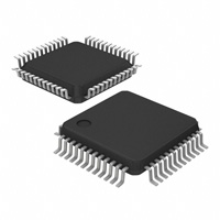


 工商网监
湘ICP备2023018690号
工商网监
湘ICP备2023018690号
