ONET1101L
www.ti.com
SLLS883 – MARCH 2008
11.3 Gbps Laser Diode Driver
FEATURES
1
•
•
•
•
•
•
•
•
•
•
Up to 11.3 Gbps Operation
Two-Wire Digital Interface
Digitally Selectable Modulation Current up to
80 mA
Digitally Selectable Bias Current up to 100 mA
Source or Sink
Automatic Power Control (APC) Loop
Supports Transceiver Management System
(TMS)
Programmable Input Equalizer
Cross-point Control
Includes Laser Safety Features
Adjustable Coupling Ratio
•
•
•
Single +3.3 V Supply
Case Temperature –25°C to 100°C
Small Surface Mount Footprint 4mm × 4mm
24-Pin, RoHS-compliant QFN Package
APPLICATIONS
•
•
•
•
•
10 Gigabit Ethernet Optical Transmitters
8x and 10x Fibre Channel Optical Transmitters
SONET OC-192/SDH STM-64 Optical
Transmitters
XFP and SFP+ Transceiver Modules
XENPAK, XPAK, X2 and 300-pin MSA
Transponder Modules
DESCRIPTION
The ONET1101L is a high-speed, 3.3 -V laser driver designed to directly modulate a laser at data rates from
2 Gbps to 11.3 Gbps.
The device provides a two-wire serial interface that helps digital control of the modulation, plus bias currents and
cross point, eliminating the need for external components. An optional input equalizer can be used for
equalization of up to 300 mm (12”) of microstrip or stripline transmission line on FR4 printed circuit boards.
The ONET1101L includes an integrated automatic power control (APC) loop, plus circuitry to support laser safety
and transceiver management systems.
The laser driver is characterized for operation from –25°C to 100°C case temperature and is available in a small
footprint using a 4mm × 4mm, 24-pin RoHS-compliant QFN package.
1
Please be aware that an important notice concerning availability, standard warranty, and use in critical applications of
Texas Instruments semiconductor products and disclaimers thereto appears at the end of this data sheet.
PRODUCTION DATA information is current as of publication date.
Products conform to specifications per the terms of the Texas
Instruments standard warranty. Production processing does not
necessarily include testing of all parameters.
Copyright © 2008, Texas Instruments Incorporated
�ONET1101L
www.ti.com
SLLS883 – MARCH 2008
These devices have limited built-in ESD protection. The leads should be shorted together or the device placed in conductive foam
during storage or handling to prevent electrostatic damage to the MOS gates.
BLOCK DIAGRAM
Figure 1 shows a block diagram of the ONET1101L device. The laser driver consists of an equalizer, a limiter, an
output driver, DC offset cancellation with cross point control, power-on reset circuitry, a 2-wire serial interface
(including a control logic block and modulation current generator), a bias current generator and automatic power
control loop, and an analog reference block.
CP Adjust
DC Offset Cancellation
Equalizer
Output Driver
MOD+
+
DIN+
100 W
MOD–
+
DIN–
Boost
Limiter
Adjustable
Boost
SDA
SDA
SCK
SCK
DIS
DIS
8 Bit Register
Settings
4 Bit Register
Settings
10 Bit Register
IMOD
10 Bit Register
IBIAS
8 Bit Register
Equalizer
7 Bit + Sign
CP Adjust
3 Bit + Sign
Limiter Current
1 Bit
CP Adjust
HC Enable
2-Wire Interface and Control Logic
BIAS
Bias
MONB
Current MONP
Generator
FLT
and
PD
APC
COMP
Power-On
Reset
Band-Gap
and
Analog
References
RZTC
BIAS
MONB
MONP
FLT
PD
COMP
RZTC
B0285-01
Figure 1. Block Diagram of the ONET1101L
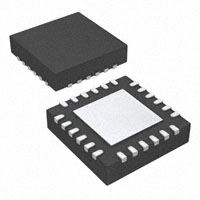
PACKAGE
The ONET1101L is packaged in a small footprint 4mm × 4mm 24-pin, RoHS-compliant QFN package, with a
lead pitch of 0.5 mm. The 24-pin QFN Package top view and pin description follow.
2
Submit Documentation Feedback
Copyright © 2008, Texas Instruments Incorporated
Product Folder Link(s) :ONET1101L
�ONET1101L
www.ti.com
SLLS883 – MARCH 2008
VCC
MOD–
MOD–
MOD+
MOD+
VCC
24
23
22
21
20
19
RGE Package
(Top View)
PD
1
18
BIAS
GND
2
17
GND
VCC
3
16
VCC
EP
12
MONB
RZTC
13
11
6
GND
SDA
10
MONP
DIN–
14
9
5
DIN+
SCK
8
COMP
GND
15
7
4
FLT
DIS
P0024-07
24-Pin QFN Package, 4mm × 4mm (Top View)
PIN DESCRIPTION
PIN
1
NAME
TYPE
PD
Analog
Photodiode input. Pin can source or sink current dependent on register setting.
Supply
Circuit ground. Exposed die pad (EP) must be grounded.
2, 8, 11, 17, EP GND
DESCRIPTION
3, 16, 19, 24
VCC
Supply
3.3 V ± 10% supply voltage
4
DIS
Digital-in
Disables the bias and modulation currents when set to high state. Toggle to reset a fault
condition.
5
SCK
Digital-in
2-wire interface serial clock. Connect a pull-up resistor (10 kΩ typical) to VCC.
6
SDA
Digital-in
2-wire interface serial data input. Connect a pull-up resistor (10 kΩ typical) to VCC.
7
FLT
Digital-out
Fault detection flag.
9
DIN+
Analog-in
Non-inverted data input. On-chip differentially 100 Ω terminated to DIN–. Must be AC
coupled.
10
DIN–
Analog-in
Inverted data input. On-chip differentially 100 Ω terminated to DIN+. Must be AC coupled.
12
RZTC
Analog
Connect external zero TC 28.7 kΩ resistor to ground (GND). Used to generate a defined
zero TC reference current for internal DACs.
13
MONB
Analog-out
Bias current monitor. Supplies a 1% replica of the bias current. Connect an external resistor
to ground (GND). If the voltage at this pin exceeds 1.16 V, a fault is triggered. Choose a
resistor that yields a MONB voltage of 0.8 V at the maximum desired bias current.
14
MONP
Analog-out
Photodiode current monitor. Supplies a 12.5% replica of the photodiode current when
PDRNG = 1X, a 25% replica when PDRNG = 01 and a 50% replica when PDRNG = 00.
Connect an external resistor (5 kΩ typical) to ground (GND).
15
COMP
Analog
Compensation pin used to control the bandwidth of the automatic power control (APC) loop.
Connect a 0.01 µF capacitor to ground.
18
BIAS
Analog
Sinks or sources average bias current for laser in both APC and open loop modes.
20, 21
MOD+
CML-out
Non-inverted modulation current output. IMOD flows into this pin when input data is high
(current).
22, 23
MOD–
CML-out
Inverted modulation current output. IMOD flows into this pin when input data is low (current).
Submit Documentation Feedback
Copyright © 2008, Texas Instruments Incorporated
Product Folder Link(s) :ONET1101L
3
�ONET1101L
www.ti.com
SLLS883 – MARCH 2008
ABSOLUTE MAXIMUM RATINGS (1)
over operating free-air temperature range (unless otherwise noted)
VALUE
UNIT
VCC
Supply voltage (2)
–0.3 to 4.0
V
VDIS, VRZTC, VSCK, VSDA, VFLT,
VMONB, VMONP, VCOMP, VPD, VBIAS
Voltage at DIS, RZTC, SCK, SDA, DIN+, DIN–, FLT,
MONB, MONP, COMP, PD, BIAS, MOD+, MOD– (2)
–0.3 to 4.0
V
IDIN–, IDIN+
Maximum current at input pins
25
mA
IMOD+, IMOD–
Maximum current at output pins
120
mA
ESD
ESD rating at all pins
TJ,max
Maximum junction temperature
TSTG
TC
(1)
(2)
2
kV (HBM)
125
°C
Storage temperature range
–65 to 150
°C
Case Temperature
–40 to 110
°C
Stresses beyond those listed under absolute maximum ratings may cause permanent damage to the device. These are stress ratings
only, and functional operation of the device at these or any other conditions beyond those indicated under recommended operating
conditions is not implied. Device exposure to conditions outside the Absolute Maximum Ratings ranges for an extended duration can
affect device reliability.
All voltage values are with respect to network ground terminal.
RECOMMENDED OPERATING CONDITIONS
over operating free-air temperature range (unless otherwise noted)
VCC
Supply voltage
VIH
Digital input high voltage
DIS, SCK, SDA
VIL
Digital input low voltage
DIS, SCK, SDA
Photodiode current range
MIN
NOM
MAX
UNIT
2.97
3.3
3.63
V
2.0
0.8
Control bit PDRNG = 1X, step size = 3 µA
3080
Control bit PDRNG = 01, step size = 1.5 µA
1540
Control bit PDRNG = 00, step size = 0.75 µA
770
RRZTC
Zero TC resistor value (1)
1.16 V bandgap bias across resistor, E96, 1% accuracy
28.4
VIN
Differential input voltage swing
EQENA = 0
100
tR-IN
Input rise time
20% to 80%
tF-IN
Input fall time
20% to 80%
TC
Case Temperature
(1)
4
V
28.7
30
–25
µA
29
1200
30
V
55
kΩ
mVp-p
ps
55
ps
100
°C
Changing the value alters the DAC ranges.
Submit Documentation Feedback
Copyright © 2008, Texas Instruments Incorporated
Product Folder Link(s) :ONET1101L
�ONET1101L
www.ti.com
SLLS883 – MARCH 2008
DC ELECTRICAL CHARACTERISTICS
Over recommended operating conditions with a 25 Ω output load, open loop operation, IMOD = 40 mA, IBIAS = 40 mA, and
RRZTC = 28.7 kΩ (unless otherwise noted)
PARAMETER
VCC
TEST CONDITIONS
MIN
TYP
MAX
UNIT
2.97
3.3
3.63
V
IMOD = 40 mA, IBIAS= 40 mA, excluding IMOD and
IBIAS, EQENA = 0
66
85
IMOD = 80 mA, IBIAS = 80 mA, excluding IMOD and
IBIAS, EQENA = 0
95
118
IMOD = 40 mA, IBIAS = 40 mA, excluding IMOD and
IBIAS, EQENA = 1
73
95
Supply voltage
IVCC
Supply current
Output off (DIS = HIGH), IMOD = 40 mA,
IBIAS = 40 mA, EQENA = 0
RIN
Data input resistance
Digital input current
120
Ω
SCK, SDA, pull up to VCC
–10
10
µA
DIS, pull down to GND
–10
10
µA
2.4
Digital output high voltage
FLT, pull-up to VCC, ISOURCE = 50 µA
VOL
Digital output low voltage
FLT, pull-up to VCC, ISINK = 350 µA
IBIAS-MIN
Minimum bias current
See table note
IBIAS-DIS
Maximum bias current
80
100
V
0.4
(1)
5
Sink, BIASPOL = 0
DAC set to maximum, open and closed loop
85
100
Source, BIASPOL = 1
DAC set to maximum, open and closed loop
80
100
BIASPOL = 0
0.8
Photodiode reverse bias voltage
Photodiode fault current level
Photodiode current monitor ratio
100
BIASPOL = 1
VCC–0.8
APC active, IPD = max
1.3
2.3
IMONP / IPD with control bit PDRNG = 1X
10%
12.5%
15%
IMONP / IPD with control bit PDRNG = 01
20%
25%
30%
Percent of target IPD
(2)
V
150%
IMONP / IPD with control bit PDRNG = 00
40%
50%
60%
IMONB / IBIAS (nominal 1/100 = 1%)
0.9%
1.0%
1.2%
VCC-RST
VCC reset threshold voltage
VCC voltage level which triggers power-on reset
2.5
2.8
VCC-RSTHYS
VCC reset threshold voltage
Hysteresis
VMONB-FLT
Fault voltage at MONB
Fault occurs if voltage at MONB exceeds value
(2)
µA
V
Bias current monitor ratio
(1)
V
mA
mA
Bias current during disable
Bias pin compliance voltage
VPD
42
Differential between DIN+ / DIN–
VOH
IBIAS-MAX
mA
100
1.1
1.16
V
mV
1.22
V
The bias current can be set below the specified minimum according to the corresponding register setting; however in closed loop
operation settings below the specified value the bias current can trigger a fault.
Assured by simulation over process, supply, and temperature variation.
Submit Documentation Feedback
Copyright © 2008, Texas Instruments Incorporated
Product Folder Link(s) :ONET1101L
5
�ONET1101L
www.ti.com
SLLS883 – MARCH 2008
AC ELECTRICAL CHARACTERISTICS
Over recommended operating conditions with 25 Ω output load, open loop operation, IMOD = 40 mA, IBIAS = 40 mA, and
RRZTC = 28.7 kΩ. Typical operating condition is at VCC = 3.3 V and TA = 25°C (unless otherwise noted)
PARAMETER
SDD11
Differential input return gain
SCD11
TEST CONDITIONS
MIN
0.01 GHz < f < 3.9 GHz
TYP
MAX
–16
dB
See note (1)
3.9 GHz < f < 12.1 GHz
UNIT
Differential to common mode
conversion gain
f < 8.25 GHz
–45
8.25 GHz < f < 20 GHz
–35
tR-OUT
Output rise time
20% to 80%, tR-IN < 40 ps, 25 Ω load, single-ended
25
35
ps
tF-OUT
Output fall time
20% to 80%, tF-IN < 40 ps, 25 Ω load, single-ended
25
35
ps
IMOD-MIN
Minimum modulation current
10
mA
IMOD-MAX
Maximum modulation current
AC Coupled Outputs
IMOD-STEP
Modulation current step size
10 Bit Register
DJ
Deterministic output jitter
RJ
70
APC time constant
µA
EQENA = 1, K28.5 pattern at 11.3 Gbps, maximum
equalization with 12” transmission line at the input, 400
mVpp at input to transmission line
7
10
psp-p
0.4
CAPC = 0.01 µF, IPD = 100 µA,
PD coupling ratio, CR = 40 (2)
0.8
30%
Rising edge of DIS to IBIAS ≤ 0.1 × IBIAS-NOMINAL (2)
TON
Disable negate time
Falling edge of DIS to IBIAS ≥ 0.9 × IBIAS-NOMINAL
TINIT1
Power-on to initialize
Power-on to registers ready to be loaded
TINIT2
Initialize to transmit
Register load STOP command to part ready to transmit
valid data (2)
TRESET
DIS pulse width
Time DIS must be held high to reset part (2)
TFAULT
Fault assert time
Time from fault condition to FLT high (2)
psRMS
µs
120
Transmitter disable time
(1)
(2)
mA
83
5
Cross Point Control Range
TOFF
85
EQENA = 0, K28.5 pattern at 11.3 Gbps, 100 mVpp,
600 mVpp, 1200 mVpp differential input voltage
Random output jitter
τAPC
dB
70%
0.05
5
µs
1
ms
1
10
ms
2
ms
50
µs
(2)
100
ns
Differential Return Gain given by SDD11, SDD22 = –11.6 + 13.33× log10(f÷8.25), f expressed in GHz
Assured by simulation over process, supply, and temperature variation.
DETAILED DESCRIPTION
EQUALIZER
The data signal can be applied to an input equalizer by means of the input signal pins DIN+ / DIN–, which
provide on-chip differential 100 Ω line-termination. The equalizer is enabled by setting EQENA = 1 (bit 1 of
register 0). Equalization of up to 300 mm (12") of microstrip or stripline transmission line on FR4 printed circuit
boards can be achieved. The amount of equalization is digitally controlled by the two-wire interface and control
logic block, and is dependant on the register settings EQADJ[0...7] (register 6). The equalizer can also be turned
off and bypassed by setting EQENA = 0. For details about the equalizer settings, see Table 12 - Register
Functionality.
LIMITER
By limiting the output signal of the equalizer to a fixed value, the limiter removes any overshoot after the input
equalization and provides the input signal for the output driver.
HIGH-SPEED OUTPUT DRIVER
The modulation current is sunk from the common emitter node of the limiting output driver differential pair by
means of a modulation current generator, which is digitally controlled by the 2-wire serial interface.
6
Submit Documentation Feedback
Copyright © 2008, Texas Instruments Incorporated
Product Folder Link(s) :ONET1101L
�ONET1101L
www.ti.com
SLLS883 – MARCH 2008
The collector nodes of the output stages are connected to the output pins MOD+ and MOD–. The laser diode
can be AC- or DC-coupled, depending on the required modulation current. To obtain the maximum modulation
current of 80 mA, AC coupling is required. The modulation outputs are optimized for driving a 25 Ω load.
MODULATION CURRENT GENERATOR
The modulation current generator provides the current for the current modulator described above. The circuit is
digitally controlled by the 2-wire interface block.
A 10-bit control bus, MODC[0...9] (register 2 and register 3), is used to set the desired modulation current.
The modulation current can be disabled by setting the DIS input pin high or setting ENA = 0 (bit 7 of register 0).
The modulation current is also disabled in a fault condition if the internal fault detection enable register flag
FLTEN is set (bit 3 of register 0).
DC OFFSET CANCELLATION AND CROSS POINT CONTROL
The ONET1101L has DC offset cancellation to compensate for internal offset voltages. The offset cancellation
can be disabled by setting OCDIS = 1 (bit 3 of register 1). Disabling the offset cancellation permits the output
crossing point to be adjusted from a minimum of 30% to 70% of the output eye diagram. The crossing point can
be moved toward the one level be setting CPSGN = 1 (bit 7 of register 7) and it can be moved toward the zero
level by setting CPSGN = 0. The shift percentage depends upon the register settings CPADJ[0...6] (register 7)
and the cross point adjustment range bits CPRNG[0...1] (register 1). Setting CPRNG1 = 0 and CPRNG0 = 0
results in minimum adjustment (fine) capability and setting CPRNG1 = 1 and CPRNG0 = 1 results in maximum
(coarse) adjustment capability.
BIAS CURRENT GENERATION AND APC LOOP
The bias current generation and APC loop are controlled by means of the 2-wire interface. In open loop
operation, selected with OLENA = 1 (bit 4 of register 0), the bias current is set directly by the 10-bit control word
BIASC[0...9] (register 4 and register 5). In automatic power control mode (select with OLENA = 0), the bias
current depends on the register settings BIASC[0...9] and the coupling ratio (CR) between the laser bias current
and the photodiode current. CR = IBIAS / IPD. If the photodiode anode is connected to the PD pin, set PDPOL = 1
(bit 0 of register 0) and if the photodiode cathode is connected to the PD pin, set PDPOL = 0.
Three photodiode current ranges can be selected by means of the PDRNG[1...0] bits (register 0). The
photodiode range should be chosen to keep the laser bias control DAC, BIASC[0...9], close to its range center.
This keeps the laser bias current set point resolution high. For details regarding the bias current setting in openand closed-loop mode, see Table 12.
The ONET1101L has the ability to source or sink the bias current. For the BIAS pin to act as a source set
BIASPOL = 1 (bit 2 of register 1) and for the BIAS pin to act as a sink set BIASPOL = 0.
The bias current is monitored using a current mirror with a gain value equal to 0.01 (1 %). By connecting a
resistor between MONB and GND, the bias current can be monitored as a voltage across the resistor. A low
temperature coefficient precision resistor should be used.
ANALOG REFERENCE
The ONET1101L laser driver is supplied by a single 3.3 V±10% supply voltage connected to the VCC pins. This
voltage is referenced to ground (GND).
On-chip bandgap voltage circuitry generates a reference voltage, independent of the supply voltage, from which
all other internally required voltages and bias currents are derived.
An external zero temperature coefficient resistor must be connected from the RZTC pin of the device to ground
(GND). This resistor is used to generate a precise, zero TC current, which is required as a reference current for
the on-chip DACs.
Submit Documentation Feedback
Copyright © 2008, Texas Instruments Incorporated
Product Folder Link(s) :ONET1101L
7
�ONET1101L
www.ti.com
SLLS883 – MARCH 2008
POWER-ON RESET
The ONET1101L has power-on reset circuitry that ensures all registers are reset to zero during startup. After the
power-on to initialize time (tINIT1), the internal registers are ready to load. The part is ready to transmit data after
the initialize to transmit time (tINIT2), assuming that the chip enable bit ENA is set to 1 and the disable pin DIS is
low.
The ONET1101L can be disabled using the ENA control register bit or the disable pin DIS. In both cases the
internal registers are not reset. After the disable pin DIS is set low or the enable bit ENA is set back to 1, the part
returns to its prior output settings.
2-WIRE INTERFACE AND CONTROL LOGIC
The ONET1101L uses a 2-wire serial interface for digital control. The two circuit inputs, SDA and SCK, are
driven, respectively, by the serial data and serial clock from a microprocessor, for example. For driving these
inputs, TI recommends an open drain output.
The 2-wire interface provides write access to the internal memory map to modify control registers and read
access to read out the control signals. The ONET1101L is a slave device only, which means that it cannot initiate
a transmission itself; it always relies on the availability of the SCK signal for the duration of the transmission. The
master device provides the clock signal plus the START and STOP commands. The protocol for a data
transmission is:
1. START command
2. 7-bit slave address (0001000) followed by an eighth bit which is the data direction bit (R/W). A zero indicates
a WRITE and a 1 indicates a READ.
3. 8-bit register address
4. 8-bit register data word
5. STOP command
Regarding timing, the ONET1101L is I2C compatible. A typical timing diagram, shown in Figure 2 and Figure 3,
describes a complete data transfer. Table 1 provides definitions of parameters for the Figure 2, I2C Timing
Diagram.
Bus Idle: Both SDA and SCK lines remain HIGH
Start Data Transfer: A change in the state of the SDA line, from HIGH to LOW, while the SCK line is HIGH,
defines a START condition (S). Each data transfer begins with a START condition.
Stop Data Transfer: A change in the state of the SDA line from LOW to HIGH while the SCK line is HIGH
defines a STOP condition (P). Each data transfer ends with a STOP condition; however, if the master still wishes
to communicate on the bus, it can generate a repeated START condition and address another slave without first
generating a STOP condition.
Data Transfer: Only one data byte can be transferred between a START and a STOP condition. The receiver
acknowledges the transfer of data.
Acknowledge: Each receiving device, when addressed, is obliged to generate an acknowledgment bit. The
transmitter releases the SDA line and a device that acknowledges, must pull down the SDA line during the
acknowledge clock pulse simultaneously so the SDA line is stable LOW during the HIGH period of the
acknowledge clock pulse. Set-up and hold times must be taken into account. When a slave-receiver fails to
acknowledge the slave address, the data line must be left HIGH by the slave. The master can generate a STOP
condition to prevent the transfer. If the slave-receiver does acknowledge the slave address but some time later in
the transfer cannot receive any more data bytes, the master must cancel the transfer. This is indicated by the
slave generating the not acknowledge on the first following byte. The slave leaves the data line HIGH and the
master generates the STOP condition.
8
Submit Documentation Feedback
Copyright © 2008, Texas Instruments Incorporated
Product Folder Link(s) :ONET1101L
�ONET1101L
www.ti.com
SLLS883 – MARCH 2008
SDA
tBUF
tLOW
tr
tHIGH
tf
tHDSTA
SCK
tHDSTA
tSUDAT
tHDSTA
P
tSUSTO
tSUSTA
S
S
P
T0295-01
2
Figure 2. I C Timing Diagram
Table 1. Timing Diagram Definitions
PARAMETER
MIN
MAX
UNIT
400
kHz
fSCK
SCK clock frequency
tBUF
Bus free time between START and STOP conditions
1.3
µs
tHDSTA
Hold time after repeated START condition. After this period, the first clock pulse is generated
0.6
µs
tLOW
Low period of the SCK clock
1.3
µs
tHIGH
High period of the SCK clock
0.6
µs
tSUSTA
Setup time for a repeated START condition
0.6
µs
tHDDAT
Data HOLD time
0
µs
tSUDAT
Data setup time
tR
Rise time of both SDA and SCK signals
300
ns
tF
Fall time of both SDA and SCK signals
300
ns
tSUSTO
Setup time for STOP condition
100
ns
µs
0.6
SDA
SCK
S
1–7
8
9
SLAVE
ADDRESS
R/W
ACK
8
1–7
9
REGISTER
ADDRESS
8
1–7
REGISTER
FUNCTION
ACK
9
P
ACK
T0296-01
2
Figure 3. I C Data Transfer
REGISTER MAPPING
The register mapping for register addresses 0 (0x00) through 9 (0x09) are shown in Table 2 through Table 11.
Table 12 describes the circuit functionality based on the register settings.
Table 2. Register 0 (0x00) Mapping – Control Settings
register address 0 (0x00)
bit 7
bit 6
bit 5
bit4
bit 3
bit 2
bit 1
bit 0
ENA
PDRNG1
PDRNG0
OLENA
FLTEN
POL
EQENA
PDPOL
Submit Documentation Feedback
Copyright © 2008, Texas Instruments Incorporated
Product Folder Link(s) :ONET1101L
9
�ONET1101L
www.ti.com
SLLS883 – MARCH 2008
Table 3. Register 1 (0x01) Mapping – Control Settings
register address 1 (0x01)
bit 7
bit 6
bit 5
bit4
bit 3
bit 2
bit 1
bit 0
–
–
–
–
OCDIS
BIASPOL
CPRNG1
CPRNG0
Table 4. Register 2 (0x02) Mapping – Modulation Current
register address 2 (0x02)
bit 7
bit 6
bit 5
bit4
bit 3
bit 2
bit 1
bit 0
–
–
–
–
–
–
MODC1
MODC0
Table 5. Register 3 (0x03) Mapping – Modulation Current
register address 3 (0x03)
bit 7
bit 6
bit 5
bit4
bit 3
bit 2
bit 1
bit 0
MODC9
MODC8
MODC7
MODC6
MODC5
MODC4
MODC3
MODC2
Table 6. Register 4 (0x04) Mapping – Bias Current
register address 4 (0x04)
bit 7
bit 6
bit 5
bit4
bit 3
bit 2
bit 1
bit 0
–
–
–
–
–
–
BIASC1
BIASC0
Table 7. Register 5 (0x05) Mapping – Bias Current
register address 5 (0x05)
bit 7
bit 6
bit 5
bit4
bit 3
bit 2
bit 1
bit 0
BIASC9
BIASC8
BIASC7
BIASC6
BIASC5
BIASC4
BIASC3
BIASC2
Table 8. Register 6 (0x06) Mapping – Equalizer Adjust
register address 6 (0x06)
bit 7
bit 6
bit 5
bit4
bit 3
bit 2
bit 1
bit 0
EQADJ7
EQADJ6
EQADJ5
EQADJ4
EQADJ3
EQADJ2
EQADJ1
EQADJ0
Table 9. Register 7 (0x07) Mapping – Cross Point Adjust
register address 7 (0x07)
bit 7
bit 6
bit 5
bit4
bit 3
bit 2
bit 1
bit 0
CPSGN
CPADJ6
CPADJ5
CPADJ4
CPADJ3
CPADJ2
CPADJ1
CPADJ0
Table 10. Register 8 (0x08) Mapping – Limiter Bias Current Adjust
register address 8 (0x08)
bit 7
bit 6
bit 5
bit4
bit 3
bit 2
bit 1
bit 0
–
–
–
–
LIMCSGN
LIMC2
LIMC1
LIMC0
Table 11. Register 9 (0x09) Mapping – High Current Enable
register address 9 (0x09)
10
bit 7
bit 6
bit 5
bit4
bit 3
bit 2
bit 1
bit 0
–
–
–
–
–
–
–
HMCENA
Submit Documentation Feedback
Copyright © 2008, Texas Instruments Incorporated
Product Folder Link(s) :ONET1101L
�ONET1101L
www.ti.com
SLLS883 – MARCH 2008
Table 12. Register Functionality
SYMBOL
REGISTER BIT
FUNCTION
ENA
Enable bit 7
Enable chip bit
1 = chip enabled. Can be toggled low to reset a fault condition.
0 = chip disabled
PDRNG1
PDRNG0
Photodiode current range bit 6
Photodiode current range bit 5
Photodiode current range bits
1X: up to 3080 µA / 3 µA resolution
01: up to 1540 µA / 1.5 µA resolution
00: up to 770 µA / 0.75 µA resolution
OLENA
Open loop enable bit 4
Open loop enable bit
1 = open loop bias current control
0 = closed loop bias current control
FLTEN
Fault detection enable bit 3
Fault detection enable bit
1 = fault detection on
0 = fault detection off
POL
Output polarity switch bit 2
Output polarity switch bit
1: pins 20 and 21 = MOD– and pins 22 and 23 = MOD+
0: pins 20 and 21 = MOD+ and pins 22 and 23 = MOD–
EQENA
Equalizer enable bit 1
Equalizer enable bit
1 = equalizer enabled
0 = equalizer disabled
PDPOL
Photodiode polarity bit 0
Photodiode polarity bit
1 = photodiode cathode connected to VCC
0 = photodiode anode connected to GND
OCDIS
Offset cancellation disable bit 3
Offset cancellation disable bit
1 = DC offset cancellation is disabled and cross point adjust is enabled
0 = DC offset cancellation is enabled and cross point adjust is disabled
BIASPOL
Bias current polarity bit 2
Bias current polarity bit
1 = Bias pin sources current
0 = Bias pin sinks current
CPRNG1
CPRNG0
Cross point range bit 1
Cross point range bit 0
Cross point adjustment range bits:
Minimum adjustment range for 00
Maximum adjustment range for 11
MODC9
Modulation current bit 9 (MSB)
Modulation current setting
MODC8
Modulation current bit 8
MODC7
Modulation current bit 7
MODC6
Modulation current bit 6
MODC5
Modulation current bit 5
MODC4
Modulation current bit 4
MODC3
Modulation current bit 3
MODC2
Modulation current bit 2
MODC1
Modulation current bit 1
MODC0
Modulation current bit 0 (LSB)
BIASC9
Bias current bit 9 (MSB)
Closed loop (APC)
BIASC8
Bias current bit 8
Coupling ratio CR = IBIAS / IPD, BIASC = 0...1023, IBIAS ≤ 100 mA
BIASC7
Bias current bit 7
BIASC6
Bias current bit 6
PDRNG = 00 (see Photodiode current range bits); IBIAS = 0.75 µA × CR × BIASC
BIASC5
Bias current bit 5
PDRNG = 01 (see Photodiode current range bits); IBIAS = 1.5 µA × CR × BIASC
BIASC4
Bias current bit 4
PDRNG = 1X (see Photodiode current range bits); IBIAS = 3 µA × CR × BIASC
BIASC3
Bias current bit 3
BIASC2
Bias current bit 2
Open loop
BIASC1
Bias current bit 1
IBIAS = 98 µA × BIASC
BIASC0
Bias current bit 0 (LSB)
Modulation current: 85 mA / 83 µA steps
Submit Documentation Feedback
Copyright © 2008, Texas Instruments Incorporated
Product Folder Link(s) :ONET1101L
11
�ONET1101L
www.ti.com
SLLS883 – MARCH 2008
Table 12. Register Functionality (continued)
SYMBOL
REGISTER BIT
FUNCTION
EQADJ7
Equalizer adjustment bit 7 (MSB)
Equalizer adjustment setting
EQADJ6
Equalizer adjustment bit 6
EQADJ5
Equalizer adjustment bit 5
EQENA = 0 (see Equalizer Enable Bit)
EQADJ4
Equalizer adjustment bit 4
Equalizer is turned off and bypassed
EQADJ3
Equalizer adjustment bit 3
EQADJ2
Equalizer adjustment bit 2
EQENA = 1 (see Equalizer Enable Bit)
EQADJ1
Equalizer adjustment bit 1
Maximum equalization for 00000000
EQADJ0
Equalizer adjustment bit 0 (LSB)
Minimum equalization for 11111111
CPSGN
Eye crossing sign bit 7
Eye cross-point adjustment setting
CPADJ6
Eye crossing adjustment bit 6 (MSB)
CPSGN = 1 (positive shift)
CPADJ5
Eye crossing adjustment bit 5
CPADJ4
Eye crossing adjustment bit 4
CPADJ3
Eye crossing adjustment bit 3
CPADJ2
Eye crossing adjustment bit 2
Maximum shift for 1111111
CPADJ1
Eye crossing adjustment bit 1
Minimum shift for 0000000
CPADJ0
Eye crossing adjustment bit 0 (LSB)
LIMCSGN
Limiter current sign bit 3
Limiter bias current setting
LIMC2
Limiter current bit 2 (MSB)
LIMCSGN = 1: decrease current
LIMC1
Limiter current bit 1
LIMCSGN = 0: increase current
LIMC0
Limiter current bit 0 (LSB)
No change for 000 and maximum change for 111
HMCENA
High modulation current enable bit 0
High modulation current enable bit
1 = high modulation current capability up to 100 mA
0 = modulation current capability up to 80 mA
Maximum shift for 1111111
Minimum shift for 0000000
CPSGN = 0 (negative shift)
LASER SAFETY FEATURES AND FAULT RECOVERY PROCEDURE
The ONET1101L provides built-in laser safety features and can detect these fault conditions:
• Voltage at MONB exceeds the voltage at RZTC (1.16 V)
• Photodiode current exceeds 150% of its set value
• Bias control DAC drops in value by more than 50% in one step
If
•
•
•
one or more fault conditions happen and the fault enable bit FLTEN is set to 1, the ONET1101L responds by:
Setting the bias current to zero.
Setting the modulation current to zero.
Asserting and latching the FLT pin.
ONET1101L Fault recovery happens using this procedure:
1. The disable pin DIS or the internal enable control bit ENA are toggled for at least the fault latch reset time.
2. The FLT pin de-asserts while the disable pin DIS is asserted or the enable bit ENA is de-asserted.
3. If the fault condition is no longer present, the part returns to normal operation with its prior output settings
after the disable negate time.
4. If the fault condition is still present, FLT re-asserts once DIS is set to a low level and the part does not return
to normal operation.
12
Submit Documentation Feedback
Copyright © 2008, Texas Instruments Incorporated
Product Folder Link(s) :ONET1101L
�ONET1101L
www.ti.com
SLLS883 – MARCH 2008
TYPICAL OPERATION CHARACTERISTICS
Typical operating condition is at VCC = 3.3 V, TA = 25°C, IBIAS = 40 mA, IMOD = 40 mA, VIN = 600 mVpp (unless otherwise
noted).
DETERMINISTIC JITTER
vs
TEMPERATURE
8
8
7
7
6
6
Deterministic Jitter − psPP
Deterministic Jitter − psPP
DETERMINISTIC JITTER
vs
MODULATION CURRENT
5
4
3
2
5
4
3
2
1
1
0
−40
0
10
20
30
40
50
60
70
80
−20
0
20
40
60
80
TA − Free-Air Temperature − °C
Modulation Current − mA
G001
Figure 4.
Figure 5.
RANDOM JITTER
vs
MODULATION CURRENT
RANDOM JITTER
vs
TEMPERATURE
100
G002
0.4
0.5
0.4
Random Jitter − psrms
Random Jitter − psrms
0.3
0.3
0.2
0.2
0.1
0.1
0.0
10
20
30
40
50
60
70
80
0.0
−40
−20
Modulation Current − mA
G003
Figure 6.
0
20
40
60
80
TA − Free-Air Temperature − °C
100
G004
Figure 7.
Submit Documentation Feedback
Copyright © 2008, Texas Instruments Incorporated
Product Folder Link(s) :ONET1101L
13
�ONET1101L
www.ti.com
SLLS883 – MARCH 2008
TYPICAL OPERATION CHARACTERISTICS (continued)
Typical operating condition is at VCC = 3.3 V, TA = 25°C, IBIAS = 40 mA, IMOD = 40 mA, VIN = 600 mVpp (unless otherwise
noted).
RISE-TIME AND FALL-TIME
vs
MODULATION CURRENT
RISE-TIME AND FALL-TIME
vs
TEMPERATURE
35
35
Rise Time
25
Fall Time
tt − Transition Time − ps
tt − Transition Time − ps
30
20
15
10
5
30
Rise Time
25
Fall Time
20
15
10
5
0
10
20
30
40
50
60
70
0
−40
80
−20
G005
20
40
80
Figure 9.
BIAS CURRENT IN OPEN LOOP MODE
vs
BIASC REGISTER SETTING
BIAS-MONITOR CURRENT IMONB
vs
BIAS CURRENT
120
1.2
100
1.0
80
60
40
20
100
G006
0.8
0.6
0.4
0.2
0.0
0
0
200
400
600
800
1000
1200
10
20
30
40
50
60
70
80
90
100
Bias Current − mA
Bias Current Register Setting − Decimal
G008
G007
Figure 10.
14
60
Figure 8.
IMONB − Bias-Monitor Current − mA
Open Loop Bias Current − mA
0
TA − Free-Air Temperature − °C
Modulation Current − mA
Figure 11.
Submit Documentation Feedback
Copyright © 2008, Texas Instruments Incorporated
Product Folder Link(s) :ONET1101L
�ONET1101L
www.ti.com
SLLS883 – MARCH 2008
TYPICAL OPERATION CHARACTERISTICS (continued)
Typical operating condition is at VCC = 3.3 V, TA = 25°C, IBIAS = 40 mA, IMOD = 40 mA, VIN = 600 mVpp (unless otherwise
noted).
PHOTODIODE-MONITOR CURRENT IMONP
vs
PD CURRENT
MODULATION CURRENT
vs
MODC REGISTER SETTING
90
0.25
0.20
70
Modulation Current − mA
Photodiode Monitor Current − mA
80
0.15
0.10
60
50
40
30
20
0.05
10
0.00
0.05 0.15 0.25
0
0.35 0.45 0.55
0.65 0.75 0.85
Photodiode Current − mA
0
200
400
600
800
1000
1200
Modulation Current Register Setting − Decimal
G009
G010
Figure 12.
Figure 13.
SUPPLY CURRENT (includes IBIAS and IMOD)
vs
TEMPERATURE
EYE-DIAGRAM AT 11.3 GBPS, PRBS-31 PATTERN
IMOD = 20 mA, EQENA = 0
200
190
Supply Current − mA
(Including IBIAS and IMOD)
180
170
160
150
140
130
120
110
100
−40
−20
0
20
40
60
80
TA − Free-Air Temperature − °C
14.8 ps / Div
100
G012
G011
Figure 14.
Figure 15.
Submit Documentation Feedback
Copyright © 2008, Texas Instruments Incorporated
Product Folder Link(s) :ONET1101L
15
�ONET1101L
www.ti.com
SLLS883 – MARCH 2008
TYPICAL OPERATION CHARACTERISTICS (continued)
Typical operating condition is at VCC = 3.3 V, TA = 25°C, IBIAS = 40 mA, IMOD = 40 mA, VIN = 600 mVpp (unless otherwise
noted).
EYE-DIAGRAM AT 11.3GBPS, PRBS-31 PATTERN
IMOD = 40 mA, EQENA = 0
EYE-DIAGRAM AT 11.3GBPS, PRBS-31 PATTERN
IMOD = 60 mA, EQENA = 0
14.5 ps / Div
14.6 ps / Div
G013
G014
Figure 16.
Figure 17.
EYE-DIAGRAM AT 11.3GBPS, PRBS-31 PATTERN
IMOD = 40 mA, EQENA = 1
12" OF FR4 AT INPUTS
14 ps / Div
G015
Figure 18.
16
Submit Documentation Feedback
Copyright © 2008, Texas Instruments Incorporated
Product Folder Link(s) :ONET1101L
�ONET1101L
www.ti.com
SLLS883 – MARCH 2008
APPLICATION INFORMATION
Figure 19 and Figure 20 show typical application circuits using the ONET1101L with a laser biased to VCC (BIAS
pin sink) and driven differentially or single-ended. The laser driver is controlled using the 2-wire interface
SDA/SCK by a microcontroller. In a typical application, the FLT, MONB, and MONP outputs are also connected
to the microcontroller for transceiver management purposes.
The component values in Figure 19 and Figure 20 are typical examples and may be varied according to the
intended application.
DIS
VCC
SDK
0.1 mF
SDA
C1
0.1 mF
MOD–
ONET1101L
GND
MOD+
BLM15HG601SN1
(See Note 1)
(See
Note
1)
(See
Note 1)
(See Note 1)
BIAS
GND
VCC
VCC
RZTC
COMP
MOD+
MONP
C2
0.1 mF
DIN–
MONB
DIN–
0.1 mF
MOD–
GND
DIN+
DIN+
BLM15HG601SN1 ´ 2
VCC
FLT
FLT
BLM15HD102SN1
PD
GND
VCC
DIS
SDA
SCK
BLM15HD102SN1 ´ 2
0.1 mF
Laser
Monitor
Photodiode
0.1 mF
BLM15HG601SN1
0.1 mF
RZTC
28.7 kW
BLM15HD102SN1
0.1 mF
1000 pF
MONB
RMONB
1.2 kW
MONP
RMONP
5 kW
CCOMP
0.01 mF
S0319-01
(1)
Resistor values depend on the TOSA diode used.
Figure 19. AC Coupled Differential Drive
Submit Documentation Feedback
Copyright © 2008, Texas Instruments Incorporated
Product Folder Link(s) :ONET1101L
17
�ONET1101L
www.ti.com
SLLS883 – MARCH 2008
DIS
VCC
SDK
0.1 mF
SDA
C1
0.1 mF
MOD+
GND
MOD+
Laser
50 W
Diff TL
25 W TL
0.1 mF
BIAS
VCC
GND
VCC
COMP
RZTC
MONP
DIN–
MONB
C2
0.1 mF
BLM15HG601SN1
0.1 mF
MOD–
ONET1101L
DIN–
0.1 mF
MOD–
GND
DIN+
DIN+
BLM15HD102SN1 ´ 2
VCC
FLT
FLT
BLM15HD102SN1
PD
GND
VCC
DIS
SDA
SCK
25 W
Monitor
Photodiode
Optional
BLM15HG601SN1
0.1 mF
RZTC
28.7 kW
BLM15HD102SN1
0.1 mF
1000 pF
MONB
RMONB
1.2 kW
MONP
CCOMP
0.01 mF
RMONP
5 kW
S0320-01
Figure 20. AC Coupled Single-Ended Drive
CALCULATING POWER CONSUMPTION
The power dissipation is different, depending if the BIAS pin is sourcing or sinking current. Lower power
dissipation in the ONET1101L can be achieved if the BIAS pin sinks the bias current because the BIAS pin
compliance voltage is typically less than 1 V.
The power dissipation is calculated as:
P = VCC × (IVCC + IMOD) + (VBIAS × IBIAS)
Where:
VCC is the power supply voltage
IVCC is the supply current excluding modulation and bias current
IMOD is the modulation current
VBIAS is the voltage at the BIAS pin
IBIAS is the bias current
18
Submit Documentation Feedback
Copyright © 2008, Texas Instruments Incorporated
Product Folder Link(s) :ONET1101L
�ONET1101L
www.ti.com
SLLS883 – MARCH 2008
LAYOUT GUIDELINES
For optimum performance, use 50 Ω transmission lines (100 Ω differential) for connecting the signal source to
the DIN+ and DIN– pins and 25 Ω transmission lines (50 Ω differential) for connecting the modulation current
outputs, MOD+ and MOD–, to the laser. The length of the transmission lines should be kept as short as possible
to reduce loss and pattern-dependent jitter. It is recommended to assemble the series matching resistor as close
as possible to the TOSA diode, if required.
Submit Documentation Feedback
Copyright © 2008, Texas Instruments Incorporated
Product Folder Link(s) :ONET1101L
19
�PACKAGE OPTION ADDENDUM
www.ti.com
14-Oct-2022
PACKAGING INFORMATION
Orderable Device
Status
(1)
Package Type Package Pins Package
Drawing
Qty
Eco Plan
(2)
Lead finish/
Ball material
MSL Peak Temp
Op Temp (°C)
Device Marking
(3)
Samples
(4/5)
(6)
ONET1101LRGER
ACTIVE
VQFN
RGE
24
3000
RoHS & Green
NIPDAU
Level-2-260C-1 YEAR
-25 to 100
ONET
1101L
Samples
ONET1101LRGET
ACTIVE
VQFN
RGE
24
250
RoHS & Green
NIPDAU
Level-2-260C-1 YEAR
-25 to 100
ONET
1101L
Samples
(1)
The marketing status values are defined as follows:
ACTIVE: Product device recommended for new designs.
LIFEBUY: TI has announced that the device will be discontinued, and a lifetime-buy period is in effect.
NRND: Not recommended for new designs. Device is in production to support existing customers, but TI does not recommend using this part in a new design.
PREVIEW: Device has been announced but is not in production. Samples may or may not be available.
OBSOLETE: TI has discontinued the production of the device.
(2)
RoHS: TI defines "RoHS" to mean semiconductor products that are compliant with the current EU RoHS requirements for all 10 RoHS substances, including the requirement that RoHS substance
do not exceed 0.1% by weight in homogeneous materials. Where designed to be soldered at high temperatures, "RoHS" products are suitable for use in specified lead-free processes. TI may
reference these types of products as "Pb-Free".
RoHS Exempt: TI defines "RoHS Exempt" to mean products that contain lead but are compliant with EU RoHS pursuant to a specific EU RoHS exemption.
Green: TI defines "Green" to mean the content of Chlorine (Cl) and Bromine (Br) based flame retardants meet JS709B low halogen requirements of


 工商网监
湘ICP备2023018690号
工商网监
湘ICP备2023018690号
