ONET1191P
www.ti.com
SLLS754 – SEPTEMBER 2006
11.3-Gbps Limiting Amplifier
FEATURES
APPLICATIONS
•
•
•
•
•
•
•
•
•
•
Up to 11.3-Gbps Operation
Loss-of-Signal Detection (LOS)
Adjustable Output Voltage
Low Power Consumption
Input Offset Cancellation
CML Data Outputs With On-Chip, 50-Ω
Back-Termination to VCC
Single 3.3 V Supply
Surface-Mount, Small-Footprint, 3-mm ×
3-mm, 16-Pin QFN Package
•
•
•
•
10 Gigabit Ethernet Optical Transmitters
8× and 10× Fibre Channel Optical
Transmitters
SONET OC-192/SDH-64 Optical Transmitters
XFP and SFP+ Transceiver Modules
XENPAK, XPAK, X2 and 300-Pin MSA
Transponder Modules
Cable Driver and Receiver
DESCRIPTION
The ONET1191P is a high-speed, 3.3-V limiting amplifier for copper-cable and fiber-optic applications with data
rates up to 11.3 Gbps.
This device provides a gain of about 40 dB which ensures a fully differential output swing for input signals as low
as 5 mVpp. The output amplitude can be adjusted from 400 mVpp to 700 mVpp. Loss-of-signal detection and
output disable are also provided.
The part is available in a small-footprint, 3-mm × 3-mm, 16-pin QFN package, typically dissipates less than 110
mW, and is characterized for operation from –40°C to 85°C.
Please be aware that an important notice concerning availability, standard warranty, and use in critical applications of Texas
Instruments semiconductor products and disclaimers thereto appears at the end of this data sheet.
PRODUCTION DATA information is current as of publication date.
Products conform to specifications per the terms of the Texas
Instruments standard warranty. Production processing does not
necessarily include testing of all parameters.
Copyright © 2006, Texas Instruments Incorporated
�ONET1191P
www.ti.com
SLLS754 – SEPTEMBER 2006
BLOCK DIAGRAM
A simplified block diagram of the ONET1191P is shown in Figure 1.
This compact, low-power, 11.3-Gbps limiting amplifier consists of a high-speed data path with offset cancellation
(dc feedback), a loss-of-signal detection block using two peak detectors, and a band-gap voltage reference and
bias current generation block.
DC Feedback Stage
COC+
+
COC–
–
50 W
50 W
Bandgap Voltage
Reference and
Bias Current Generation
12 dB
Gain Stage
20 dB
Gain Stage
8 dB
Gain Stage
DIN+
+
+
+
DOUT+
DIN–
–
–
–
DOUT–
VCC
GND
DISABLE
Peak
Detector
Peak
Detector
Loss of Signal Detection
VAR
LOS
TH
B0067-02
Figure 1. Simplified Block Diagram of the ONET1191P
HIGH-SPEED DATA PATH
The high-speed data signal is applied to the data path by means of the input signal pins, DIN+/DIN–. The data
path consists of a 12-dB input gain stage with 2 × 50-Ω on-chip line-termination resistors, a second gain stage
with 20 dB of gain, and a variable-gain output stage which provides another 8 dB of gain. The amplified data
output signal is available at the output pins DOUT+/DOUT–, which include on-chip 2 × 50-Ω back-termination to
VCC. The output amplitude can be adjusted between 400 mVpp and 700 mVpp by connecting an external resistor
between the VAR pin and ground (GND).
A dc feedback stage compensates for internal offset voltages and thus ensures proper operation even for very
small input data signals. This stage is driven by the output signal of the second gain stage. The signal is
low-pass filtered, amplified, and fed back to the input of the first gain stage via the on-chip, 50-Ω termination
resistors. The required low-frequency cutoff is determined by an external 0.1 µF capacitor, which must be
differentially connected to the COC+/COC– pins.
LOSS-OF-SIGNAL DETECTION
The peak values of the input signal and output signal of the first gain stage are monitored by two peak detectors.
The peak values are compared to a predefined loss-of-signal threshold voltage inside the loss-of-signal
detection block. As a result of the comparison, the LOS signal, which indicates that the input signal amplitude is
below the defined threshold level, is generated.
The threshold voltage can be set within a certain range by means of an external resistor connected between the
TH pin and ground.
2
Submit Documentation Feedback
�ONET1191P
www.ti.com
SLLS754 – SEPTEMBER 2006
BAND-GAP VOLTAGE AND BIAS GENERATION
The ONET1191P limiting amplifier is supplied by a single 3.3-V supply voltage connected to the VCC pins. This
voltage is referred to ground (GND).
On-chip band-gap voltage circuitry generates a reference voltage, independent of supply voltage, from which all
other internally required voltages and bias currents are derived.
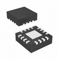
PACKAGE
For the ONET1191P, a small-footprint, 3-mm × 3-mm, 16-pin QFN package, with a lead pitch of 0,5 mm, is
used. The pinout is shown in Figure 2.
VCC
1
VCC
2
GND
DOUT+
DOUT–
GND
RGT PACKAGE
(TOP VIEW)
16
15
14
13
12
VAR
11
DISABLE
EP
GND
4
9
TH
5
6
7
8
DIN–
LOS
DIN+
10
COC+
3
COC–
GND
P0019-05
Figure 2. Pinout of ONET1191P in a 3-mm × 3-mm, 16-Pin QFN Package
TERMINAL FUNCTIONS
TERMINAL
TYPE
DESCRIPTION
6
Analog
Offset cancellation filter capacitor plus terminal. An external 0.1 µF filter capacitor must be
connected between this pin and COC– (pin 5).
COC–
5
Analog
Offset cancellation filter capacitor minus terminal. An external 0.1 µF filter capacitor must be
connected between this pin and COC+ (pin 6).
DIN+
7
Analog input
Noninverted data input. On-chip, 50-Ω terminated to COC+. Differentially 100-Ω terminated
to DIN–.
DIN–
8
Analog input
Inverted data input. On-chip, 50-Ω terminated to COC–. Differentially 100-Ω terminated to
DIN+.
DISABLE
11
CMOS input
Disables the output stage when set to a high level
DOUT+
15
CML out
Noninverted data output. On-chip, 50-Ω back-terminated to VCC.
DOUT–
14
CML out
Inverted data output. On-chip, 50-Ω back-terminated to VCC.
GND
3, 4, 13, 16,
EP
Supply
LOS
10
Open-drain
MOS
High level indicates that the input signal amplitude is below the programmed threshold level.
Open-drain output. Requires an external 10-kΩ pullup resistor to VCC for proper operation.
TH
9
Analog input
LOS threshold adjustment with resistor to GND
VAR
12
Analog input
Variable output amplitude control. Output amplitude can be reduced to 400 mVpp by
grounding the VAR pin. Output amplitude can be set from 400 mVpp to 700 mVpp by
connecting a 0 to 100-kΩ resistor to GND or leaving the pin open.
VCC
1, 2
Supply
NAME
NO.
COC+
Circuit ground. Exposed die pad (EP) must be grounded.
3.3-V ±10% supply voltage
Submit Documentation Feedback
3
�ONET1191P
www.ti.com
SLLS754 – SEPTEMBER 2006
ABSOLUTE MAXIMUM RATINGS
over operating free-air temperature range (unless otherwise noted) (1)
VALUE
UNIT
VCC
Supply voltage (2)
–0.3 to 4
V
VDIN+, VDIN–
Voltage at DIN+, DIN– (2)
0.5 to 4
V
–0.3 to 4
V
±1.25
V
mA
DOUT– (2)
VLOS, VCOC+, VCOC–, VTH, VDOUT+,
VDOUT–
Voltage at LOS, COC+, COC–, TH, DOUT+,
VDIN,DIFF
Differential voltage between DIN+ and DIN–
ILOS
Current into LOS
1
IDIN+, IDIN–, IDOUT+, IDOUT–
Continuous current at inputs and outputs
20
mA
ESD
ESD rating at all pins
1.5
kV (HBM)
TJ,max
Maximum junction temperature
125
°C
TSTG
Storage temperature range
–65 to 85
°C
TA
Characterized free-air operating temperature range
–40 to 85
°C
TLEAD
Lead temperature 1,6 mm (1/16 inch) from case for 10 seconds
260
°C
(1)
(2)
Stresses beyond those listed under absolute maximum ratings may cause permanent damage to the device. These are stress ratings
only, and functional operation of the device at these or any other conditions beyond those indicated under recommended operating
conditions is not implied. Exposure to absolute-maximum-rated conditions for extended periods may affect device reliability.
All voltage values are with respect to network ground terminal.
RECOMMENDED OPERATING CONDITIONS
MIN
TYP
MAX
VCC
Supply voltage
2.9
3.3
3.6
V
TA
Operating free-air temperature
–40
85
°C
Disable input high voltage
2
V
Disable input low voltage
0.25
Optimum LOS threshold resistor
RVAR range
UNIT
V
32
62
kΩ
0
open
kΩ
DC ELECTRICAL CHARACTERISTICS
over recommended operating conditions, outputs connected to a 50-Ω load, RVAR = open (unless otherwise noted)
PARAMETER
MIN
TYP
MAX
2.9
3.3
3.6
V
DISABLE = LOW
33
49
mA
Data input resistance
Single-ended to COC pins
50
Ω
Data output resistance
Single-ended, referenced to VCC
50
Ω
1.25
V
VCC
Supply voltage
IVCC
Supply current
RIN
ROUT
TEST CONDITIONS
Voltage at TH pin
4
LOS HIGH voltage
10-kΩ pullup to VCC, ISOURCE = 50 µA
LOS LOW voltage
10-kΩ pullup to VCC, ISINK = 200 µA
Submit Documentation Feedback
UNIT
2.4
0.5
V
�ONET1191P
www.ti.com
SLLS754 – SEPTEMBER 2006
AC ELECTRICAL CHARACTERISTICS
over recommended operating conditions, outputs connected to a 50-Ω load, RVAR = open (unless otherwise noted). Typical
operating condition is at VCC = 3.3 V and TA = 25°C.
PARAMETER
f3dB-H
High-frequency –3-dB bandwidth
f3dB-L
Low-frequency –3-dB bandwidth
vIN,MIN
Data input sensitivity
A
Small-signal gain
VIN,MAX
Data input overload
DJ
Deterministic jitter
RJ
Random jitter
VOD
Differential data output voltage
tr
tf
VTH
TEST CONDITIONS
MIN
TYP
MAX
UNIT
8
11
15
GHz
COC = 0.1 µF, ac coupling capacitors = 0.1 µF
30
K28.5 at 11.3 Gbps, BER < 10–12
2.5
5
VOD-min ≥ 0.95 × VOD (output limited)
10
20
40
44
34
kHz
2000
4
7
VIN = 20 mVpp, K28.5 at 11.3 Gbps
4
9
Input = 5 mVpp
1.6
Input = 20 mVpp
0.7
pspp
psRMS
700
900
DISABLE = HIGH
25
100
Output rise time
20% to 80%, VIN ≥ 20 mVPP
25
35
ps
Output fall time
20% to 80%, VIN ≥ 20 mVPP
25
35
ps
K28.5 pattern at 10.7 Gbps, RTH = 62 kΩ
40
K28.5 pattern at 10.7 Gbps, RTH = 32 kΩ
65
LOS assert threshold range
LOS threshold variation
LOS hysteresis
tLOS_AST
LOS assert time
tLOS, DEA_
LOS deassert time
tDIS
Disable response time
600
dB
mVpp
VIN = 5 mVpp, K28.5 at 11.3 Gbps
VIN ≥ 20 mVpp, DISABLE = LOW
mVpp
Versus temperature
3
Versus supply voltage VCC
1
K28.5 pattern at 11.3 Gbps
1.5
1300
Submit Documentation Feedback
mVpp
mVpp
dB
dB
7
dB
2000
ns
120
ns
90
ns
5
�ONET1191P
www.ti.com
SLLS754 – SEPTEMBER 2006
TYPICAL OPERATION CHARACTERISTICS
Typical operating condition is at VCC = 3.3 V, TA = 25°C, and RVAR = open (unless otherwise noted)
FREQUENCY RESPONSE
TRANSFER FUNCTION
800
50
VOD − Differential Output Voltage − mVpp
45
SDD21 − Gain − dB
40
35
30
25
20
15
10
5
0
0.1
700
600
500
400
300
200
100
0
1
10
0
100
G001
DIFFERENTIAL INPUT RETURN GAIN
vs
FREQUENCY
DIFFERENTIAL OUTPUT RETURN GAIN
vs
FREQUENCY
20
G002
0
−5
−10
−15
−20
−25
−30
1
10
100
−5
−10
−15
−20
−25
−30
−35
0.1
1
10
100
f − Frequency − GHz
f − Frequency − GHz
G004
G003
Figure 5.
6
15
Figure 4.
SDD22 − Differential Output Return Gain − dB
SDD11 − Differential Input Return Gain − dB
10
Figure 3.
0
−35
0.1
5
VID − Differential Input Voltage − mVpp
f − Frequency − GHz
Figure 6.
Submit Documentation Feedback
�ONET1191P
www.ti.com
SLLS754 – SEPTEMBER 2006
TYPICAL OPERATION CHARACTERISTICS (continued)
Typical operating condition is at VCC = 3.3 V, TA = 25°C, and RVAR = open (unless otherwise noted)
BIT-ERROR RATIO
vs
INPUT AMPLITUDE (11.3 GBPS)
DETERMINISTIC JITTER
vs
INPUT AMPLITUDE
100
10
10-3
9
8
Deterministic Jitter − ps
10-6
Bit-Error Ratio
10-9
10-12
10-15
10-18
6
5
4
3
10-21
2
10-24
1
0
10-27
0
1
2
3
0
4
VID − Differential Input Voltage − mVpp
400
800
1200
1600
VID − Differential Input Voltage − mVpp
G005
Figure 7.
Figure 8.
RANDOM JITTER
vs
INPUT AMPLITUDE
LOS ASSERT/DEASSERT VOLTAGE
vs
THRESHOLD RESISTANCE
2.0
2000
G006
400
LOS Assert/Deassert Voltage − mVpp
1.8
1.6
Random Output Jitter − ps
7
1.4
1.2
1.0
0.8
0.6
0.4
0.2
350
300
250
LOS Deassert Voltage
200
150
100
50
LOS Assert Voltage
0.0
0
0
10
20
30
40
50
60
70
80
VID − Differential Input Voltage − mVpp
90 100
0
10
G007
Figure 9.
20
30
40
50
60
70
80
RTH − Threshold Resistance − kΩ
90 100
G008
Figure 10.
Submit Documentation Feedback
7
�ONET1191P
www.ti.com
SLLS754 – SEPTEMBER 2006
TYPICAL OPERATION CHARACTERISTICS (continued)
Typical operating condition is at VCC = 3.3 V, TA = 25°C, and RVAR = open (unless otherwise noted)
LOS HYSTERESIS
vs
THRESHOLD RESISTANCE
OUTPUT AMPLITUDE
vs
RVAR
800
VID − Differential Output Voltage − mVpp
6
LOS Hysteresis − dB
5
4
3
2
1
700
600
500
400
300
200
100
0
0
0
10
20
30
40
50
60
70
80
90 100
RTH − Threshold Resistance − kΩ
0
10
20
30
40
50
60
80
90 100
RVAR − Variable Resistance − kΩ
G009
G010
Figure 11.
Figure 12.
OUTPUT EYE-DIAGRAM AT 10.3 GBPS
AND MINIMUM INPUT VOLTAGE (5 mVpp)
OUTPUT EYE-DIAGRAM AT 10.3 GBPS
AND MAXIMUM INPUT VOLTAGE (2000 mVpp)
100 mV/ Div
100 mV/ Div
15 ps / Div
15 ps / Div
G012
G011
Figure 13.
8
70
Figure 14.
Submit Documentation Feedback
�ONET1191P
www.ti.com
SLLS754 – SEPTEMBER 2006
TYPICAL OPERATION CHARACTERISTICS (continued)
Typical operating condition is at VCC = 3.3 V, TA = 25°C, and RVAR = open (unless otherwise noted)
OUTPUT EYE-DIAGRAM AT 8.5 GBPS
AND MINIMUM INPUT VOLTAGE (5 mVpp)
100 mV/ Div
OUTPUT EYE-DIAGRAM AT 8.5 GBPS
AND MAXIMUM INPUT VOLTAGE (2000 mVpp)
100 mV/ Div
20 ps / Div
20 ps / Div
G014
G013
Figure 15.
Figure 16.
Submit Documentation Feedback
9
�ONET1191P
www.ti.com
SLLS754 – SEPTEMBER 2006
APPLICATION INFORMATION
Figure 17 shows a typical application circuit using the ONET1191P. The output amplitude can be adjusted with
RVAR and the LOS assert voltage is adjusted with RTH.
L1
BLM11HA102SG
VCC
COC+
DIN+
DIN+
DIN–
VCC
VCC
ONET1191P
16-Pin QFN
TH
C2
0.1 mF
LOS
DIN–
C3
0.1 mF
DOUT+
DOUT+
DOUT–
DOUT–
GND
C4
0.1 mF
VAR
C1
0.1 mF
GND
COC–
DISABLE
C5
0.1 mF
GND
GND
C6
0.1 mF
DISABLE
LOS
RTH
12 kW – 62 kW
R1
10 kW
RVAR
0 W – Open
GND
S0099-03
Figure 17. Basic Application Circuit
10
Submit Documentation Feedback
�PACKAGE OPTION ADDENDUM
www.ti.com
14-Oct-2022
PACKAGING INFORMATION
Orderable Device
Status
(1)
Package Type Package Pins Package
Drawing
Qty
Eco Plan
(2)
Lead finish/
Ball material
MSL Peak Temp
Op Temp (°C)
Device Marking
(3)
Samples
(4/5)
(6)
ONET1191PRGTR
ACTIVE
VQFN
RGT
16
3000
RoHS & Green
NIPDAU
Level-2-260C-1 YEAR
-40 to 85
191P
Samples
ONET1191PRGTT
ACTIVE
VQFN
RGT
16
250
RoHS & Green
NIPDAU
Level-2-260C-1 YEAR
-40 to 85
191P
Samples
(1)
The marketing status values are defined as follows:
ACTIVE: Product device recommended for new designs.
LIFEBUY: TI has announced that the device will be discontinued, and a lifetime-buy period is in effect.
NRND: Not recommended for new designs. Device is in production to support existing customers, but TI does not recommend using this part in a new design.
PREVIEW: Device has been announced but is not in production. Samples may or may not be available.
OBSOLETE: TI has discontinued the production of the device.
(2)
RoHS: TI defines "RoHS" to mean semiconductor products that are compliant with the current EU RoHS requirements for all 10 RoHS substances, including the requirement that RoHS substance
do not exceed 0.1% by weight in homogeneous materials. Where designed to be soldered at high temperatures, "RoHS" products are suitable for use in specified lead-free processes. TI may
reference these types of products as "Pb-Free".
RoHS Exempt: TI defines "RoHS Exempt" to mean products that contain lead but are compliant with EU RoHS pursuant to a specific EU RoHS exemption.
Green: TI defines "Green" to mean the content of Chlorine (Cl) and Bromine (Br) based flame retardants meet JS709B low halogen requirements of


 工商网监
湘ICP备2023018690号
工商网监
湘ICP备2023018690号
