ONET4291PA
www.ti.com
SLLS671 – SEPTEMBER 2005
1-Gbps to 4.25-Gbps Rate-Selectable Limiting Amplifier
FEATURES
•
•
•
•
•
•
•
•
Multirate Operation from 1 Gbps up to
4.25 Gbps
Loss-of-Signal Detection (LOS)
Two-Wire Digital Interface
Digitally Selectable LOS Threshold
Digitally Selectable Bandwidth
Digitally Selectable Output Voltage
Low Power Consumption
Input Offset Cancellation
•
•
•
CML Data Outputs With On-Chip, 50-Ω
Back-Termination to VCC
Single 3.3-V Supply
Surface-Mount, Small-Footprint, 4-mm ×
4-mm, 16-Terminal QFN Package
APPLICATIONS
•
•
•
Multirate SONET/SDH Transmission Systems
4.25-Gbps, 2.125-Gbps, and 1.0625-Gbps
Fibre-Channel Receivers
Gigabit Ethernet Receivers
DESCRIPTION
The ONET4291PA is a versatile, high-speed, rate-selectable limiting amplifier for multiple fiber-optic applications
with data rates up to 4.25 Gbps.
The device provides a two-wire interface, which allows digital bandwidth selection, digital output amplitude
selection, and digital loss of signal threshold adjust.
This device provides a gain of about 43 dB, which ensures a fully differential output swing for input signals as low
as 5 mVp-p.
The ONET4291PA provides loss-of-signal detection with either digital or analog threshold adjust.
The part is available in a small-footprint, 4-mm × 4-mm, 16-terminal QFN package. It requires a single 3.3-V
supply.
This power-efficient, rate-selectable limiting amplifier is characterized for operation from –40°C to 85°C ambient
temperature.
Please be aware that an important notice concerning availability, standard warranty, and use in critical applications of Texas
Instruments semiconductor products and disclaimers thereto appears at the end of this data sheet.
PRODUCTION DATA information is current as of publication date.
Products conform to specifications per the terms of the Texas
Instruments standard warranty. Production processing does not
necessarily include testing of all parameters.
Copyright © 2005, Texas Instruments Incorporated
�ONET4291PA
www.ti.com
SLLS671 – SEPTEMBER 2005
BLOCK DIAGRAM
A simplified block diagram of the ONET4291PA is shown in Figure 1.
This compact, 3.3-V, low-power, 1-Gbps to 4.25-Gbps rate-selectable limiting amplifier consists of a high-speed
data path with offset cancellation block (dc feedback), a loss-of-signal detection block using two peak detectors,
a programmable resistor, a two-wire interface and control-logic block, and a band-gap voltage reference and
bias-current generation block.
DC Feedback Stage
COC+
+
COC−
−
50 Ω
Band-Gap Voltage
Reference and
Bias Current Generation
50 Ω
CML Output Buffer
DIN+
DIN−
Bandwidth
Switch
+
+
+
DOUT+
−
−
−
DOUT−
Gain Stage
VCC
4
Gain Stage
Peak
Detector
GND
Peak
Detector
2
2
SDA
SCK
Two-Wire
Interface
and
Control
Logic
6
Programmable
Resistor
Loss-of-Signal Detection
RTHI
TH
LOS
SD
B0067-01
Figure 1. Simplified Block Diagram of the ONET4291PA
HIGH-SPEED DATA PATH
The high-speed data signal is applied to the data path by means of the input signal terminals DIN+ and DIN–.
The data path consists of a digitally controllable bandwidth switch followed by two 50-Ω on-chip line termination
resistors; two gain stages, which provide a typical gain of about 37 dB; and a CML output stage, which provides
another 6-dB gain. The amplified data-output signal is available at the output terminals DOUT+ and DOUT–,
which feature on-chip 2 × 50-Ω back-termination to VCC.
A dc feedback stage compensates for internal offset voltages and thus ensures proper operation even for small
input data signals. This stage is driven by the output signal of the second gain stage. The signal is low-pass
filtered, amplified, and fed back to the input of the first gain stage via the on-chip 50-Ω termination resistors. The
required low-frequency cutoff is determined by an external 0.1-µF capacitor, which must be differentially
connected to the COC+ and COC– terminals.
LOSS-OF-SIGNAL DETECTION AND PROGRAMMABLE RESISTOR
The peak values of the output signals of the first and second gain stages are monitored by two peak detectors.
The peak values are compared to a predefined loss-of-signal threshold voltage inside the loss-of-signal detection
block. As a result of the comparison, the loss-of-signal detection block generates the SD signal, which indicates a
sufficient input-signal amplitude, or the LOS signal, which indicates that the input signal amplitude is below the
defined threshold level.
2
�ONET4291PA
www.ti.com
SLLS671 – SEPTEMBER 2005
The threshold voltage can be set within a certain range by means of an external resistor connected between the
TH terminal and ground (GND). Alternatively, shorting the TH and RTHI terminals causes an internal, digitally
selectable resistor to be used for threshold adjustment. The resistor value is selectable using the two-wire
interface.
The principle of the digitally selectable resistor is shown in Figure 2. The complete resistor between the RTHI
terminal and GND consists of seven series-connected resistors.
Six of the resistors have binary-weighted resistance values, and each can be shunted individually by means of a
parallel-connected MOS transistor.
The seventh resistor defines the minimum remaining resistance in case all six MOS devices are conductive.
With the resistor values shown in Figure 2, the minimum selectable resistance is 8 kΩ, the maximum resistance
is 86.75 kΩ, and the resolution is 1.25 kΩ/step.
RTHI
R5
20 kΩ
LOS Threshold Register
From 2-Wire Interface and Control Logic Block
R6
40 kΩ
R7
8 kΩ
R4
10 kΩ
R3
5 kΩ
R2
2.5 kΩ
R1
1.25 kΩ
S0098-01
Figure 2. Digitally Controllable On-Chip Resistor
3
�ONET4291PA
www.ti.com
SLLS671 – SEPTEMBER 2005
TWO-WIRE INTERFACE AND CONTROL LOGIC
The ONET4291PA uses a two-wire serial interface for digital control of the amplifier bandwidth, output amplitude,
and LOS threshold. A simplified block diagram of this interface is given in Figure 3.
SDA and SCK are inputs for the serial data and the serial clock, respectively, and can be driven by a
microprocessor. Both inputs have 100-kΩ pullup resistors to VCC. For driving these inputs, an open-drain output
is recommended.
A write cycle consists of a START command, 3 address bits with MSB first, 8 data bits with MSB first, and a
STOP command. In idle mode, both the SDA and SCK lines are at a high level.
A START command is initiated by a falling edge on SDA with SCK at a high level.
Bits are clocked into an 11-bit-wide shift register while the SCK level is high.
A STOP command is detected on the rising edge of SDA after SCK has changed from a low level to a high level.
At the time of detection of a STOP command, the 8 data bits from the shift register are copied to a selected 8-bit
register. Register selection occurs according to the 3 address bits in the shift register, which are decoded to 8
independent select signals using a 3-to-8 decoder block.
In the ONET4291PA, only addresses 4 (100b) and 5 (101b) are used.
SDA
11-Bit Shift Register
SCK
8 Bits Data
3 Bits Addr
3
8
8
START
000
001
STOP
010
8
8-Bit Register
LOS Threshold (6 Bits)
Output Amplitude (2 Bits)
011
100
101
3-to-8 Decoder
Start/Stop
Detector
Logic
8-Bit Register
Bandwidth (4 Bits)
Unused (4 Bits)
110
111
B0068-01
Figure 3. Simplified Two-Wire Interface Block Diagram
4
�ONET4291PA
www.ti.com
SLLS671 – SEPTEMBER 2005
The timing definition for the serial data signal SDA and the serial clock signal SCK is shown in Figure 4.
START
1
0
1
0
1
1
STOP
DTAF
DTAR
DTAHI
DTAWT
SDA
SCK
STRTHLD
DTASTP
CLKR
DTAHLD
CLKF
STOPSTP
CLKHI
T0077-01
DESCRIPTION
MIN
STRTHLD
PARAMETER
START hold time
Time required from data falling edge to clock falling edge at START
10
MAX
UNIT
CLKR, DTAR
Clock and data rise time
Clock and data rise time
CLKF, DTAF
Clock and data fall time
Clock and data fall time
CLKHI
Clock high time
Minimum clock high period
50
ns
DTAHI
Data high time
Minimum data high period
100
ns
DTASTP
Data setup time
Minimum time from data rising edge to clock rising edge
10
ns
DTAWT
Data wait time
Minimum time from data falling edge to data rising edge
50
ns
DTAHLD
Data hold time
Minimum time from clock falling edge to data falling edge
10
ns
STOPSTP
STOP setup time
Minimum time from clock rising edge to data rising edge at STOP
10
ns
ns
10
ns
10
ns
Figure 4. Two-Wire Interface Timing Diagram
The register mapping for register addresses 4 (100b) and 5 (101b) is shown in Table 1 and Table 2, respectively.
Table 1. Register 4 (100b) Mapping
BIT 7
BIT 6
BIT 5
BIT 4
BIT 3
BIT 2
BIT 1
BIT 0
BW3
BW2
BW1
BW0
–
–
–
–
Table 2. Register 5 (101b) Mapping
BIT 7
BIT 6
BIT 5
BIT 4
BIT 3
BIT 2
BIT 1
BIT 0
A1
A0
R5
R4
R3
R2
R1
R0
Table 3 through Table 5 describe circuit functionality based on the register settings.
5
�ONET4291PA
www.ti.com
SLLS671 – SEPTEMBER 2005
Table 3. Bandwidth Selection
BW3
BW2
BW1
BW0
TYP
UNIT
0
0
0
0
4.39
GHz
0
0
0
1
3.91
GHz
0
0
1
0
3.47
GHz
0
0
1
1
3.03
GHz
0
1
0
0
2.81
GHz
0
1
0
1
2.31
GHz
0
1
1
0
1.82
GHz
0
1
1
1
1.60
GHz
1
0
0
0
1.55
GHz
1
0
0
1
1.33
GHz
1
0
1
0
1.11
GHz
1
0
1
1
1.03
GHz
1
1
0
0
0.86
GHz
1
1
0
1
0.82
GHz
1
1
1
0
0.76
GHz
1
1
1
1
0.73
GHz
Table 4. Output Amplitude Selection
A1
A0
TYP
UNIT
0
0
400
mVp-p
0
1
600
mVp-p
1
0
800
mVp-p
1
1
1000
mVp-p
Table 5. LOS-Threshold Digitally Controlled Resistor Selection
6
R5
R4
R3
R2
R1
R0
TYP
UNIT
0
0
0
0
0
0
86.75
kΩ
0
0
0
0
0
1
85.5
kΩ
0
0
0
0
1
0
84.25
kΩ
0
0
0
0
1
1
83
kΩ
0
0
0
1
0
0
81.75
kΩ
0
0
0
1
0
1
80.5
kΩ
0
0
0
1
1
0
79.25
kΩ
0
0
0
1
1
1
78
kΩ
0
0
1
0
0
0
76.75
kΩ
0
0
1
0
0
1
75.5
kΩ
0
0
1
0
1
0
74.25
kΩ
0
0
1
0
1
1
73
kΩ
0
0
1
1
0
0
71.75
kΩ
0
0
1
1
0
1
70.5
kΩ
0
0
1
1
1
0
69.25
kΩ
0
0
1
1
1
1
68
kΩ
0
1
0
0
0
0
66.75
kΩ
0
1
0
0
0
1
65.5
kΩ
0
1
0
0
1
0
64.25
kΩ
0
1
0
0
1
1
63
kΩ
0
1
0
1
0
0
61.75
kΩ
�ONET4291PA
www.ti.com
SLLS671 – SEPTEMBER 2005
Table 5. LOS-Threshold Digitally Controlled Resistor Selection (continued)
R5
R4
R3
R2
R1
R0
TYP
UNIT
0
1
0
1
0
0
1
0
1
1
1
60.5
kΩ
0
59.25
0
1
0
1
kΩ
1
1
58
kΩ
0
1
1
0
1
1
0
0
0
56.75
kΩ
0
0
1
55.5
0
1
kΩ
1
0
1
0
54.25
kΩ
0
0
1
1
0
1
1
53
kΩ
1
1
1
0
0
51.75
kΩ
0
1
1
1
0
1
50.5
kΩ
0
1
1
1
1
0
49.25
kΩ
0
1
1
1
1
1
48
kΩ
1
0
0
0
0
0
46.75
kΩ
1
0
0
0
0
1
45.5
kΩ
1
0
0
0
1
0
44.25
kΩ
1
0
0
0
1
1
43
kΩ
1
0
0
1
0
0
41.75
kΩ
1
0
0
1
0
1
40.5
kΩ
1
0
0
1
1
0
39.25
kΩ
1
0
0
1
1
1
38
kΩ
1
0
1
0
0
0
36.75
kΩ
1
0
1
0
0
1
35.5
kΩ
1
0
1
0
1
0
34.25
kΩ
1
0
1
0
1
1
33
kΩ
1
0
1
1
0
0
31.75
kΩ
1
0
1
1
0
1
30.5
kΩ
1
0
1
1
1
0
29.25
kΩ
1
0
1
1
1
1
28
kΩ
1
1
0
0
0
0
26.75
kΩ
1
1
0
0
0
1
25.5
kΩ
1
1
0
0
1
0
24.25
kΩ
1
1
0
0
1
1
23
kΩ
1
1
0
1
0
0
21.75
kΩ
1
1
0
1
0
1
20.5
kΩ
1
1
0
1
1
0
19.25
kΩ
1
1
0
1
1
1
18
kΩ
1
1
1
0
0
0
16.75
kΩ
1
1
1
0
0
1
15.5
kΩ
1
1
1
0
1
0
14.25
kΩ
1
1
1
0
1
1
13
kΩ
1
1
1
1
0
0
11.75
kΩ
1
1
1
1
0
1
10.5
kΩ
1
1
1
1
1
0
9.25
kΩ
1
1
1
1
1
1
8
kΩ
7
�ONET4291PA
www.ti.com
SLLS671 – SEPTEMBER 2005
BAND-GAP VOLTAGE AND BIAS GENERATION
The ONET4291PA limiting amplifier is supplied by a single, 3.3-V supply voltage connected to the VCC terminals.
This voltage is referred to GND.
On-chip band-gap voltage circuitry generates a reference voltage, independent of supply voltage, from which all
other internally required voltages and bias currents are derived.
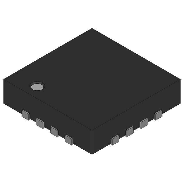
TERMINAL ASSIGNMENTS
For the ONET4291PA, a small-footprint 4-mm × 4-mm, 16-terminal QFN package is used, with a terminal pitch of
0,65 mm.
GND
DOUT+
DOUT−
GND
RGV PACKAGE
(TOP VIEW)
16
15
14
13
11
VCC
SCK 3
10
TH
SDA 4
9
5
6
7
8
DIN−
SD 2
DIN+
VCC
COC+
12
COC−
LOS 1
RTHI
P0030-01
TERMINAL DESCRIPTION
TERMINAL
TYPE
DESCRIPTION
6
Analog
Offset cancellation filter capacitor plus terminal. An external 0.1-µF filter capacitor must be
connected between this terminal and COC– (terminal 5).
COC–
5
Analog
Offset cancellation filter capacitor minus terminal. An external 0.1-µF filter capacitor must be
connected between this terminal and COC+ (terminal 6).
DIN+
7
Analog input
Non-inverted data input. On-chip 50-Ω terminated to COC+. Differentially 100-Ω terminated
to DIN–.
DIN–
8
Analog input
Inverted data input. On-chip 50-Ω terminated to COC–. Differentially 100-Ω terminated to
DIN+.
DOUT+
15
CML output
Non-inverted data output. On-chip 50-Ω back-terminated to VCC.
DOUT–
14
CML output
Inverted data output. On-chip 50-Ω back-terminated to VCC.
NAME
NO.
COC+
GND
13, 16, EP
Supply
LOS
1
Open-drain
MOS
RTHI
9
Analog
SCK
3
CMOS input
SD
2
CMOS output
SDA
4
CMOS input
Two-wire interface serial data input. Includes a 100-kΩ pullup resistor to VCC.
TH
10
Analog input
LOS threshold adjustment with resistor to GND. For use of the internal digitally controlled
resistor, connect TH with RTHI (terminal 9).
VCC
11, 12
Supply
8
Circuit ground. Exposed die pad (EP) must be grounded.
High level indicates that the input signal amplitude is below the programmed threshold level.
Open-drain output. Requires an external 10-kΩ pullup resistor to VCC for proper operation.
Digitally controlled internal resistor to ground, which can be used for LOS threshold
adjustment. A 6-bit-wide control register can be set via the two-wire interface.
Two-wire interface serial clock. Includes a 100-kΩ pullup resistor to VCC.
High level indicates that sufficient input signal amplitude is applied to the device. Low level
indicates that the input signal amplitude is below the programmed threshold level.
3.3-V, +10%/–12% supply voltage
�ONET4291PA
www.ti.com
SLLS671 – SEPTEMBER 2005
ABSOLUTE MAXIMUM RATINGS
over operating free-air temperature range (unless otherwise noted)
(1)
(2)
VCC
Supply voltage
VDIN+, VDIN–
Voltage at DIN+, DIN– (2)
0.5 V to 4 V
VLOS, VSD, VSCK, VSDA,
VCOC+, VCOC–, VRTHI,
VTH, VDOUT+, VDOUT–
Voltage at LOS, SD, SCK, SDA, COC+, COC–, RTHI, TH, DOUT+, DOUT– (2)
–0.3 V to 4 V
VDIN,DIFF
Differential voltage between DIN+ and DIN–
±1.25 V
ILOS
Current into LOS
10 mA
IDIN+, IDIN–, IDOUT+,
IDOUT–
Continuous current at inputs and outputs
20 mA
ESD
ESD rating at all terminals (HBM)
TJ,max
Maximum junction temperature
Tstg
Storage temperature range
–65°C to 85°C
TA
Characterized free-air operating temperature range
–40°C to 85°C
TLEAD
Lead temperature 1,6 mm (1/16 inch) from case for 10 seconds
(1)
(2)
–0.3 V to 4 V
4 kV
125°C
260°C
Stresses beyond those listed under "absolute maximum ratings" may cause permanent damage to the device. These are stress ratings
only, and functional operation of the device at these or any other conditions beyond those indicated under "recommended operating
conditions" is not implied. Exposure to absolute-maximum-rated conditions for extended periods may affect device reliability.
All voltage values are with respect to network ground terminal.
RECOMMENDED OPERATING CONDITIONS
over operating free-air temperature range (unless otherwise noted)
MIN
NOM
MAX
3.3
3.6
V
85
°C
VCC, VCCO
Supply voltage
2.9
TA
Operating free-air temperature
–40
CMOS input high voltage
2
UNIT
V
CMOS input low voltage
0.8
V
DC ELECTRICAL CHARACTERISTICS
over recommended operating conditions (unless otherwise noted). Typical values are at VCC = 3.3 V and TA = 25°C.
PARAMETER
VCC, VCCO
IVCC
Supply current
RIN, ROUT
(1)
MIN
TYP
MAX
2.9
3.3
3.6
VOD = 1000 mVp-p, maximum
bandwidth selected
35
50
64
VOD = 800 mVp-p, maximum
bandwidth selected
32
46
59
VOD = 600 mVp-p, maximum
bandwidth selected
28
41
53
VOD = 400 mVp-p, maximum
bandwidth selected
24
36
48
UNIT
V
mA
Ω
Data input/output resistance
Single-ended
CMOS output high voltage
ISINK = 1 mA
CMOS output low voltage
ISOURCE = 1 mA
0.5
V
LOS low voltage
ISOURCE = 1.5 mA
0.5
V
62
kΩ
Optimum LOS threshold resistor
(1)
TEST CONDITIONS
Supply voltage
50
2.3
12
V
Use of the bandwidth select switch increases current consumption. The MSB bandwidth-select bit, BW3, typically consumes 5 mA, BW2
2.6 mA, BW1 1.3 mA, and BW0 0.7 mA.
9
�ONET4291PA
www.ti.com
SLLS671 – SEPTEMBER 2005
AC ELECTRICAL CHARACTERISTICS
over recommended operating conditions (unless otherwise noted). Typical operating condition is at VCC = 3.3 V and
TA = 25°C.
PARAMETER
TEST CONDITIONS
MIN
TYP
MAX
Maximum bandwidth selected (BW3
= BW2 = BW1 = BW0 = 0)
3.5
4.5
6
Minimum bandwidth selected (BW3
= BW2 = BW1 = BW0 = 1)
0.7
f3dB-H
High-frequency –3-dB bandwidth
f3dB-L
Low-frequency –3-dB bandwidth
COC = 0.1 µF
Data rate
Maximum bandwidth selected (BW3
= BW2 = BW1 = BW0 = 0)
vIN,MIN
A
Data input sensitivity
GHz
23
4.25
1.9
2.7
VOD-min ≥ 0.95 * VOD (at VIN = 25
mVp-p) (gain limited)
8
14
mVp-p
38
43
Small-signal gain vs supply voltage
VCC
DJ
Data input overload
Deterministic jitter
17
vIN = 25 mVp-p, K28.5 at 4.25 Gbps,
maximum bandwidth
8
15
Input = 5 mVp-p, maximum
bandwidth
3
Output rise time
tF
Output fall time
Input = 10 mVp-p, maximum
bandwidth
700
850
1000
20% to 80%, vIN > 25 mVp-p,
maximum bandwidth
45
90
ps
20% to 80%, vIN > 25 mVp-p,
maximum bandwidth
45
90
ps
K28.5 pattern at 4.25 Gbps, RTH =
62 kΩ
5.5
K28.5 pattern at 4.25 Gbps, RTH =
12 kΩ
30
10
K28.5 pattern at 4.25 Gbps
mVp-p
mVp-p
1
LOS threshold variation vs supply
voltage VCC
LOS deassert time
psp-p
psRMS
1.5
LOS threshold variation vs
temperature
TLOS_DEA
mVp-p
9
tR
LOS assert time
dB
vIN = 10 mVp-p, K28.5 at 4.25 Gbps,
maximum bandwidth
800-mV output amplitude selected
(default), vIN > 25 mVp-p
LOS hysteresis
1
18
Differential-data output voltage
TLOS_AST
dB
10
VOD
LOS assert threshold range
dB
2000
Random jitter
VTH
46
2.5
vIN = 5 mVp-p, K28.5 at 4.25 Gbps,
maximum bandwidth
RJ
kHz
Gbps
Small-signal gain vs temperature
vIN,MAX
50
K28.5 at 4.25 Gbps, BER < 10–12
(noise limited)
Small-signal gain
UNIT
dB
1.5
dB
2
7.4
dB
400
1500
ns
15
80
ns
�ONET4291PA
www.ti.com
SLLS671 – SEPTEMBER 2005
TYPICAL CHARACTERISTICS
Typical operating condition is at VCC = 3.3 V and TA = 25°C.
FREQUENCY RESPONSE FOR
DIFFERENT BANDWIDTH SETTINGS
BANDWIDTH
vs
REGISTER-4 SETTING
5
45
43
4
41
Bandwidth − GHz
Gain − dB
39
37
35
33
3
2
31
1
29
27
0
25
0.1
1
00 10 20 30 40 50 60 70 80 90 A0 B0 C0 D0 E0 F0
10
Register 4 Setting − Hex
f − Frequency − GHz
G002
Figure 5.
Figure 6.
DIFFERENTIAL INPUT RETURN GAIN
vs
FREQUENCY (MAXIMUM BANDWIDTH)
RANDOM JITTER
vs
INPUT AMPLITUDE (4.25 Gbps, MAXIMUM BANDWIDTH)
0
8
−5
7
−10
6
Random Output Jitter − ps
SDD11 − Differential Input Return Gain − dB
G001
−15
−20
−25
−30
4
3
2
1
−35
−40
0.01
5
0
0.1
1
10
f − Frequency − GHz
G003
Figure 7.
0
5
10
15
20
25
30
35
40
Differential Input Voltage − mVPP
45
50
G004
Figure 8.
11
�ONET4291PA
www.ti.com
SLLS671 – SEPTEMBER 2005
TYPICAL CHARACTERISTICS (continued)
Typical operating condition is at VCC = 3.3 V and TA = 25°C.
BIT-ERROR RATIO
vs
INPUT AMPLITUDE (4.25 Gbps, MAXIMUM BANDWIDTH)
LOS ASSERT/DEASSERT VOLTAGE
vs
DIGITAL CONTROL SETTING
100
100
90
LOS Assert/Deassert Voltage − mVP-P
10-2
Bit Error Ratio
10-4
10-6
10-8
10-10
10-12
10-14
80
70
60
50
40
30
20
LOS Deassert Voltage
10
LOS Assert Voltage
10-16
0.0
0.5
1.0
1.5
2.0
2.5
0
0x40 0x38 0x30 0x28 0x20 0x18 0x10 0x08 0x00
3.0
VID − Differential Input Voltage − mVP-P
Register 5 Setting − Hex
G006
G005
Figure 9.
Figure 10.
LOS ASSERT/DEASSERT VOLTAGE
vs
THRESHOLD RESISTANCE
LOS HYSTERESIS
vs
DIGITAL CONTROL SETTING
55
6
5
45
40
LOS Hysteresis − dB
LOS Assert/Deassert Voltage − mVPP
50
35
30
25
20
LOS Deassert Voltage
15
10
5
3
2
1
LOS Assert Voltage
0
0
0x40 0x38 0x30 0x28 0x20 0x18 0x10 0x08 0x00
12 16 20 24 28 32 36 40 44 48 52 56 60
RTH − Nominal Threshold Resistor − kΩ
Figure 11.
12
4
G013
Register 5 Setting − Hex
G007
Figure 12.
�ONET4291PA
www.ti.com
SLLS671 – SEPTEMBER 2005
TYPICAL CHARACTERISTICS (continued)
Typical operating condition is at VCC = 3.3 V and TA = 25°C.
LOS HYSTERESIS
vs
THRESHOLD RESISTANCE
LOS THRESHOLD VARIATION OVER TEMPERATURE
vs
DIGITAL CONTROL SETTING
6
4.0
3.5
LOS Assert Voltage Variation − dB
LOS Hysteresis − dB
5
4
3
2
1
3.0
2.5
2.0
1.5
1.0
0.5
0
0.0
0x40 0x38 0x30 0x28 0x20 0x18 0x10 0x08 0x00
12 16 20 24 28 32 36 40 44 48 52 56 60
RTH − Nominal Threshold Resistor − kΩ
Register 5 Setting − Hex
G014
G008
OUTPUT EYE DIAGRAM AT 4.25 Gbps
AND MINIMUM INPUT VOLTAGE (5 mVp-p)
(K28.5 PATTERN, MAXIMUM BANDWIDTH)
OUTPUT EYE DIAGRAM AT 4.25 Gbps
AND MAXIMUM INPUT VOLTAGE (2000 mVp-p)
(K28.5 PATTERN, MAXIMUM BANDWIDTH)
VOD − Differential Output Voltage − 160 mV/Div
Figure 14.
VOD − Differential Output Voltage − 160 mV/Div
Figure 13.
t − Time − 50 ps/Div
t − Time − 50 ps/Div
G009
Figure 15.
G010
Figure 16.
13
�ONET4291PA
www.ti.com
SLLS671 – SEPTEMBER 2005
TYPICAL CHARACTERISTICS (continued)
Typical operating condition is at VCC = 3.3 V and TA = 25°C.
OUTPUT EYE DIAGRAM AT 1.0625 Gbps
AND MAXIMUM INPUT VOLTAGE (2000 mVp-p)
(K28.5 PATTERN, REGISTER 4 SET TO 0x70)
VOD − Differential Output Voltage − 160 mV/Div
VOD − Differential Output Voltage − 160 mV/Div
OUTPUT EYE DIAGRAM AT 1.0625 Gbps
AND MINIMUM INPUT VOLTAGE (5 mVp-p)
(K28.5 PATTERN, REGISTER 4 SET TO 0x70)
t − Time − 200 ps/Div
t − Time − 200 ps/Div
G012
G011
Figure 17.
14
Figure 18.
�ONET4291PA
www.ti.com
SLLS671 – SEPTEMBER 2005
APPLICATION INFORMATION
Figure 19 shows a typical application circuit using the ONET4291PA with a microprocessor for digital control of
the LOS threshold, output amplitude, and bandwidth.
SD
SCK
SDA
To/From Microprocessor
L1
BLM11HA102SG
VCC
R1
10 kΩ
DIN+
DIN−
DIN−
C2
0.1 µF
SD
LOS
C3
0.1 µF
DOUT+
DOUT+
DOUT−
DOUT−
GND
To/From
SFP
Connector
C4
0.1 µF
VCC
DIN+
ONET4291PA
16-Pin QFN
VCC
From
Transimpedance
Amplifier (ROSA)
COC−
GND
TH
C1
0.1 µF
COC+
RTHI
C5
0.1 µF
SCK
SDA
LOS
C6
0.1 µF
GND
S0099-01
Figure 19. Basic Application Circuit With Digital Control
15
�ONET4291PA
www.ti.com
SLLS671 – SEPTEMBER 2005
APPLICATION INFORMATION (continued)
Figure 20 shows a typical application without digital control. In this case, the output amplitude and bandwidth are
fixed. The LOS threshold is adjusted by means of a resistor connected to the TH terminal.
L1
BLM11HA102SG
VCC
R1
10 kΩ
DIN+
DIN−
DIN−
C2
0.1 µF
SD
LOS
C3
0.1 µF
DOUT+
DOUT+
DOUT−
DOUT−
GND
To/From
SFP
Connector
C4
0.1 µF
VCC
DIN+
ONET4291PA
16-Pin QFN
VCC
From
Transimpedance
Amplifier (ROSA)
COC−
GND
TH
C1
0.1 µF
COC+
RTHI
C5
0.1 µF
SCK
SDA
LOS
RTH
12 kΩ − 62 kΩ
C6
0.1 µF
GND
S0099-02
Figure 20. Basic Application Circuit With External LOS Threshold Resistor
16
�PACKAGE OPTION ADDENDUM
www.ti.com
10-Dec-2020
PACKAGING INFORMATION
Orderable Device
Status
(1)
Package Type Package Pins Package
Drawing
Qty
Eco Plan
(2)
Lead finish/
Ball material
MSL Peak Temp
Op Temp (°C)
Device Marking
(3)
(4/5)
(6)
ONET4291PARGVR
ACTIVE
VQFN
RGV
16
2500
RoHS & Green
NIPDAU
Level-2-260C-1 YEAR
-40 to 85
4291PA
ONET4291PARGVT
ACTIVE
VQFN
RGV
16
250
RoHS & Green
NIPDAU
Level-2-260C-1 YEAR
-40 to 85
4291PA
(1)
The marketing status values are defined as follows:
ACTIVE: Product device recommended for new designs.
LIFEBUY: TI has announced that the device will be discontinued, and a lifetime-buy period is in effect.
NRND: Not recommended for new designs. Device is in production to support existing customers, but TI does not recommend using this part in a new design.
PREVIEW: Device has been announced but is not in production. Samples may or may not be available.
OBSOLETE: TI has discontinued the production of the device.
(2)
RoHS: TI defines "RoHS" to mean semiconductor products that are compliant with the current EU RoHS requirements for all 10 RoHS substances, including the requirement that RoHS substance
do not exceed 0.1% by weight in homogeneous materials. Where designed to be soldered at high temperatures, "RoHS" products are suitable for use in specified lead-free processes. TI may
reference these types of products as "Pb-Free".
RoHS Exempt: TI defines "RoHS Exempt" to mean products that contain lead but are compliant with EU RoHS pursuant to a specific EU RoHS exemption.
Green: TI defines "Green" to mean the content of Chlorine (Cl) and Bromine (Br) based flame retardants meet JS709B low halogen requirements of