���������
��
��
��� �������
��������
SLLS601A − MAY 2004 − REVISED OCTOBER 2005
D Surface Mount Small Footprint 4 mm ×
features
D
D
D
D
D
D
D
D
D
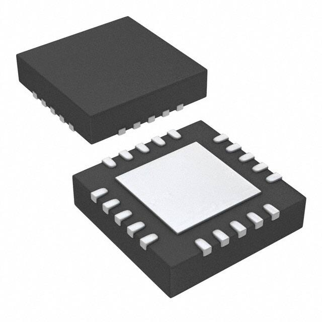
4 mm, 20-Pin QFN Package
10.7-Gbps Operation
116-mW Power Consumption
Input Offset Cancellation
High Input Dynamic Range
Output Disable
CML Data Outputs
2-mVp-p Input Sensitivity
Loss of Signal Detection
Single 3.3-V Supply
applications
D SONET/SDH Transmission Systems at
OC−192
D 10-Gbps Fibre Channel Receivers
D 10-Gbps Ethernet Receivers
description
The ONET9901PA is a versatile high-speed limiting amplifier for multiple fiber optic applications with data rates
up to 10.7 Gbps.
This device provides a typical gain of about 42 dB, which ensures a fully differential output swing for input signals
as low as 2 mVp-p.
The high input signal dynamic range ensures low jitter output signals, even when overdriven with input signal
swings as high as 1200 mVp-p.
The ONET9901PA comprises an adjustable loss of signals detection. The threshold voltage can be defined by
means of an external resistor.
The ONET9901PA is available in a small footprint 4 mm × 4 mm, 20-pin QFN package.
The ONET9901PA is a power efficient limiting amplifier with power dissipation as low as 116 mW typical from
a single 3.3-V supply. The part is characterized for operation from 0°C to 85°C.
Please be aware that an important notice concerning availability, standard warranty, and use in critical applications of
Texas Instruments semiconductor products and disclaimers thereto appears at the end of this data sheet.
Copyright 2005, Texas Instruments Incorporated
���������� � � �������!��� �� "#��$�! �� �� �#�%�"�!��� &�!$
���&#"!� "������ !� ��$"���"�!���� �$� !'$ !$��� �� �$(�� ���!�#�$�!�
�!��&��& )�����!*
���&#"!��� ���"$����+ &�$� ��! �$"$�����%* ��"%#&$
!$�!��+ �� �%% �����$!$��
POST OFFICE BOX 655303
• DALLAS, TEXAS 75265
1
����������
��
��
��� �������
��������
SLLS601A − MAY 2004 − REVISED OCTOBER 2005
block diagram
A simplified block diagram of the ONET9901PA is shown in Figure 1.
These compact, low power 10.7-Gbps limiting amplifier consists of a high-speed data path with offset
cancellation block, a loss of signal detection block, and a bandgap voltage reference and bias current generation
block.
The limiting amplifier requires a single 3.3-V supply voltage. All circuit parts are described in detail below.
COC2 COC1
VCC
Offset
Cancellation
GND
VCCI
VCCO
GND
DIN+
+
DIN−
−
GND
Input Buffer
+
+
+
Gain Stage
Gain Stage
DOUT+
+
DOUT−
−
Gain Stage
CML
Output
Buffer
DISABLE
Bandgap Voltage
Reference and
Bias Current
Generation
Loss of Signal
Detection
TH
LOS
LOSEN
Figure 1. Block Diagram
high-speed data path
The high-speed data signal is applied to the data path by means of the input signal pins DIN+/DIN–. The data
path consists of the input stage with 2 × 50-Ω on-chip line termination to VCCI, three gain stages, which provide
the required typical gain of about 42 dB, and a CML output stage.
Next to the input signal pins shielding ground pins GND are provided. These pins must have a good external
ground connection for best performance at low input signal amplitudes.
The amplified data output signal is available at the output pins DOUT+/DOUT–, which provide 2 × 50-Ω
back-termination to VCCO. The output stage also includes a disable function, controlled by the signal applied
to the DISABLE input pin.
An offset cancellation compensates inevitable internal offset voltages and thus ensures proper operation even
for small input data signals.
The low frequency cutoff is as low as 42 kHz with the built-in filter capacitor.
For applications, which require even lower cutoff frequencies, an additional external filter capacitor may be
connected to the COC1/COC2 pins.
loss of signal and RSSI detection
The output signal of the input buffer is monitored by the loss of signal detection circuitry. This circuit block
compares the input signal to a threshold, which can be programmed by means of an external resistor connected
to the TH pin. If the input signal falls below the specified threshold, a loss of signal is indicated at the LOS pin.
For use in applications, which do not require a loss of signal function, this circuit block can be shut down by
connecting the LOSEN pin to GND.
2
POST OFFICE BOX 655303
• DALLAS, TEXAS 75265
����������
��
��
��� �������
��������
SLLS601A − MAY 2004 − REVISED OCTOBER 2005
bandgap voltage and bias generation
The ONET9901PA limiting amplifier is supplied by a single 3.3-V ±10% supply voltage connected to the VCC,
VCCI, and VCCO pins. This voltage is referred to ground (GND).
An on-chip bandgap voltage circuitry generates a supply voltage independent reference from which all other
internally required voltages and bias currents are derived.
package
DISABLE
COC1
VCC
COC2
VCC1
For the ONET9901PA a small footprint 4 mm × 4 mm, 20-pin QFN package is used with a lead pitch of 0,5 mm.
The pinout is shown in Figure 2.
20 19 18 17 16
1
13 DOUT−
12 VCCO
N.C. 5
11 GND
8
9 10
TH
7
LOS
6
GND
DIN− 3
GND 4
GND
15 VCCO
14 DOUT+
LOSEN
DIN+ 2
GND
Figure 2. Pinout of ONET9901PA in a 4 mm y 4 mm 20-Pin QFN Package
POST OFFICE BOX 655303
• DALLAS, TEXAS 75265
3
����������
��
��
��� �������
��������
SLLS601A − MAY 2004 − REVISED OCTOBER 2005
terminal functions
The following table shows a pin description for the ONET9901PA in a 4 mm x 4 mm 20-pin QFN package.
TERMINAL
TYPE
NAME
NO.
GND
1, 4, 6, 8,
11, EP
Ground
DESCRIPTION
Circuit ground. The exposed die pad (EP) must be grounded.
DIN+
2
Analog in
Noninverted data input. On-chip 50-Ω terminated to VCCI
DIN–
3
Analog in
Inverted data input. On-chip 50-Ω terminated to VCCI
NC
5
LOSEN
7
CMOS in
Not connected
LOS
9
CMOS out
A high level indicates that the input signal amplitude is below the programmed threshold level.
LOS threshold adjustment with resistor to GND
TH
10
Analog in
VCCO
12, 15
Supply
Enables loss off signal circuitry when set to high level (VCC)
3.3-V ±10% supply voltage for output stage
DOUT–
13
CML out
Inverted data output. On-chip 50-Ω back-terminated to VCCO
DOUT+
14
CML out
Noninverted data output. On-chip 50-Ω back-terminated to VCCO
DISABLE
16
CMOS in
Disables CML output stage when set to high level
VCC
17
Supply
3.3-V ±10% supply voltage
COC1
18
Analog
Offset cancellation filter capacitor terminal 1. Connect an additional filter capacitor between this pin
and COC2 (pin 19). To disable the offset cancellation loop, connect COC1 and COC2 (pins 18 and
19).
COC2
19
Analog
Offset cancellation filter capacitor terminal 2. Connect an additional filter capacitor between this pin
and COC1 (pin 18). To disable the offset cancellation loop, connect COC1 and COC2 (pins 18 and
19).
VCCI
20
Supply
3.3-V ±10% supply voltage for input stage.
absolute maximum ratings
over operating free-air temperature range unless otherwise noted†
VCC, VCCI, VCCO
VDIN+, VDIN−
Supply voltage, See Note 1
VTH, VDISABLE, VLOS, VLOSEN,
VDOUT+, VDOUT–,VCOC1, VCOC2
Voltage at TH, DISABLE, LOS, LOSEN, DOUT+, DOUT–, COC1, COC2,
See Note 1
VCOC,DIFF
VDIN,DIFF
Differential voltage between COC1 and COC2
ILOS
IDIN+, IDIN−, IDOUT+, IDOUT–
Current into LOS
ESD
ESD rating at all pins except DIN+, DIN–, DOUT+, DOUT–
ESD
ESD rating at DIN+, DIN–, DOUT+, DOUT–
TJ(max)
Tstg
Maximum junction temperature
TA
TL
Characterized free-air operating temperature range
Voltage at DIN+, DIN–, See Note 1
Differential voltage between DIN+ and DIN–
Continuous current at inputs and outputs
Storage temperature range
Lead temperature 1,6 mm (1/16 inch) from case for 10 seconds
VALUE
UNIT
–0.3 to 4
V
0.5 to 4
V
–0.3 to 4
V
±1
V
±2.5
V
–1 to 9
mA
–25 to 25
mA
2
kV (HBM)
1
kV (HBM)
125
°C
−65 to 85
°C
0 to 85
°C
260
°C
† Stresses beyond those listed under “absolute maximum ratings” may cause permanent damage to the device. These are stress ratings only, and
functional operation of the device at these or any other conditions beyond those indicated under “recommended operating conditions” is not
implied. Exposure to absolute-maximum-rated conditions for extended periods may affect device reliability.
NOTE 1: All voltage values are with respect to network ground terminal.
4
POST OFFICE BOX 655303
• DALLAS, TEXAS 75265
����������
��
��
��� �������
��������
SLLS601A − MAY 2004 − REVISED OCTOBER 2005
recommended operating conditions
MIN
TYP
MAX
UNIT
Supply voltage, VCC, VCCI, VCCO
3
3.3
3.6
V
Operating free-air temperature, TA
0
85
°C
dc electrical characteristics
over recommended operating conditions (unless otherwise noted)
PARAMETER
TEST CONDITIONS
MIN
TYP
MAX
3
3.3
3.6
LOSEN = high, DISABLE = low,
VTH = 50 mVp−p
35
55
LOSEN = low, DISABLE = low
25
35
VCC, VCCI,VCCO Supply voltage
ICC
Supply current
DISABLE = high
VOD
Differential data output voltage swing
VOC
ro
Common-mode output voltage
Data output resistance
Single ended
r(IND)
Data input resistance
Differential
V(INMIN)
Data input sensitivity
VOD(min) ≥ 0.95 x VOD (at VIN = 10 mV)
BER < 10–12, 223–1 PRBS, 10.7 Gbps
V(INMAX)
Data input overload
DISABLE = low
190
0.25
10
240
400
DISABLE. LOSEN
CMOS input low voltage
DISABLE, LOSEN
mVp−p
Ω
100
Ω
V
mVp−p
6
mVp−p
V
2.1
0.6
2.4
0.4
5 mVp−p < VTH < 40 mVp−p
V
V
LOS low voltage
LOS hysteresis
mA
2
LOS high voltage
VTH
V
VCC – 0.075
50
1200
CMOS input high voltage
UNIT
2.5
4.5
LOS assert threshold range
6.2
2−50
V
dB
mVp−p
ac electrical characteristics
over recommended operating conditions (unless otherwise noted) typical operating condition is at VCC = 3.3 V and
TA = 25°C
PARAMETER
BW
TEST CONDITIONS
MIN
Small-signal bandwidth
Low frequency −3-dB bandwidth
TYP
MAX
10
COC = open
42
GHz
75
8
Data rate
UNIT
10.7
kHz
Gb/s
5 mVp−p, 10-mVp−p input, K28.5 pattern at 10.7 Gbps
5.2
16
800 mVp−p, 1200-mVp−p input, K28.5 pattern at 10.7 Gbps
1.8
11
1.1
DJ
Deterministic jitter
RJ
Random jitter
20 mVp−p up to 1200-mVp−p input
0.6
tr
tf
Output rise time
20% to 80%
20
psRMS
ps
Output fall time
20% to 80%
20
ps
tDIS
tLOS
Disable response time
20
ns
250
ns
LOS assert/deassert time
POST OFFICE BOX 655303
• DALLAS, TEXAS 75265
psp−p
5
����������
��
��
��� �������
��������
SLLS601A − MAY 2004 − REVISED OCTOBER 2005
APPLICATION INFORMATION
Figure 3 shows the ONET9901PA in a 4 mm × 4 mm 20-pin package connected with an ac-coupled interface
to the data signal source as well as to the output load.
Besides the ac-coupling capacitors C1 through C4 in the input and output data signal lines, the only required
external component is the LOS threshold setting resistor RTH. In addition, an optional external filter capacitor
(COC) may be used if a lower cutoff frequency is desired.
DISABLE
DIN−
C2
GND
DISABLE
VCC
COC1
VCCI
DIN+
C1
COC2
COC
Optional
DOUT+
DIN+
ONET9901PA
20 Pin QFN
DIN−
DOUT−
C3
C4
DOUT+
DOUT−
VCCO
TH
LOS
GND
GND
GND
NC
LOSEN
GND
VCC
VCCO
LOS
LOSEN
RTH
Figure 3. Basic Application Circuit for the ONET9901PA in a 4 mm × 4 mm, 20-Pin QFN Package With
AC-Coupled I/Os
6
POST OFFICE BOX 655303
• DALLAS, TEXAS 75265
�PACKAGE OPTION ADDENDUM
www.ti.com
6-Nov-2008
PACKAGING INFORMATION
Orderable Device
Status (1)
Package
Type
Package
Drawing
Pins Package Eco Plan (2)
Qty
ONET9901PARGP
NRND
QFN
RGP
20
91
Green (RoHS &
no Sb/Br)
CU NIPDAU
Level-2-260C-1 YEAR
ONET9901PARGPG4
NRND
QFN
RGP
20
91
Green (RoHS &
no Sb/Br)
CU NIPDAU
Level-2-260C-1 YEAR
Lead/Ball Finish
MSL Peak Temp (3)
(1)
The marketing status values are defined as follows:
ACTIVE: Product device recommended for new designs.
LIFEBUY: TI has announced that the device will be discontinued, and a lifetime-buy period is in effect.
NRND: Not recommended for new designs. Device is in production to support existing customers, but TI does not recommend using this part in
a new design.
PREVIEW: Device has been announced but is not in production. Samples may or may not be available.
OBSOLETE: TI has discontinued the production of the device.
(2)
Eco Plan - The planned eco-friendly classification: Pb-Free (RoHS), Pb-Free (RoHS Exempt), or Green (RoHS & no Sb/Br) - please check
http://www.ti.com/productcontent for the latest availability information and additional product content details.
TBD: The Pb-Free/Green conversion plan has not been defined.
Pb-Free (RoHS): TI's terms "Lead-Free" or "Pb-Free" mean semiconductor products that are compatible with the current RoHS requirements
for all 6 substances, including the requirement that lead not exceed 0.1% by weight in homogeneous materials. Where designed to be soldered
at high temperatures, TI Pb-Free products are suitable for use in specified lead-free processes.
Pb-Free (RoHS Exempt): This component has a RoHS exemption for either 1) lead-based flip-chip solder bumps used between the die and
package, or 2) lead-based die adhesive used between the die and leadframe. The component is otherwise considered Pb-Free (RoHS
compatible) as defined above.
Green (RoHS & no Sb/Br): TI defines "Green" to mean Pb-Free (RoHS compatible), and free of Bromine (Br) and Antimony (Sb) based flame
retardants (Br or Sb do not exceed 0.1% by weight in homogeneous material)
(3)
MSL, Peak Temp. -- The Moisture Sensitivity Level rating according to the JEDEC industry standard classifications, and peak solder
temperature.
Important Information and Disclaimer:The information provided on this page represents TI's knowledge and belief as of the date that it is
provided. TI bases its knowledge and belief on information provided by third parties, and makes no representation or warranty as to the
accuracy of such information. Efforts are underway to better integrate information from third parties. TI has taken and continues to take
reasonable steps to provide representative and accurate information but may not have conducted destructive testing or chemical analysis on
incoming materials and chemicals. TI and TI suppliers consider certain information to be proprietary, and thus CAS numbers and other limited
information may not be available for release.
In no event shall TI's liability arising out of such information exceed the total purchase price of the TI part(s) at issue in this document sold by TI
to Customer on an annual basis.
Addendum-Page 1
����IMPORTANT NOTICE
Texas Instruments Incorporated and its subsidiaries (TI) reserve the right to make corrections, modifications, enhancements, improvements,
and other changes to its products and services at any time and to discontinue any product or service without notice. Customers should
obtain the latest relevant information before placing orders and should verify that such information is current and complete. All products are
sold subject to TI’s terms and conditions of sale supplied at the time of order acknowledgment.
TI warrants performance of its hardware products to the specifications applicable at the time of sale in accordance with TI’s standard
warranty. Testing and other quality control techniques are used to the extent TI deems necessary to support this warranty. Except where
mandated by government requirements, testing of all parameters of each product is not necessarily performed.
TI assumes no liability for applications assistance or customer product design. Customers are responsible for their products and
applications using TI components. To minimize the risks associated with customer products and applications, customers should provide
adequate design and operating safeguards.
TI does not warrant or represent that any license, either express or implied, is granted under any TI patent right, copyright, mask work right,
or other TI intellectual property right relating to any combination, machine, or process in which TI products or services are used. Information
published by TI regarding third-party products or services does not constitute a license from TI to use such products or services or a
warranty or endorsement thereof. Use of such information may require a license from a third party under the patents or other intellectual
property of the third party, or a license from TI under the patents or other intellectual property of TI.
Reproduction of TI information in TI data books or data sheets is permissible only if reproduction is without alteration and is accompanied
by all associated warranties, conditions, limitations, and notices. Reproduction of this information with alteration is an unfair and deceptive
business practice. TI is not responsible or liable for such altered documentation. Information of third parties may be subject to additional
restrictions.
Resale of TI products or services with statements different from or beyond the parameters stated by TI for that product or service voids all
express and any implied warranties for the associated TI product or service and is an unfair and deceptive business practice. TI is not
responsible or liable for any such statements.
TI products are not authorized for use in safety-critical applications (such as life support) where a failure of the TI product would reasonably
be expected to cause severe personal injury or death, unless officers of the parties have executed an agreement specifically governing
such use. Buyers represent that they have all necessary expertise in the safety and regulatory ramifications of their applications, and
acknowledge and agree that they are solely responsible for all legal, regulatory and safety-related requirements concerning their products
and any use of TI products in such safety-critical applications, notwithstanding any applications-related information or support that may be
provided by TI. Further, Buyers must fully indemnify TI and its representatives against any damages arising out of the use of TI products in
such safety-critical applications.
TI products are neither designed nor intended for use in military/aerospace applications or environments unless the TI products are
specifically designated by TI as military-grade or "enhanced plastic." Only products designated by TI as military-grade meet military
specifications. Buyers acknowledge and agree that any such use of TI products which TI has not designated as military-grade is solely at
the Buyer's risk, and that they are solely responsible for compliance with all legal and regulatory requirements in connection with such use.
TI products are neither designed nor intended for use in automotive applications or environments unless the specific TI products are
designated by TI as compliant with ISO/TS 16949 requirements. Buyers acknowledge and agree that, if they use any non-designated
products in automotive applications, TI will not be responsible for any failure to meet such requirements.
Following are URLs where you can obtain information on other Texas Instruments products and application solutions:
Products
Applications
Audio
www.ti.com/audio
Communications and Telecom www.ti.com/communications
Amplifiers
amplifier.ti.com
Computers and Peripherals
www.ti.com/computers
Data Converters
dataconverter.ti.com
Consumer Electronics
www.ti.com/consumer-apps
DLP® Products
www.dlp.com
Energy and Lighting
www.ti.com/energy
DSP
dsp.ti.com
Industrial
www.ti.com/industrial
Clocks and Timers
www.ti.com/clocks
Medical
www.ti.com/medical
Interface
interface.ti.com
Security
www.ti.com/security
Logic
logic.ti.com
Space, Avionics and Defense
www.ti.com/space-avionics-defense
Power Mgmt
power.ti.com
Transportation and
Automotive
www.ti.com/automotive
Microcontrollers
microcontroller.ti.com
Video and Imaging
www.ti.com/video
RFID
www.ti-rfid.com
Wireless
www.ti.com/wireless-apps
RF/IF and ZigBee® Solutions
www.ti.com/lprf
TI E2E Community Home Page
e2e.ti.com
Mailing Address: Texas Instruments, Post Office Box 655303, Dallas, Texas 75265
Copyright © 2011, Texas Instruments Incorporated
�


 工商网监
湘ICP备2023018690号
工商网监
湘ICP备2023018690号