SO−8
Single/Dual
SSOP−16
Quad
(Obsolete)
SOT−23−5
Single
MSOP Dual
OPA237
OPA2237
OPA4237
SBOS057A − OCTOBER 1996 − REVISED FEBRUARY 2007
SINGLE-SUPPLY OPERATIONAL AMPLIFIERS
MicroAmplifierE Series
FEATURES
DESCRIPTION
D MICRO-SIZE, MINIATURE PACKAGES:
The OPA237 op amp family is one of Texas Instruments’
MicroAmplifier series of miniature products. In addition
to small size, these devices feature low offset voltage, low
quiescent current, low bias current, and a wide supply
range. Single, dual, and quad versions have identical
specifications for maximum design flexibility. They are
ideal
for
single-supply,
battery-operated,
and
space-limited applications, such as PCMCIA cards and
other portable instruments.
− Single: SOT23-5, SO-8
− Dual: MSOP-8, SO-8
− Quad: SSOP-16 (Obsolete)
LOW OFFSET VOLTAGE: 750µV max
D
D WIDE SUPPLY RANGE:
D
D
− Single Supply: +2.7V to +36V
− Dual Supply: +1.35V to +18V
LOW QUIESCENT CURRENT: 350µV max
WIDE BANDWIDTH: 1.5MHz
OPA237 series op amps can operate from either single or
dual supplies. When operated from a single supply, the
input common-mode range extends below ground and the
output can swing to within 10mV of ground. Dual and quad
designs feature completely independent circuitry for
lowest crosstalk and freedom from interaction.
APPLICATIONS
D
D
D
D
D
BATTERY-POWERED INSTRUMENTS
PORTABLE DEVICES
PCMCIA CARDS
MEDICAL INSTRUMENTS
TEST EQUIPMENT
Single, dual, and quad are offered in space-saving
surface-mount packages. The single version is available
in the ultra-miniature 5-lead SOT23-5 and SO-8
surface-mount. The dual version comes in a miniature
MSOP-8 and SO-8 surface-mount. The quad version is
obsolete. MSOP-8 has the same lead count as a SO-8 but
half the size. The SOT23-5 is even smaller at one-fourth
the size of an SO-8. All are specified for −40°C to +85°C
operation. A macromodel is available for design analysis.
OPA237
Out
1
V−
2
+In
3
5
V+
4
−In
SOT23−5
OPA4237
OPA237
OPA2237
Out A
1
−In A
2
A
NC
1
8
NC
Out A
1
−In
2
7
V+
−In A
2
+In
3
6
Output
+In A
3
V−
4
5
NC
V−
A
B
4
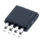
SO−8
Out D
15
−In D
D
+In A
3
14
+In D
Out B
V+
4
13
V−
−In B
+In B
5
12
+In C
+In B
−In B
6
11
−In C
Out B
7
10
Out C
NC
8
9
8
V+
7
6
5
16
B
C
SO−8, MSOP−8
NC
SSOP−16
Please be aware that an important notice concerning availability, standard warranty, and use in critical applications of Texas Instruments
semiconductor products and disclaimers thereto appears at the end of this data sheet.
MicroAmplifier is a trademark of Texas Instruments. All other trademarks are the property of their respective owners.
Copyright 1996-2007, Texas Instruments Incorporated
��������� �
�
��
�������� �� ������� �� �
����������� ����� ��������
���
��� �� �����
�������� ��� ��� ����� �
����� ����������� �������� ���������
���������� ���������! ���� ��� ����������� ������� ������! �
��� �����������
www.ti.com
���
"#$
��
""#$
��
%"#$
www.ti.com
SBOS057A − OCTOBER 1996 − REVISED FEBRUARY 2007
ABSOLUTE MAXIMUM RATINGS(1)
Supply Voltage, V+ to V− . . . . . . . . . . . . . . . . . . . . . . . . . . . . . . . . . . . . . . 36V
Input Voltage . . . . . . . . . . . . . . . . . . . . . . . . . . . . . . (V−) −0.7V to (V+) +0.7V
Output Short-Circuit(2) . . . . . . . . . . . . . . . . . . . . . . . . . . . . . . . . . . Continuous
Operating Temperature Range . . . . . . . . . . . . . . . . . . . . . . −55°C to +125°C
Storage Temperature Range . . . . . . . . . . . . . . . . . . . . . . . . −55°C to +125°C
Junction Temperature Range . . . . . . . . . . . . . . . . . . . . . . . . . . . . . . . +150°C
(1) Stresses above these ratings may cause permanent damage.
Exposure to absolute maximum conditions for extended periods
may degrade device reliability. These are stress ratings only, and
functional operation of the device at these or any other conditions
beyond those specified is not implied.
This integrated circuit can be damaged by ESD. Texas
Instruments recommends that all integrated circuits be
handled with appropriate precautions. Failure to observe
proper handling and installation procedures can cause damage.
ESD damage can range from subtle performance degradation to
complete device failure. Precision integrated circuits may be more
susceptible to damage because very small parametric changes could
cause the device not to meet its published specifications.
(2) Short circuit to ground, one amplifier per package.
PACKAGE/ORDERING INFORMATION(1)
PRODUCT
PACKAGE−LEAD
PACKAGE DRAWING
PACKAGE MARKING
SOT23-5
DBV
A37A
SO-8
D
OPA237UA
MSOP-8
DGK
B37A
SO-8
D
OPA2237UA
SSOP-16
DBQ
OPA4237UA
Single
OPA237NA
OPA237UA
Dual
OPA2237EA
OPA2237UA
Quad(2)
OPA4237UA
(1) For the most current package and ordering information, see the Package Option Addendum at the end of this document, or see the TI website
at www.ti.com.
(2) Quad version is obsolete.
2
���
"#$
��
""#$
��
%"#$
www.ti.com
SBOS057A − OCTOBER 1996 − REVISED FEBRUARY 2007
ELECTRICAL CHARACTERISTICS: VS = +5V
Boldface limits apply over the specified temperature range, TA = −40°C to +85°C.
At TA = +25°C, VS = +5V, RL = 10kΩ, connected to VS/2, unless otherwise noted.
OPA237UA, NA
OPA2237UA, EA
OPA4237UA
PARAMETER
CONDITIONS
MIN
TYP
MAX
UNITS
VCM = 2.5V
±250
±750
µV
Specified Temperature Range
+2
+5
µV/°C
10
30
µV/V
OFFSET VOLTAGE
Input Offset Voltage
vs Temperature(1)
vs Power Supply (PSRR)
VS = +2.7V to +36V
Channel Separation (dual and quad)
µV/V
0.5
INPUT BIAS CURRENT
Input Bias Current(2)
VCM = 2.5V
−10
−40
nA
Input Offset Current
VCM = 2.5V
±0.5
±10
nA
NOISE
Input Voltage Noise, f = 0.1 to 10Hz
1
µVPP
Input Voltage Noise Density, f = 1kHz
28
nV/√Hz
Current Noise Density, f = 1kHz
60
fA/√Hz
INPUT VOLTAGE RANGE
Common-Mode Voltage Range
−0.2
Common-Mode Rejection Ratio
VCM = −0.2V to 3.5V
78
(V+) −1.5
V
86
dB
5 • 106 || 4
5 • 109 || 2
Ω || pF
88
dB
INPUT IMPEDANCE
Differential
Common-Mode
Ω || pF
OPEN-LOOP GAIN
Open-Loop Voltage Gain
VO = 0.5V to 4V
80
FREQUENCY RESPONSE
Gain-Bandwidth Product
1.4
MHz
G=1
0.5
V/µs
G = −1, 3V Step, CL = 100pF
11
µs
G = −1, 3V Step, CL = 100pF
16
µs
Slew Rate
Settling Time, 0.1%
0.01%
OUTPUT
Voltage Output, Positive
RL = 100kΩ to Ground
(V+) −1
(V+) −0.75
V
Negative
RL = 100kΩ to Ground
0.01
0.001
V
Positive
RL = 100kΩ to 2.5V
(V+) −1
(V+) −0.75
V
Negative
RL = 100kΩ to 2.5V
0.12
0.04
V
Positive
RL = 10kΩ to 2.5V
(V+) −1
(V+) −0.75
V
Negative
RL = 10kΩ to 2.5V
0.5
0.35
V
−10/+4
mA
Short-Circuit Current
Capacitive Load Drive (stable operation)
See Typical Characteristic Curves
POWER SUPPLY
Specified Operating Voltage
Operating Range
+5
+2.7
Quiescent Current (per amplifier)
170
V
+36
V
350
µA
TEMPERATURE RANGE
Specified Range
−40
+85
°C
Operating Range
−55
+125
°C
Storage Range
−55
+125
°C
Thermal Resistance, qJA
SOT23-5
200
°C/W
MSOP-8
150
°C/W
SSOP-16 (Obsolete)
150
°C/W
SO-8
150
°C/W
(1) Specified by wafer-level test to 95% confidence.
(2) Positive conventional current flows into the input terminals.
3
���
"#$
��
""#$
��
%"#$
www.ti.com
SBOS057A − OCTOBER 1996 − REVISED FEBRUARY 2007
ELECTRICAL CHARACTERISTICS: VS = +2.7V
Boldface limits apply over the specified temperature range, TA = −40°C to +85°C.
At TA = +25°C, VS = +2.7V , RL = 10kΩ, connected to VS/2, unless otherwise noted.
OPA237UA, NA
OPA2237UA, EA
OPA4237UA
PARAMETER
CONDITIONS
MIN
TYP
MAX
UNITS
VCM = 1V
±250
±750
µV
Specified Temperature Range
+2
+5
µV/°C
10
30
µV/V
OFFSET VOLTAGE
Input Offset Voltage
vs Temperature(1)
vs Power Supply (PSRR)
VS = +2.7V to +36V
Channel Separation (dual and quad)
µV/V
0.5
INPUT BIAS CURRENT
Input Bias Current(2)
VCM = 1V
−10
−40
nA
Input Offset Current
VCM = 1V
±0.5
±10
nA
NOISE
Input Voltage Noise, f = 0.1 to 10Hz
1
µVPP
Input Voltage Noise Density, f = 1kHz
28
nV/√Hz
Current Noise Density, f = 1kHz
60
fA/√Hz
INPUT VOLTAGE RANGE
Common-Mode Voltage Range
−0.2
Common-Mode Rejection Ratio
VCM = −0.2V to 1.2V
75
(V+) −1.5
V
85
dB
5 • 106 || 4
5 • 109 || 2
Ω || pF
88
dB
INPUT IMPEDANCE
Differential
Common-Mode
Ω || pF
OPEN-LOOP GAIN
Open-Loop Voltage Gain
VO = 0.5V to 1.7V
80
FREQUENCY RESPONSE
Gain-Bandwidth Product
1.2
MHz
G=1
0.5
V/µs
G = −1, 1V Step, CL = 100pF
5
µs
G = −1, 1V Step, CL = 100pF
8
µs
Slew Rate
Settling Time, 0.1%
0.01%
OUTPUT
Voltage Output, Positive
RL = 100kΩ to Ground
(V+) −1
(V+) −0.75
V
Negative
RL = 100kΩ to Ground
0.01
0.001
V
Positive
RL = 100kΩ to 1.35V
(V+) −1
(V+) −0.75
V
Negative
RL = 100kΩ to 1.35V
0.06
0.02
V
Positive
RL = 10kΩ to 1.35V
(V+) −1
(V+) −0.75
V
Negative
RL = 10kΩ to 1.35V
0.3
0.2
V
−5/+3.5
mA
Short-Circuit Current
Capacitive Load Drive (stable operation)
See Typical Characteristic Curves
POWER SUPPLY
Specified Operating Voltage
Operating Range
+2.7
+2.7
Quiescent Current (per amplifier)
160
V
+36
V
350
µA
TEMPERATURE RANGE
Specified Range
−40
+85
°C
Operating Range
−55
+125
°C
Storage Range
−55
+125
°C
Thermal Resistance, qJA
SOT23-5
200
°C/W
MSOP-8
150
°C/W
SSOP-16 (Obsolete)
150
°C/W
SO-8
150
°C/W
(1) Specified by wafer-level test to 95% confidence.
(2) Positive conventional current flows into the input terminals.
4
���
"#$
��
""#$
��
%"#$
www.ti.com
SBOS057A − OCTOBER 1996 − REVISED FEBRUARY 2007
ELECTRICAL CHARACTERISTICS: VS = +15V
Boldface limits apply over the specified temperature range, TA = −40°C to +85°C.
At TA = +25°C, VS = ±15V , RL = 10kΩ, connected to VS/2, unless otherwise noted.
OPA237UA, NA
OPA2237UA, EA
OPA4237UA
PARAMETER
CONDITIONS
MIN
TYP
MAX
UNITS
VCM = 0V
±350
±950
µV
Specified Temperature Range
+2.5
+7
µV/°C
10
30
µV/V
OFFSET VOLTAGE
Input Offset Voltage
vs Temperature(1)
VS = ±1.35V to ±18V
vs Power Supply (PSRR)
Channel Separation (dual and quad)
µV/V
0.5
INPUT BIAS CURRENT
Input Bias Current(2)
VCM = 0V
−8.5
−40
nA
Input Offset Current
VCM = 0V
±0.5
±10
nA
NOISE
Input Voltage Noise, f = 0.1 to 10Hz
1
µVPP
Input Voltage Noise Density, f = 1kHz
28
nV/√Hz
Current Noise Density, f = 1kHz
60
fA/√Hz
INPUT VOLTAGE RANGE
Common-Mode Voltage Range
(V−)−0.2
Common-Mode Rejection Ratio
VCM = −15V to 13.5V
80
(V+) −1.5
V
90
dB
5 • 106 || 4
5 • 109 || 2
Ω || pF
88
dB
INPUT IMPEDANCE
Differential
Common-Mode
Ω || pF
OPEN-LOOP GAIN
Open-Loop Voltage Gain
VO = −14V to 13.8V
80
FREQUENCY RESPONSE
Gain-Bandwidth Product
1.5
MHz
G=1
0.5
V/µs
G = −1, 10V Step, CL = 100pF
18
µs
G = −1, 10V Step, CL = 100pF
21
µs
Slew Rate
Settling Time, 0.1%
0.01%
OUTPUT
Voltage Output, Positive
RL = 100kΩ
(V+) −1.2
(V+) −0.9
V
Negative
RL = 100kΩ
(V−) +0.5
(V−) +0.3
V
Positive
RL = 10kΩ
(V+) −1.2
(V+) −0.9
V
Negative
RL = 10kΩ
(V−) +1
(V−) +0.85
V
−8/+4.5
mA
Short-Circuit Current
Capacitive Load Drive (stable operation)
See Typical Characteristic Curves
POWER SUPPLY
±15
Specified Operating Range
Operating Range
±1.35
±200
Quiescent Current (per amplifier)
V
±18
V
±475
µA
TEMPERATURE RANGE
Specified Range
−40
+85
°C
Operating Range
−55
+125
°C
Storage Range
−55
+125
°C
Thermal Resistance, qJA
SOT23-5
200
°C/W
MSOP-8
150
°C/W
SSOP-16 (Obsolete)
150
°C/W
SO-8
150
°C/W
(1) Specified by wafer-level test to 95% confidence.
(2) Positive conventional current flows into the input terminals.
5
���
"#$
��
""#$
��
%"#$
www.ti.com
SBOS057A − OCTOBER 1996 − REVISED FEBRUARY 2007
TYPICAL CHARACTERISTICS
At TA = +25°C and RL = 10kΩ, unless otherwise noted.
POWER SUPPLY and COMMON−MODE REJECTION
vs FREQUENCY
OPEN−LOOP GAIN/PHASE vs FREQUENCY
100
120
CL = 100pF
G
+PSR (VS = +5V, ±15V)
0
−45
Φ
VS = ±15V
40
−90
20
−135
0
PSR, CMR (dB)
60
100
Phase (_)
Voltage Gain (dB)
80
−180
VS = +2.7V, +5V
10
100
1k
10k
100k
1M
60
40
+PSR
(VS = +2.7V)
−PSR
(VS = ±15V)
20
−20
1
CMR (VS = +2.7V, +5V or ±15V)
80
0
10M
10
100
1k
Frequency (Hz)
10k
100k
1M
10M
Frequency (Hz)
INPUT NOISE AND CURRENT NOISE
SPECTRAL DENSITY vs FREQUENCY
CHANNEL SEPARATION vs FREQUENCY
130
Channel Separation (dB)
Voltage Noise (nV/√Hz)
Current Noise (fA/√Hz)
1k
Current Noise
100
Voltage Noise
120
110
100
90
80
10
10
1
100
1k
10k
Dual and quad devices.
G = 1, all channels.
Quad measured channel
A to D or B to C other
combinations yield improved
rejection.
10
100k
100
1k
Frequency (Hz)
14
−12
−11
12
VS = +2.7V, +5V
Input Bias Current (nA)
Input Bias Current (nA)
100k
INPUT BIAS CURRENT
vs INPUT COMMON−MODE VOLTAGE
INPUT BIAS CURRENT vs TEMPERATURE
10
8
VS = ±15V
6
VS = +2.7V
VS = +5V
−10
−9
VS = ±15V
−8
−7
4
−75
−50
−25
0
25
50
Temperature (_ C)
6
10k
Frequency (Hz)
75
100
125
−6
−15
−10
−5
0
5
Common−Mode Voltage (V)
10
15
���
"#$
��
""#$
��
%"#$
www.ti.com
SBOS057A − OCTOBER 1996 − REVISED FEBRUARY 2007
TYPICAL CHARACTERISTICS (Continued)
At TA = +25°C and RL = 10kΩ, unless otherwise noted.
OFFSET VOLTAGE
PRODUCTION DISTRIBUTION
OFFSET VOLTAGE
PRODUCTION DISTRIBUTION
9
VS = +2.7V, +5V
7.5
5
2.5
0.2%
8
0.4%
0.7%
6
5
4
3
2
1
0.1%
0.1%
0
−950
−850
−750
−650
−550
−450
−350
−250
−150
−50
50
150
250
350
450
550
650
750
850
950
750
650
550
450
350
250
50
150
−50
−150
−250
−350
−450
−550
−650
−750
0
Offset Voltage (µV)
Offset Voltage (µV)
OFFSET VOLTAGE DRIFT
PRODUCTION DISTRIBUTION
OFFSET VOLTAGE DRIFT
PRODUCTION DISTRIBUTION
30
16
25
20
15
10
5
0.2%
0.2%
12
10
8
6
4
0.6% 0.2% 0.4%
2
0
0.2%
VS = ±15V
AOL, CMR, PSR (dB)
6
4
2
8
7
7.5
6
6.5
5
5.5
4
4.5
3
CMR
AOL
PSR
110
8
0.2%
0.4%
AOL, CMR, PSR vs TEMPERATURE
120
Typical production
distribution of packaged
units. Single, dual,
and quad units included.
10
3.5
2
Offset Voltage Drift (µV/_C)
OFFSET VOLTAGE DRIFT
PRODUCTION DISTRIBUTION
12
2.5
1
0.5
11.5
10.5
9.5
8.5
7.5
6.5
5.5
4.5
3.5
2.5
1.5
0.5
0
Offset Voltage Drift (µV/_C)
100
VS = +2.7V, +5V, ±15V
VS = ±15V
VS = +2.7V, +5V
90
80
VS = ±15V
VS = +2.7V, +5V
70
0.4%
60
Offset Voltage Drift (µV/_ C)
8
7.5
7
6.5
6
5.5
5
4.5
4
3.5
3
2
2.5
1.5
1
0
0.5
Percent of Amplifiers (%)
Typical production
distribution of packaged
units. Single, dual,
and quad units included.
VS = +5V
14
Percent of Amplifiers (%)
Typical production
distribution of packaged
units. Single, dual,
and quad units included.
VS = +2.7V
Percent of Amplifiers (%)
7
VS = ±15V
Typical production
distribution of packaged
units. Single, dual,
and quad units included.
1.5
10
Typical production
distribution of packaged
units. Single, dual,
and quad units included.
Percent of Amplifiers (%)
Percent of Amplifiers (%)
12.5
−75
−50
−25
0
25
50
75
100
125
Temperature (_C)
7
���
"#$
��
""#$
��
%"#$
www.ti.com
SBOS057A − OCTOBER 1996 − REVISED FEBRUARY 2007
TYPICAL CHARACTERISTICS (Continued)
At TA = +25°C and RL = 10kΩ, unless otherwise noted.
20mV/div
SMALL−SIGNAL STEP RESPONSE
(G = 1, CL = 220pF, VS = +5V)
20mV/div
SMALL−SIGNAL STEP RESPONSE
(G = 1, CL = 100pF, VS = +5V)
1µs/div
2µs/div
SETTLING TIME vs GAIN
LARGE−SIGNAL STEP RESPONSE
(G = 1, CL = 100pF, VS = +5V)
100
VS = ±15V,
10V Step
1V/div
Settling Time (µs)
VS = +5V,
3V Step
10
VS = +2.7V,
1V Step
0.01%
0.1%
1
−1
−10
10µs/div
SMALL−SIGNAL OVERSHOOT
vs LOAD CAPACITANCE
OUTPUT VOLTAGE SWING vs OUTPUT CURRENT
V+
70
Sourcing Current
(V+) −1
+25_ C
(V+) −1.5
50
+125_C
−55_ C
(V−) +2
+125_ C
Sinking Current
−55_ C
(V−) +1.5
+5V, ±15V
40
30
20
(V−) +1
+25_C
(V−) +0.5
10
+125_C
V−
0
1
2
3
Output Current (mA)
8
G = +1, V S = +2.7V, +5V
G = +1, V S = ±15V
G = −1, V S = ±15V
G = −2, V S = +2.7V, +5V
G = −10, V S = +2.7V,
60
Overshoot (%)
Output Voltage Swing (V)
(V+) −0.5
(V+) −2
−100
Gain (V/V)
4
5
0
10
100
1k
Load Capacitance (pF)
10k
���
"#$
��
""#$
��
%"#$
www.ti.com
SBOS057A − OCTOBER 1996 − REVISED FEBRUARY 2007
TYPICAL CHARACTERISTICS (Continued)
At TA = +25°C and RL = 10kΩ, unless otherwise noted.
MAXIMUM OUTPUT VOLTAGE
vs FREQUENCY
QUIESCENT CURRENT vs TEMPERATURE
300
VS = ±15V
Maximum output voltage
without slew−rate induced
distortion
20
15
10
VS = +5V
5
200
150
VS = +5V
VS = +2.7V
100
50
0
1k
VS = ±15V
250
VS = +2.7V
10k
100k
−75
1M
−50
−25
0
25
50
75
100
125
Temperature (_ C)
Frequency (Hz)
SHORT−CIRCUIT CURRENT vs TEMPERATURE
12
VS = +5V
Short−Circuit Current (mA)
Output Voltage (VPP)
25
Quiescent Current (µA)
30
10
8
VS = ±15V
VS = +2.7V
6
−
ISC
4
+
ISC
2
VS = ±15V
VS = +2.7V
VS = +5V
0
−75
−50
−25
0
25
50
75
100
125
Temperature (_C)
9
���
"#$
��
""#$
��
%"#$
www.ti.com
SBOS057A − OCTOBER 1996 − REVISED FEBRUARY 2007
APPLICATION INFORMATION
OPA237 series op amps remain stable with capacitive
loads up to 4,000pF, if sinking current and up to 10,000pF,
if sourcing current. Furthermore, in single-supply
applications where the load is connected to ground, the op
amp is only sourcing current, and as shown Figure 1, can
drive 10,000pF with output currents up to 1.5mA.
OPA237 series op amps are unity-gain stable and suitable
for a wide range of general-purpose applications. Power
supply pins should be bypassed with 10nF ceramic
capacitors.
OPERATING VOLTAGE
100k
OPA237 series op amps operate from single (+2.7V to
+36V) or dual (±1.35V to ±18V) supplies with excellent
performance. Most behavior remains unchanged
throughout the full operating voltage range. Parameters
which vary significantly with operating voltage are shown
in typical performance curves. Specifications are
production tested with +2.7V, +5V, and ±15V supplies.
Capacitive Load (pF)
OPERATION NOT
RECOMMENDED
10k
1k
VS = +5V, ±15V
100
OUTPUT CURRENT AND STABILITY
VS = +2.7V
OPA237 series op amps can drive large capacitive loads.
However, under certain limited output conditions any op
amp may become unstable. Figure 1 shows the region
where the OPA237 has a potential for instability. These
load conditions are rarely encountered, especially for
single supply applications. For example, take the case
when a +5V supply with a 10kΩ load to VS/2 is used.
10
−2
−1.5
−1
−0.5
0
0.5
1
To Load
R5
383kΩ
IH
High−Side
Current Sense
R3
38.3kΩ
V+
−In
A1
Out
+In OPA237
R4
20kΩ
V+ for A1, A2
+
VO = 10 • IH • RH
R2 V−
19.1kΩ
R2 and R4 divide down the
common−mode input to A1.
R8
100kΩ
2.7V to = ±15V
V− for A1, A2
V+
−In
A2
Out
VO = 10 • IL • RL
+In OPA237
V−
R7
9.09kΩ
R6
10kΩ
RL
10Ω
Low−Side
Current Sense
Common−mode range of A2
extends to V− for low−side sensing
Optional for IB Cancellation
(R7 = R6 II R8)
To Load
IL
NOTE: Low and high−side sensing circuits can be used independently.
Figure 2. Low and High-Side Battery Current Sensing
10
2
Figure 1. Stability-Capacitive Load vs Output
Current
RH
10Ω
R1
38.3kΩ
1.5
Output Current (mA)
�PACKAGE OPTION ADDENDUM
www.ti.com
13-Jul-2022
PACKAGING INFORMATION
Orderable Device
Status
(1)
Package Type Package Pins Package
Drawing
Qty
Eco Plan
(2)
Lead finish/
Ball material
MSL Peak Temp
Op Temp (°C)
Device Marking
(3)
Samples
(4/5)
(6)
OPA2237EA/250
ACTIVE
VSSOP
DGK
8
250
RoHS & Green
NIPDAUAG
Level-2-260C-1 YEAR
B37A
Samples
OPA2237EA/2K5
ACTIVE
VSSOP
DGK
8
2500
RoHS & Green
NIPDAUAG
Level-2-260C-1 YEAR
B37A
Samples
OPA2237UA
ACTIVE
SOIC
D
8
75
RoHS & Green
NIPDAU
Level-3-260C-168 HR
OPA
2237UA
Samples
OPA2237UA/2K5
ACTIVE
SOIC
D
8
2500
RoHS & Green
NIPDAU
Level-3-260C-168 HR
OPA
2237UA
Samples
OPA2237UAE4
ACTIVE
SOIC
D
8
75
RoHS & Green
NIPDAU
Level-3-260C-168 HR
OPA
2237UA
Samples
OPA237NA/250
ACTIVE
SOT-23
DBV
5
250
RoHS & Green
NIPDAU
Level-2-260C-1 YEAR
-40 to 70
A37A
Samples
OPA237NA/250E4
ACTIVE
SOT-23
DBV
5
250
RoHS & Green
NIPDAU
Level-2-260C-1 YEAR
-40 to 70
A37A
Samples
OPA237NA/3K
ACTIVE
SOT-23
DBV
5
3000
RoHS & Green
NIPDAU
Level-2-260C-1 YEAR
-40 to 70
A37A
Samples
OPA237NA/3KE4
ACTIVE
SOT-23
DBV
5
3000
RoHS & Green
NIPDAU
Level-2-260C-1 YEAR
-40 to 70
A37A
Samples
OPA237UA
ACTIVE
SOIC
D
8
75
RoHS & Green
NIPDAU
Level-3-260C-168 HR
-40 to 70
OPA
237UA
Samples
OPA237UA/2K5
ACTIVE
SOIC
D
8
2500
RoHS & Green
NIPDAU
Level-3-260C-168 HR
-40 to 70
OPA
237UA
Samples
OPA237UA/2K5G4
ACTIVE
SOIC
D
8
2500
TBD
Call TI
Call TI
-40 to 70
-40 to 85
(1)
The marketing status values are defined as follows:
ACTIVE: Product device recommended for new designs.
LIFEBUY: TI has announced that the device will be discontinued, and a lifetime-buy period is in effect.
NRND: Not recommended for new designs. Device is in production to support existing customers, but TI does not recommend using this part in a new design.
PREVIEW: Device has been announced but is not in production. Samples may or may not be available.
OBSOLETE: TI has discontinued the production of the device.
(2)
RoHS: TI defines "RoHS" to mean semiconductor products that are compliant with the current EU RoHS requirements for all 10 RoHS substances, including the requirement that RoHS substance
do not exceed 0.1% by weight in homogeneous materials. Where designed to be soldered at high temperatures, "RoHS" products are suitable for use in specified lead-free processes. TI may
reference these types of products as "Pb-Free".
RoHS Exempt: TI defines "RoHS Exempt" to mean products that contain lead but are compliant with EU RoHS pursuant to a specific EU RoHS exemption.
Green: TI defines "Green" to mean the content of Chlorine (Cl) and Bromine (Br) based flame retardants meet JS709B low halogen requirements of


 工商网监
湘ICP备2023018690号
工商网监
湘ICP备2023018690号
