Sample &
Buy
Product
Folder
Support &
Community
Tools &
Software
Technical
Documents
OPA227, OPA2227, OPA4227
OPA228, OPA2228, OPA4228
SBOS110B – MAY 1998 – REVISED JUNE 2015
OPAx22x High Precision, Low Noise Operational Amplifiers
1 Features
3 Description
•
•
The OPAx22x series operational amplifiers combine
low noise and wide bandwidth with high precision to
make them the ideal choice for applications requiring
both AC and precision DC performance.
1
•
•
•
•
•
•
•
•
•
Low Noise: 3nV/√Hz
Wide Bandwidth:
– OPA227: 8 MHz, 2.3 V/μs
– OPA228: 33 MHz, 10 V/μs
Settling Time: 5 μs
(Significant Improvement Over OP-27)
High CMRR: 138 dB
High Open-loop Gain: 160 dB
Low Input Bias Current: 10 nA Maximum
Low Offset Voltage: 75 µV Maximum
Wide Supply Range: ±2.5 V to ±18 V
OPA227 Replaces OP-27, LT1007, MAX427
OPA228 Replaces OP-37, LT1037, MAX437
Single, Dual, and Quad Versions
The OPAx227 is unity-gain stable and features high
slew rate (2.3V/µs) and wide bandwidth (8MHz). The
OPAx228 is optimized for closed-loop gains of 5 or
greater, and offers higher speed with a slew rate of
10V/µs and a bandwidth of 33MHz.
The OPAx227 and OPAx228 series operational
amplifiers are ideal for professional audio equipment.
In addition, low quiescent current and low cost make
them ideal for portable applications requiring high
precision.
The OPAx227 and OPAx228 series operational
amplifiers are pin-for-pin replacements for the
industry standard OP-27 and OP-37 with substantial
improvements across the board. The dual and quad
versions are available for space savings and per
channel cost reduction.
2 Applications
•
•
•
•
•
•
•
•
Data Acquisition
Telecom Equipment
Geophysical Analysis
Vibration Analysis
Spectral Analysis
Professional Audio Equipment
Active Filters
Power Supply Controls
The OPAx227, OPAx228, are available in DIP-8 and
SO-8 packages. The OPA4227 and OPA4228 are
available in DIP-14 and SO-14 packages with
standard pin configurations. Operation is specified
from –40°C to 85°C.
Device Information(1)
PART NUMBER
Input Referred Noise
INPUT VOLTAGE AND CURRENT NOISE
SPECTRAL DENSITY vs FREQUENCY
Voltage Noise (nV/√Hz)
Current Noise (fA/√Hz)
100k
10k
BODY SIZE (NOM)
OPA227
OPA228
9.81 mm × 6.35 mm
SOIC (8)
4.90 mm × 3.91 mm
OPA2227
OPA2228
PDIP (8)
9.81 mm × 6.35 mm
SOIC (8)
4.90 mm × 3.91 mm
OPA4227
OPA4228
PDIP (14)
19.30 mm × 6.35 mm
SOIC (14)
8.65 mm × 3.91 mm
(1) For all available packages, see the orderable addendum at
the end of the data sheet.
Current Noise
1k
PACKAGE
PDIP (8)
100
10
Voltage Noise
1
0.1
1
10
100
1k
10k
Frequency (Hz)
1
An IMPORTANT NOTICE at the end of this data sheet addresses availability, warranty, changes, use in safety-critical applications,
intellectual property matters and other important disclaimers. PRODUCTION DATA.
�OPA227, OPA2227, OPA4227
OPA228, OPA2228, OPA4228
SBOS110B – MAY 1998 – REVISED JUNE 2015
www.ti.com
Table of Contents
1
2
3
4
5
6
Features ..................................................................
Applications ...........................................................
Description .............................................................
Revision History.....................................................
Pin Configuration and Functions .........................
Specifications.........................................................
6.1
6.2
6.3
6.4
6.5
6.6
6.7
6.8
7
1
1
1
2
3
5
Absolute Maximum Ratings ...................................... 5
ESD Ratings.............................................................. 5
Recommended Operating Conditions....................... 5
Thermal Information: OPA227U/UA and
OPA228U/UA ............................................................ 5
Thermal Information: OPA227P/PA and
OPA228P/PA ............................................................. 6
Electrical Characteristics: OPAx227 Series (VS = ±5
V to ±15 V) ................................................................. 7
Electrical Characteristics: OPAx228 Series (VS = ±5
V to ±15 V) ................................................................. 8
Typical Characteristics ............................................ 10
Detailed Description ............................................ 16
7.1 Overview ................................................................. 16
7.2 Functional Block Diagram ....................................... 16
7.3 Feature Description................................................. 16
7.4 Device Functional Modes........................................ 23
8
Application and Implementation ........................ 24
8.1 Application Information............................................ 24
8.2 Typical Application .................................................. 26
9 Power Supply Recommendations...................... 29
10 Layout................................................................... 29
10.1 Layout Guidelines ................................................. 29
10.2 Layout Example .................................................... 30
11 Device and Documentation Support ................. 31
11.1
11.2
11.3
11.4
11.5
11.6
Device Support ....................................................
Documentation Support ........................................
Related Links ........................................................
Trademarks ...........................................................
Electrostatic Discharge Caution ............................
Glossary ................................................................
31
31
31
31
32
32
12 Mechanical, Packaging, and Orderable
Information ........................................................... 32
4 Revision History
NOTE: Page numbers for previous revisions may differ from page numbers in the current version.
Changes from Revision A (January 2005) to Revision B
•
2
Page
Added ESD Ratings table, Feature Description section, Device Functional Modes, Application and Implementation
section, Power Supply Recommendations section, Layout section, Device and Documentation Support section, and
Mechanical, Packaging, and Orderable Information section .................................................................................................. 1
Submit Documentation Feedback
Copyright © 1998–2015, Texas Instruments Incorporated
Product Folder Links: OPA227 OPA2227 OPA4227 OPA228 OPA2228 OPA4228
�OPA227, OPA2227, OPA4227
OPA228, OPA2228, OPA4228
www.ti.com
SBOS110B – MAY 1998 – REVISED JUNE 2015
5 Pin Configuration and Functions
OPA227, OPA228: P or D Package
8-Pin PDIP or 8-Pin SOIC
Top View
Trim
1
8
Trim
–In
2
7
V+
+In
3
6
Output
V–
4
5
NC
OPA2227, OPA2228: P or D Package
8-Pin PDIP or 8-Pin SOIC
Top View
Out A
–In A
1
A
2
+In A
3
V–
4
B
8
V+
7
Out B
6
–In B
5
+In B
DIP-8, SO-8
DIP-8, SO-8
NC = Not Connected
OPA4227, OPA4228: N or D Package
14-Pin PDIP or 14-Pin-SOIC
Top View
Out A
1
14
Out D
–In A
2
13
–In D
A
D
+In A
3
12
+In D
V+
4
11
V–
+In B
5
10
+In C
B
C
–In B
6
9
–In C
Out B
7
8
Out C
DIP-14, SO-14
Pin Functions: OPA227 and OPA228
PIN
NAME
I/O
PDIP, SOIC
DESCRIPTION
Offset Trim
1
I
Input offset voltage trim (leave floating if not used)
-In
2
I
Inverting input
+In
3
I
Noninverting input
V-
4
—
Negative (lowest) power supply
NC
5
—
No internal connection (can be left floating)
Output
6
O
Output
V+
7
—
Positive (highest) power supply
Offset Trim
8
—
Input offset voltage trim (leave floating if not used)
Pin Functions: OPA2227 and OPA2228
PIN
I/O
DESCRIPTION
NAME
PDIP, SOIC
Out A
1
O
Output channel A
–In A
2
I
Inverting input channel A
+In A
3
I
Noninverting input channel A
V-
4
—
+In B
5
I
Noninverting input channel B
–In B
6
I
Inverting input channel B
Out B
7
O
Output channel B
V+
8
—
Positive (highest) power supply
Copyright © 1998–2015, Texas Instruments Incorporated
Negative (lowest) power supply
Submit Documentation Feedback
Product Folder Links: OPA227 OPA2227 OPA4227 OPA228 OPA2228 OPA4228
3
�OPA227, OPA2227, OPA4227
OPA228, OPA2228, OPA4228
SBOS110B – MAY 1998 – REVISED JUNE 2015
www.ti.com
Pin Functions: OPA4227 and OPA4228
PIN
I/O
DESCRIPTION
NAME
PDIP, SOIC
Out A
1
O
Output channel A
-In A
2
I
Inverting input channel A
+In A
3
I
Noninverting input channel A
V+
4
—
+In B
5
I
Noninverting input channel B
-In B
6
I
Inverting input channel B
Out B
7
O
Output channel B
Out C
8
O
Output channel C
-In C
9
I
Inverting input channel C
+In C
10
I
Noninverting input channel C
V-
11
—
+In D
12
I
Noninverting input channel D
-In D
13
I
Inverting input channel D
Out D
14
O
Output channel D
4
Submit Documentation Feedback
Positive (highest) power supply
Negative (lowest) power supply
Copyright © 1998–2015, Texas Instruments Incorporated
Product Folder Links: OPA227 OPA2227 OPA4227 OPA228 OPA2228 OPA4228
�OPA227, OPA2227, OPA4227
OPA228, OPA2228, OPA4228
www.ti.com
SBOS110B – MAY 1998 – REVISED JUNE 2015
6 Specifications
6.1 Absolute Maximum Ratings
over operating free-air temperature range (unless otherwise noted)
(1)
MIN
MAX
UNIT
36
V
Supply voltage, Vs = (V+) - (V-)
Signal input terminals
Voltage
(V–) – 0.7
(V+) +0.7
V
20
mA
125
°C
150
°C
150
°C
Current
Output short-circuit (2)
Continuous
Operating temperature
–55
Junction temperature
Tstg
(1)
(2)
Storage temperature
–65
Stresses beyond those listed under Absolute Maximum Ratings may cause permanent damage to the device. These are stress ratings
only, which do not imply functional operation of the device at these or any other conditions beyond those indicated under Recommended
Operating Conditions. Exposure to absolute-maximum-rated conditions for extended periods may affect device reliability.
Short-circuit to ground, one amplifier per package
6.2 ESD Ratings
V(ESD)
(1)
Electrostatic discharge
Human-body model (HBM), per ANSI/ESDA/JEDEC JS-001
(1)
VALUE
UNIT
±2000
V
JEDEC document JEP155 states that 500-V HBM allows safe manufacturing with a standard ESD control process.
6.3 Recommended Operating Conditions
over operating free-air temperature range (unless otherwise noted)
MIN
NOM
MAX
UNIT
Supply voltage, Vs = (V+) - (V-)
±2.5
±15
±18
V
Specified temperature
–40
85
°C
6.4 Thermal Information: OPA227U/UA and OPA228U/UA
THERMAL METRIC
(1)
OPA227U/UA
OPA228U/UA
OPA2227U/UA
OPA2228U/UA
OPA4227UA
OPA4228UA
D (SOIC)
D (SOIC)
D (SOIC)
14 PINS
UNIT
8 PINS
8 PINS
RθJA
Junction-to-ambient thermal resistance
110.1
101.9
65
°C/W
RθJC(top)
Junction-to-case (top) thermal resistance
52.2
46.3
23.1
°C/W
RθJB
Junction-to-board thermal resistance
52.3
45.5
20.3
°C/W
ψJT
Junction-to-top characterization parameter
10.4
6.6
1.8
°C/W
ψJB
Junction-to-board characterization parameter
51.5
42.8
19.9
°C/W
RθJC(bot)
Junction-to-case (bottom) thermal resistance
N/A
N/A
N/A
°C/W
(1)
For more information about traditional and new thermal metrics, see the Semiconductor and IC Package Thermal Metrics application
report, SPRA953.
Copyright © 1998–2015, Texas Instruments Incorporated
Submit Documentation Feedback
Product Folder Links: OPA227 OPA2227 OPA4227 OPA228 OPA2228 OPA4228
5
�OPA227, OPA2227, OPA4227
OPA228, OPA2228, OPA4228
SBOS110B – MAY 1998 – REVISED JUNE 2015
www.ti.com
6.5 Thermal Information: OPA227P/PA and OPA228P/PA
THERMAL METRIC
OPA227P/PA
OPA228P/PA
(1)
P (PDIP)
D (SOIC)
N (PDIP)
8 PINS
8 PINS
14 PINS
UNIT
RθJA
Junction-to-ambient thermal resistance
48.9
110.1
65.5
°C/W
RθJC(top)
Junction-to-case (top) thermal resistance
37.7
52.2
20
°C/W
RθJB
Junction-to-board thermal resistance
26.1
52.3
25.9
°C/W
ψJT
Junction-to-top characterization parameter
15.1
10.4
1.9
°C/W
ψJB
Junction-to-board characterization parameter
26
51.5
25.3
°C/W
RθJC(bot)
Junction-to-case (bottom) thermal resistance
N/A
N/A
N/A
°C/W
(1)
6
For more information about traditional and new thermal metrics, see the Semiconductor and IC Package Thermal Metrics application
report, SPRA953.
Submit Documentation Feedback
Copyright © 1998–2015, Texas Instruments Incorporated
Product Folder Links: OPA227 OPA2227 OPA4227 OPA228 OPA2228 OPA4228
�OPA227, OPA2227, OPA4227
OPA228, OPA2228, OPA4228
www.ti.com
SBOS110B – MAY 1998 – REVISED JUNE 2015
6.6 Electrical Characteristics: OPAx227 Series (VS = ±5 V to ±15 V)
At TA = 25°C, and RL = 10 kΩ, unless otherwise noted.
PARAMETER
OPA227PA, UA
OPA2227PA, UA
OPA4227PA, UA
OPA227P, U
OPA2227P, U
TEST CONDITIONS
MIN
TYP
MAX
MIN
UNIT
TYP
MAX
±10
±200
OFFSET VOLTAGE
VOS
Input Offset Voltage
±5
TA = –40°C to 85°C
±75
±100
±200
µV
µV
dVOS/dT
vs Temperature
TA = –40°C to 85°C
±0.1
±0.6
±0.3
±2
µV/°C
PSRR
vs Power Supply
VS = ±2.5 V to ±18 V
±0.5
±2
±0.5
±2
µV/V
TA = –40°C to 85°C
±2
vs Time
±2
0.2
Channel Separation (dual, quad)
µV/V
0.2
µV/mo
DC
0.2
0.2
µV/V
f = 1 kHz, RL = 5 kΩ
110
110
dB
INPUT BIAS CURRENT
IB
Input Bias Current
±2.5
±10
TA = –40°C to 85°C
IOS
±2.5
±10
Input Offset Current
±2.5
±10
TA = –40°C to 85°C
±2.5
±10
±10
nA
±10
nA
±10
nA
±10
nA
NOISE
Input Voltage Noise, f = 0.1 Hz to 10 Hz
en
in
Input Voltage Noise
Density
f = 10 Hz
Current Noise Density
90
90
nVp-p
15
15
nVrms
3.5
3.5
nV/√Hz
f = 100 Hz
3
3
nV/√Hz
f = 1 kHz
3
3
nV/√Hz
f = 1 kHz
0.4
0.4
pA/√Hz
INPUT VOLTAGE RANGE
VCM
Common-Mode Voltage Range
CMRR
Common-Mode Rejection
(V–)+2
VCM = (V–)+2 V to (V+)–2 V
120
TA = –40°C to 85°C
120
(V+)–2
138
(V–)+2
(V+)–2
120
138
V
dB
120
dB
INPUT IMPEDANCE
Differential
Common-Mode
VCM = (V–)+2 V to (V+)–2 V
107 || 12
107 || 12
Ω || pF
9
9
Ω || pF
10 || 3
10 || 3
OPEN-LOOP GAIN
AOL
Open-Loop Voltage Gain
VO = (V–)+2 V to (V+)–2 V,
RL = 10 kΩ
132
TA = –40°C to 85°C
132
VO = (V–)+3.5V to (V+)–3.5 V,
RL = 600 Ω
132
TA = –40°C to 85°C
132
160
132
160
dB
132
160
dB
132
160
dB
132
dB
FREQUENCY RESPONSE
GBW
Gain Bandwidth Product
SR
Slew Rate
8
MHz
2.3
V/µs
0.1%
G = 1, 10 V Step, CL = 100 pF
5
5
µs
0.01%
G = 1, 10 V Step, CL = 100 pF
5.6
5.6
µs
Overload Recovery Time
VIN × G = VS
1.3
1.3
µs
Total Harmonic Distortion + Noise
f = 1 kHz, G = 1, VO = 3.5 Vrms
0.00005%
0.00005%
Voltage Output
RL = 10 kΩ
(V–)+2
(V+)–2
(V–)+2
(V+)–2
V
RL = 10 kΩ
(V–)+2
(V+)–2
(V–)+2
(V+)–2
V
RL = 600 Ω
(V–)+3.5
(V+)–3.5
(V–)+3.5
(V+)–3.5
V
RL = 600 Ω
(V–)+3.5
(V+)–3.5
(V–)+3.5
(V+)–3.5
V
Settling Time
THD+N
8
2.3
OUTPUT
TA = –40°C to 85°C
TA = –40°C to 85°C
ISC
Short-Circuit Current
CLOAD
Capacitive Load Drive
±45
ZO
Open-loop output impedance
f = 1 MHz
Copyright © 1998–2015, Texas Instruments Incorporated
±45
See Typical Characteristics
See Typical Characteristics
27
27
Submit Documentation Feedback
Product Folder Links: OPA227 OPA2227 OPA4227 OPA228 OPA2228 OPA4228
mA
Ω
7
�OPA227, OPA2227, OPA4227
OPA228, OPA2228, OPA4228
SBOS110B – MAY 1998 – REVISED JUNE 2015
www.ti.com
Electrical Characteristics: OPAx227 Series (VS = ±5 V to ±15 V) (continued)
At TA = 25°C, and RL = 10 kΩ, unless otherwise noted.
PARAMETER
OPA227PA, UA
OPA2227PA, UA
OPA4227PA, UA
OPA227P, U
OPA2227P, U
TEST CONDITIONS
MIN
TYP
MAX
MIN
TYP
UNIT
MAX
POWER SUPPLY
VS
IQ
Specified Voltage Range
±5
±15
±5
±15
Operating Voltage Range
±2.5
±18
±2.5
±18
V
±3.8
mA
±4.2
mA
Quiescent Current (per amplifier)
IO = 0
±3.7
±3.8
IO = 0
±3.7
±4.2
V
TA = –40°C to 85°C
TEMPERATURE RANGE
θJA
Specified Range
–40
85
–40
85
°C
Operating Range
–55
125
–55
125
°C
Storage Range
–65
150
–65
150
°C
Thermal Resistance
SO-8 Surface Mount
150
150
°C/W
DIP-8
100
100
°C/W
DIP-14
80
80
°C/W
100
100
°C/W
SO-14 Surface Mount
6.7 Electrical Characteristics: OPAx228 Series (VS = ±5 V to ±15 V)
At TA = 25°C, and RL = 10 kΩ, unless otherwise noted.
PARAMETER
OPA228PA, UA
OPA2228PA, UA
OPA4228PA, UA
OPA228P, U
OPA2228P, U
TEST CONDITIONS
MIN
TYP
MAX
MIN
UNIT
TYP
MAX
±10
±200
OFFSET VOLTAGE
VOS
Input Offset Voltage
±5
TA = –40°C to 85°C
±75
±100
±200
µV
µV
dVOS/dT
vs Temperature
TA = –40°C to 85°C
±0.1
±0.6
±0.3
±2
µV/°C
PSRR
vs Power Supply
VS = ±2.5 V to ±18 V
±0.5
±2
±0.5
±2
µV/V
TA = –40°C to 85°C
±2
vs Time
±2
0.2
Channel Separation (dual, quad)
µV/V
0.2
µV/mo
DC
0.2
0.2
µV/V
f = 1kHz, RL = 5 kΩ
110
110
dB
INPUT BIAS CURRENT
IB
Input Bias Current
±2.5
TA = –40°C to 85°C
IOS
±10
±2.5
±10
Input Offset Current
±2.5
TA = –40°C to 85°C
±10
±2.5
±10
±10
nA
±10
nA
±10
nA
±10
nA
NOISE
Input Voltage Noise, f = 0.1 Hz to 10 Hz
en
in
Input Voltage Noise
Density
f = 10 Hz
Current Noise Density
90
90
nVp-p
15
15
nVrms
3.5
3.5
nV/√Hz
f = 100 Hz
3
3
nV/√Hz
f = 1 kHz
3
3
nV/√Hz
f = 1 kHz
0.4
0.4
pA/√Hz
INPUT VOLTAGE RANGE
VCM
Common-Mode Voltage Range
CMRR
Common-Mode Rejection
(V–)+2
VCM = (V–)+2 V to (V+)–2 V
120
TA = –40°C to 85°C
120
(V+)–2
138
(V–)+2
(V+)–2
120
138
120
V
dB
dB
INPUT IMPEDANCE
Differential
Common-Mode
8
VCM = (V–)+2 V to (V+)–2 V
Submit Documentation Feedback
107 || 12
107 || 12
Ω || pF
9
9
Ω || pF
10 || 3
10 || 3
Copyright © 1998–2015, Texas Instruments Incorporated
Product Folder Links: OPA227 OPA2227 OPA4227 OPA228 OPA2228 OPA4228
�OPA227, OPA2227, OPA4227
OPA228, OPA2228, OPA4228
www.ti.com
SBOS110B – MAY 1998 – REVISED JUNE 2015
Electrical Characteristics: OPAx228 Series (VS = ±5 V to ±15 V) (continued)
At TA = 25°C, and RL = 10 kΩ, unless otherwise noted.
PARAMETER
OPA228PA, UA
OPA2228PA, UA
OPA4228PA, UA
OPA228P, U
OPA2228P, U
TEST CONDITIONS
MIN
TYP
VO = (V–)+2 V to (V+)–2 V,
RL = 10 kΩ
132
160
TA = –40°C to 85°C
132
VO = (V–)+3.5 V to (V+)–3.5 V,
RL = 600 Ω
132
TA = –40°C to 85°C
132
MAX
MIN
TYP
132
160
UNIT
MAX
OPEN-LOOP GAIN
AOL
Open-Loop Voltage Gain
dB
132
160
dB
132
160
dB
132
dB
FREQUENCY RESPONSE
Minimum Closed-Loop Gain
GBW
Gain Bandwidth Product
SR
Slew Rate
5
5
V/V
33
33
MHz
11
11
V/µs
0.1%
G = 5, 10 V Step, CL = 100 pF, CF =
12 pF
1.5
1.5
µs
0.01%
G = 5, 10 V Step, CL = 100 pF, CF =
12 pF
2
2
µs
0.6
0.6
µs
0.00005%
0.00005%
Settling Time
THD+N
Overload Recovery Time
VIN × G = VS
Total Harmonic Distortion + Noise
f = 1 kHz, G = 5, VO = 3.5 Vrms
Voltage Output
RL = 10 kΩ
(V–)+2
(V+)–2
(V–)+2
(V+)–2
V
RL = 10 kΩ
(V–)+2
(V+)–2
(V–)+2
(V+)–2
V
RL = 600 Ω
(V–)+3.5
(V+)–3.5
(V–)+3.5
(V+)–3.5
V
RL = 600 Ω
(V–)+3.5
(V+)–3.5
(V–)+3.5
(V+)–3.5
V
OUTPUT
TA = –40°C to 85°C
TA = –40°C to 85°C
ISC
Short-Circuit Current
CLOAD
Capacitive Load Drive
±45
ZO
Open-loop output impedance
±45
See Typical Characteristics
See Typical Characteristics
27
27
f = 1 MHz
mA
Ω
POWER SUPPLY
VS
IQ
Specified Voltage Range
±5
±15
±5
±15
Operating Voltage Range
±2.5
±18
±2.5
±18
V
±3.8
mA
±4.2
mA
Quiescent Current (per amplifier)
IO = 0
±3.7
IO = 0
±3.8
±3.7
±4.2
V
TA = –40°C to 85°C
TEMPERATURE RANGE
θJA
Specified Range
–40
85
–40
85
°C
Operating Range
–55
125
–55
125
°C
Storage Range
–65
150
–65
150
°C
Thermal Resistance
SO-8 Surface Mount
150
150
°C/W
DIP-8
100
100
°C/W
DIP-14
80
80
°C/W
100
100
°C/W
SO-14 Surface Mount
Copyright © 1998–2015, Texas Instruments Incorporated
Submit Documentation Feedback
Product Folder Links: OPA227 OPA2227 OPA4227 OPA228 OPA2228 OPA4228
9
�OPA227, OPA2227, OPA4227
OPA228, OPA2228, OPA4228
SBOS110B – MAY 1998 – REVISED JUNE 2015
www.ti.com
6.8 Typical Characteristics
At TA = 25°C, RL = 10 kΩ, and VS = ±15 V, unless otherwise noted.
G
AOL (dB)
120
100
Φ
80
180
–20
160
–40
140
–60
120
–80
100
–100
0
OPA228
–20
–40
G
–60
–80
80
–100
Φ
60
–120
–140
40
–140
20
–160
20
–160
0
–180
0
–180
60
–120
40
–20
0.01 0.10
1
10
100
1k
–200
10k 100k 1M 10M 100M
–20
0.01 0.10
1
10
Frequency (Hz)
100
1k
Phase (°)
140
0
AOL (dB)
OPA227
160
Phase (°)
180
–200
10k 100k 1M 10M 100M
Frequency (Hz)
Figure 1. Open-Loop Gain and Phase vs Frequency
Figure 2. Open-Loop Gain and Phase vs Frequency
INPUT VOLTAGE AND CURRENT NOISE
SPECTRAL DENSITY vs FREQUENCY
140
100k
120
100
Voltage Noise (nV/√Hz)
Current Noise (fA/√Hz)
PSRR, CMRR (dB)
+CMRR
+PSRR
80
60
–PSRR
40
-20
10k
Current Noise
1k
100
10
Voltage Noise
–0
0.1
1
10
100
1k
10k
100k
1M
1
0.1
Frequency (Hz)
1
10
100
1k
10k
Frequency (Hz)
Figure 3. Power Supply and Common-Mode Rejection Ratio
vs Frequency
Figure 4. Input Voltage and Current Noise Spectral Density
vs Frequency
0.01
0.01
OPA227
VOUT = 3.5Vrms
THD+Noise (%)
THD+Noise (%)
VOUT = 3.5Vrms
0.001
0.0001
G = 1, RL = 10kΩ
0.00001
0.001
0.0001
G = 1, RL = 10kΩ
0.00001
20
100
1k
10k
20k
Frequency (Hz)
Figure 5. Total Harmonic Distortion + Noise vs Frequency
10
OPA228
Submit Documentation Feedback
20
100
1k
10k
50k
Frequency (Hz)
Figure 6. Total Harmonic Distortion + Noise vs Frequency
Copyright © 1998–2015, Texas Instruments Incorporated
Product Folder Links: OPA227 OPA2227 OPA4227 OPA228 OPA2228 OPA4228
�OPA227, OPA2227, OPA4227
OPA228, OPA2228, OPA4228
www.ti.com
SBOS110B – MAY 1998 – REVISED JUNE 2015
Typical Characteristics (continued)
At TA = 25°C, RL = 10 kΩ, and VS = ±15 V, unless otherwise noted.
50nV/div
Channel Separation (dB)
140
120
100
80
Dual and quad devices. G = 1, all channels.
Quad measured Channel A to D, or B to C;
other combinations yield similiar or improved
rejection.
60
40
10
1s/div
100
1k
10k
100k
1M
Frequency (Hz)
Figure 8. Channel Separation vs Frequency
Figure 7. Input Noise Voltage vs Time
24
OFFSET VOLTAGE PRODUCTION DISTRIBUTION
17.5
Typical distribution
of packaged units.
Percent of Amplifiers (%)
Percent of Units (%)
15.0
16
8
12.5
10.0
5.5
5.0
2.5
0
3.16 3.25 3.34 3.43
3.51 3.60
0
3.69 3.78
–
150
–
135
–
120
–
105
–
90
–
75
–
60
–
45
–
30
–
15
0
15
30
45
60
75
90
105
120
135
150
0
Noise (nV/√Hz)
Offset Voltage ( μ V)
Figure 9. Voltage Noise Distribution (10 Hz)
Figure 10. Offset Voltage Production Distribution
10
12
8
Offset Voltage Change (μV)
Percent of Amplifiers (%)
Typical distribution
of packaged units.
8
4
6
4
2
0
–2
–4
–6
–8
–10
0
0
0
0.5
1.0
1.5
50
100
150
200
250
300
Time from Power Supply Turn-On (s)
Offset Voltage Drift (μV)/°C
Figure 11. Offset Voltage Drift Production Distribution
Copyright © 1998–2015, Texas Instruments Incorporated
Figure 12. Warm-Up Offset Voltage Drift
Submit Documentation Feedback
Product Folder Links: OPA227 OPA2227 OPA4227 OPA228 OPA2228 OPA4228
11
�OPA227, OPA2227, OPA4227
OPA228, OPA2228, OPA4228
SBOS110B – MAY 1998 – REVISED JUNE 2015
www.ti.com
Typical Characteristics (continued)
At TA = 25°C, RL = 10 kΩ, and VS = ±15 V, unless otherwise noted.
160
160
AOL
AOL
150
CMRR
140
AOL, CMRR, PSRR (dB)
AOL, CMRR, PSRR (dB)
150
130
PSRR
120
110
100
90
80
OPA227
70
CMRR
140
130
PSRR
120
110
100
90
80
OPA228
70
60
–75
–50
–25
0
25
50
75
100
60
–75
125
–50
–25
0
Temperature ( °C)
Figure 13. AOL, CMRR, PSRR vs Temperature
Short-Circuit Current (mA)
Input Bias Current (nA)
75
100
125
60
1.5
1.0
0.5
0
–0.5
–1.0
–1.5
–2.0
–60
–40 –20
0
20
40
60
80
50
40
30
20
10
0
–75
100 120 140
–ISC
+ISC
–50
–25
0
Temperature ( °C)
25
50
75
100
125
Temperature (°C)
Figure 15. Input Bias Current vs Temperature
Figure 16. Short-Circuit Current vs Temperature
5.0
3.8
±18V
±15V
±12V
±10V
4.5
4.0
±5V
± 2.5V
3.5
3.0
2.5
Quiescent Current (mA)
Quiescent Current (mA)
50
Figure 14. AOL, CMRR, PSRR vs Temperature
2.0
3.6
3.4
3.2
3.0
2.8
–60 –40
12
25
Temperature ( °C)
–20
0
20
40
60
80
100 120 140
0
2
4
6
8
10
12
14
16
18
20
Temperature ( °C)
Supply Voltage (±V)
Figure 17. Quiescent Current vs Temperature
Figure 18. Quiescent Current vs Supply Voltage
Submit Documentation Feedback
Copyright © 1998–2015, Texas Instruments Incorporated
Product Folder Links: OPA227 OPA2227 OPA4227 OPA228 OPA2228 OPA4228
�OPA227, OPA2227, OPA4227
OPA228, OPA2228, OPA4228
www.ti.com
SBOS110B – MAY 1998 – REVISED JUNE 2015
Typical Characteristics (continued)
At TA = 25°C, RL = 10 kΩ, and VS = ±15 V, unless otherwise noted.
12
3.0
OPA228
OPA227
10
Positive Slew Rate
Negative Slew Rate
Slew Rate (μV/V)
Slew Rate (μV/V)
2.5
2.0
1.5
1.0
8
6
4
RLOAD = 2kΩ
CLOAD = 100pF
0.5
RLOAD = 2kΩ
CLOAD = 100pF
2
0
0
–75
–50
–25
0
25
50
75
100
–75
125
–50
–25
Figure 19. Slew Rate vs Temperature
50
75
100
125
1.5
Curve shows normalized change in bias current
with respect to VS = ±10V. Typical I B may range
from –2nA to +2nA at V S = ±10V.
1.5
1.0
Curve shows normalized change in bias current
with respect to VCM = 0V. Typical I B may range
from –2nA to +2nA at V CM = 0V.
1.0
0.5
∆IB (nA)
0.5
0
–0.5
0
VS = ±15V
–0.5
VS = ±5V
–1.0
–1.0
–1.5
–2.0
–1.5
0
5
10
15
20
25
30
35
40
–15
–10
–5
Supply Voltage (V)
OPA227
0.1%
OPA228
0.01%
0.1%
Output Voltage Swing (V)
VS = ±15V, 10V Step
CL = 1500pF
RL = 2kΩ
0.01%
5
10
15
Figure 22. Change in Input Bias Current vs Common-Mode
Voltage
100
10
0
Common-Mode Voltage (V)
Figure 21. Change in Input Bias Current vs Power Supply
Voltage
Settling Time (μs)
25
Figure 20. Slew Rate vs Temperature
2.0
∆IB (nA)
0
Temperature ( °C)
Temperature ( °C)
15
V+
14
(V+) –1V
(V+) –2V
13
12
–40°C
125°C
85°C
25°C
11
10
–10
–11
–12
–55°C
85°C
125°C
(V+) –3V
–55°C
(V–) +3V
–40°C
25°C
–13
(V–) +2V
–14
(V–) +1V
–15
1
±1
±10
±100
Gain (V/V)
Figure 23. Settling Time vs Closed-Loop Gain
Copyright © 1998–2015, Texas Instruments Incorporated
V–
0
10
20
30
40
50
60
Output Current (mA)
Figure 24. Output Voltage Swing vs Output Current
Submit Documentation Feedback
Product Folder Links: OPA227 OPA2227 OPA4227 OPA228 OPA2228 OPA4228
13
�OPA227, OPA2227, OPA4227
OPA228, OPA2228, OPA4228
SBOS110B – MAY 1998 – REVISED JUNE 2015
www.ti.com
Typical Characteristics (continued)
At TA = 25°C, RL = 10 kΩ, and VS = ±15 V, unless otherwise noted.
70
30
OPA227
OPA227
VS = ±15V
60
Output Voltage (Vp-p)
25
Gain = +10
50
Overshoot (%)
20
15
VS = ±5V
10
40
30
20
5
0
Gain = –10
Gain = –1
Gain = +1
10
0
10k
1k
100k
1M
1
10M
10
100
1k
10k
100k
Frequency (Hz)
Load Capacitance (pF)
Figure 25. Maximum Output Voltage vs Frequency
Figure 26. Small-Signal Overshoot vs Load Capacitance
OPA227
2V/div
25mV/div
OPA227
5μs/div
G = –1,
400ns/div
CL = 1500 pF
G = 1,
Figure 27. Large-Signal Step Response
C = 1000 pF
Figure 28. Small-Signal Step Response
30
OPA227
VS = ±15V
OPA228
25mV/div
Output Voltage (Vp-p)
25
20
15
VS = ±5V
10
5
0
400ns/div
G = 1,
CL = 5 pF
Figure 29. Small-Signal Step Response
14
Submit Documentation Feedback
1k
10k
100k
1M
10M
Frequency (Hz)
Figure 30. Maximum Output Voltage vs Frequency
Copyright © 1998–2015, Texas Instruments Incorporated
Product Folder Links: OPA227 OPA2227 OPA4227 OPA228 OPA2228 OPA4228
�OPA227, OPA2227, OPA4227
OPA228, OPA2228, OPA4228
www.ti.com
SBOS110B – MAY 1998 – REVISED JUNE 2015
Typical Characteristics (continued)
At TA = 25°C, RL = 10 kΩ, and VS = ±15 V, unless otherwise noted.
70
OPA228
OPA228
60
G = –100
40
5V/div
Overshoot (%)
50
30
G = +100
20
G = ±10
10
0
1
10
100
1k
10k
100k
2μs/div
Load Capacitance (pF)
G = –10,
Figure 31. Small-Signal Overshoot vs Load Capacitance
CL = 100 pF
Figure 32. Large-Signal Step Response
OPA228
200mV/div
200mV/div
OPA228
500ns/div
G = 10,
500ns/div
CL = 1000 pF
RL = 1.8 kΩ
Figure 33. Small-Signal Step Response
G = 10,
CL = 1000 pF
RL = 1.8 kΩ
Figure 34. Small-Signal Step Response
100
Impedance (:)
80
70
60
50
40
30
20
10
1k
10k
100k
Frequency (Hz)
1M
Figure 35. Open-loop Output Impedance
Copyright © 1998–2015, Texas Instruments Incorporated
Submit Documentation Feedback
Product Folder Links: OPA227 OPA2227 OPA4227 OPA228 OPA2228 OPA4228
15
�OPA227, OPA2227, OPA4227
OPA228, OPA2228, OPA4228
SBOS110B – MAY 1998 – REVISED JUNE 2015
www.ti.com
7 Detailed Description
7.1 Overview
The OPAx22x series operational amplifiers combine low noise and wide bandwidth with high precision to make
them the ideal choice for applications requiring both AC and precision DC performance. The OPAx227 is unitygain stable and features high slew rate (2.3 V/µs) and wide bandwidth (8 MHz). The OPAx228 is optimized for
closed-loop gains of 5 or greater, and offers higher speed with a slew rate of 10 V/µs and a bandwidth of 33
MHz.
7.2 Functional Block Diagram
Input Offset
Adjust
(OPA227 and
OPA228 only)
+IN
-IN
+
±
Input Offset
Adjust
(OPA227 and
OPA228 only)
Output
Compensation
7.3 Feature Description
The OPAx22x series are unity-gain stable and free from unexpected output phase reversal, making it easy to use
in a wide range of applications. Applications with noisy or high-impedance power supplies may require
decoupling capacitors close to the device pins. In most cases 0.1-μF capacitors are adequate.
7.3.1 Offset Voltage and Drift
The OPAx22x series have very low offset voltage and drift. To achieve highest DC precision, circuit layout and
mechanical conditions should be optimized. Connections of dissimilar metals can generate thermal potentials at
the operational amplifier inputs, which can degrade the offset voltage and drift. These thermocouple effects can
exceed the inherent drift of the amplifier and ultimately degrade its performance. The thermal potentials can be
made to cancel by assuring that they are equal at both input terminals. In addition:
• Keep thermal mass of the connections made to the two input terminals similar.
• Locate heat sources as far as possible from the critical input circuitry.
• Shield operational amplifier and input circuitry from air currents such as those created by cooling fans.
7.3.2 Operating Voltage
The OPAx22x series of operational amplifiers operate from ±2.5 V to ±18 V supplies with excellent performance.
Unlike most operational amplifiers that are specified at only one supply voltage, the OPA227 series is specified
for real-world applications; a single set of specifications applies over the ±5-V to ±15-V supply range.
Specifications are assured for applications from ±5-V to ±15-V power supplies. Some applications do not require
equal positive and negative output voltage swing. Power supply voltages do not need to be equal. The OPAx22x
series can operate with as little as 5 V between the supplies and with up to 36 V between the supplies. For
example, the positive supply could be set to 25 V with the negative supply at –5 V or vice-versa. In addition, key
parameters are assured over the specified temperature range, –40°C to 85°C. Parameters which vary
significantly with operating voltage or temperature are shown in the Typical Characteristics.
16
Submit Documentation Feedback
Copyright © 1998–2015, Texas Instruments Incorporated
Product Folder Links: OPA227 OPA2227 OPA4227 OPA228 OPA2228 OPA4228
�OPA227, OPA2227, OPA4227
OPA228, OPA2228, OPA4228
www.ti.com
SBOS110B – MAY 1998 – REVISED JUNE 2015
Feature Description (continued)
7.3.3 Offset Voltage Adjustment
The OPAx22x series are laser-trimmed for very low offset and drift so most applications will not require external
adjustment. However, the OPA227 and OPA228 (single versions) provide offset voltage trim connections on pins
1 and 8. Offset voltage can be adjusted by connecting a potentiometer as shown in Figure 36. This adjustment
should be used only to null the offset of the operational amplifier. This adjustment should not be used to
compensate for offsets created elsewhere in the system because this can introduce additional temperature drift.
Trim range exceeds
offset voltage specification
V+
0.1μF
20kΩ
7
2
1
8
OPA227
6
3
OPA227 and OPA228 single op amps only.
Use offset adjust pins only to
null offset voltage of op amp.
See text.
4
0.1μF
V–
Figure 36. OPA227 Offset Voltage Trim Circuit
7.3.4 Input Protection
Back-to-back diodes (see Figure 37) are used for input protection on the OPAx22x. Exceeding the turnon
threshold of these diodes, as in a pulse condition, can cause current to flow through the input protection diodes
due to the amplifier’s finite slew rate. Without external current limiting resistors, the input devices can be
destroyed. Sources of high-input current can cause subtle damage to the amplifier. Although the unit may still be
functional, important parameters such as input offset voltage, drift, and noise may shift.
RF
500Ω
–
OPA227
Input
Output
+
Figure 37. Pulsed Operation
When using the OPA227 as a unity-gain buffer (follower), the input current should be limited to 20 mA. This can
be accomplished by inserting a feedback resistor or a resistor in series with the source. Use Equation 1 to
calculate sufficient resistor size.
RX = VS/20mA – RSOURCE
where
•
RX is either in series with the source or inserted in the feedback path.
(1)
For example, for a 10-V pulse (VS = 10 V), total loop resistance must be 500 Ω. If the source impedance is large
enough to sufficiently limit the current on its own, no additional resistors are needed. The size of any external
resistors must be carefully chosen because they will increase noise. See the Noise Performance section of this
data sheet for further information on noise calculation. Figure 37 shows an example implementing a current
limiting feedback resistor.
Copyright © 1998–2015, Texas Instruments Incorporated
Submit Documentation Feedback
Product Folder Links: OPA227 OPA2227 OPA4227 OPA228 OPA2228 OPA4228
17
�OPA227, OPA2227, OPA4227
OPA228, OPA2228, OPA4228
SBOS110B – MAY 1998 – REVISED JUNE 2015
www.ti.com
Feature Description (continued)
7.3.5 Input Bias Current Cancellation
The input bias current of the OPAx22x series is internally compensated with an equal and opposite cancellation
current. The resulting input bias current is the difference between with input bias current and the cancellation
current. The residual input bias current can be positive or negative.
When the bias current is cancelled in this manner, the input bias current and input offset current are
approximately equal. A resistor added to cancel the effect of the input bias current (as shown in Figure 38) may
actually increase offset and noise and is therefore not recommended.
Conventional Op Amp Configuration
R2
R1
Not recommended
for OPA227
RB = R2 || R1
Op Amp
External Cancellation Resistor
Recommended OPA227 Configuration
R2
R1
OPA227
No cancellation resistor.
See text.
Figure 38. Input Bias Current Cancellation
7.3.6 Noise Performance
Figure 39 shows total circuit noise for varying source impedances with the operational amplifier in a unity-gain
configuration (no feedback resistor network, therefore no additional noise contributions). Two different operational
amplifiers are shown with total circuit noise calculated. The OPA227 has very low voltage noise, making it ideal
for low source impedances (less than 20 kΩ). A similar precision operational amplifier, the OPA277, has
somewhat higher voltage noise but lower current noise. It provides excellent noise performance at moderate
source impedance (10 kΩ to 100 kΩ). Above 100 kΩ, a FET-input operational amplifier such as the OPA132
(very low current noise) may provide improved performance. Use the equation in Figure 39 for calculating the
total circuit noise. en = voltage noise, in = current noise, RS = source impedance, k = Boltzmann’s constant = 1.38
× 10–23 J/K and T is temperature in K. For more details on calculating noise, see Basic Noise Calculations.
18
Submit Documentation Feedback
Copyright © 1998–2015, Texas Instruments Incorporated
Product Folder Links: OPA227 OPA2227 OPA4227 OPA228 OPA2228 OPA4228
�OPA227, OPA2227, OPA4227
OPA228, OPA2228, OPA4228
www.ti.com
SBOS110B – MAY 1998 – REVISED JUNE 2015
Feature Description (continued)
Votlage Noise Spectral Density, E 0
Typical at 1k (V/√Hz)
1.00+03
EO
OPA227
RS
1.00E+02
OPA277
OPA277
Resistor Noise
OPA227
1.00E+01
Resistor Noise
EO2 = en2 + (in RS)2 + 4kTRS
1.00E+00
100
1k
10k
100k
1M
Source Resistance, RS (Ω)
Figure 39. Noise Performance of the OPA227 in Unity-Gain Buffer Configuration
7.3.7 Basic Noise Calculations
Design of low noise operational amplifier circuits requires careful consideration of a variety of possible noise
contributors: noise from the signal source, noise generated in the operational amplifier, and noise from the
feedback network resistors. The total noise of the circuit is the root-sum-square combination of all noise
components.
The resistive portion of the source impedance produces thermal noise proportional to the square root of the
resistance. This function is shown plotted in Figure 39. Because the source impedance is usually fixed, select the
operational amplifier and the feedback resistors to minimize their contribution to the total noise.
Figure 39 shows total noise for varying source impedances with the operational amplifier in a unity-gain
configuration (no feedback resistor network and therefore no additional noise contributions). The operational
amplifier itself contributes both a voltage noise component and a current noise component. The voltage noise is
commonly modeled as a time-varying component of the offset voltage. The current noise is modeled as the timevarying component of the input bias current and reacts with the source resistance to create a voltage component
of noise. Consequently, the lowest noise operational amplifier for a given application depends on the source
impedance. For low source impedance, current noise is negligible and voltage noise generally dominates. For
high source impedance, current noise may dominate.
Figure 40 shows both inverting and noninverting operational amplifier circuit configurations with gain. In circuit
configurations with gain, the feedback network resistors also contribute noise. The current noise of the
operational amplifier reacts with the feedback resistors to create additional noise components. The feedback
resistor values can generally be chosen to make these noise sources negligible. The equations for total noise are
shown in the following images for both configurations.
Copyright © 1998–2015, Texas Instruments Incorporated
Submit Documentation Feedback
Product Folder Links: OPA227 OPA2227 OPA4227 OPA228 OPA2228 OPA4228
19
�OPA227, OPA2227, OPA4227
OPA228, OPA2228, OPA4228
SBOS110B – MAY 1998 – REVISED JUNE 2015
www.ti.com
Feature Description (continued)
Noise in Noninverting Gain Configuration
R2
Noise at the output:
2
( )
R1
EO2 = 1 +
EO
R2
R1
2
( )
e1 = √4kTR1 •
R2
R1
2
R2
= thermal noise of RS
R1
( )
( )
Where eS = √4kTRS • 1 +
RS
VS
2
en2 + e12 + e22 + (i n R 2) + eS2+ (i n RS) 1 +
R2
R1
e2 = √4kTR2
= thermal noise of R1
= thermal noise of R2
Noise in Inverting Gain Configuration
R2
Noise at the output:
R1
(
EO 2 = 1 +
EO
RS
2
)
R2
2
e n 2 + e12 + e 22 + (in R2) + e S2
R1 + RS
Where eS = √4kTRS •
VS
e1 = √4kTR1 •
R2
R1 + RS
= thermal noise of RS
R2
R1 + RS
= thermal noise of R1
( )
( )
e2 = √4kTR2
= thermal noise of R2
For the OPA227 and OPA228 series op amps at 1kHz, e n = 3nV/√Hz and in = 0.4pA/√Hz.
Figure 40. Noise Calculation in Gain Configurations
20
Submit Documentation Feedback
Copyright © 1998–2015, Texas Instruments Incorporated
Product Folder Links: OPA227 OPA2227 OPA4227 OPA228 OPA2228 OPA4228
�OPA227, OPA2227, OPA4227
OPA228, OPA2228, OPA4228
www.ti.com
SBOS110B – MAY 1998 – REVISED JUNE 2015
Feature Description (continued)
R1
2MΩ
R2
2MΩ
R8
402kΩ
R11
178kΩ
R3
1kΩ
R4
9.09kΩ
C4
22nF
C6
10nF
R6
40.2kΩ
C1
1μF
C2
1 μF
U1
C3
0.47μF
(OPA227)
Input from
Device
Under
Test
R7
97.6kΩ
R9
178kΩ
2
2
6
U2
3
R10
226kΩ
C5
0.47μF
(OPA227)
3
U3
6
VOUT
(OPA227)
R5
634kΩ
Figure 41. 0.1 Hz to 10 Hz Bandpass Filter Used to Test Wideband Noise of the
OPAx22x Series
22pF
100kΩ
10Ω
2
3
OPA227
6
VOUT
Device
Under
Test
Figure 42. Noise Test Circuit
Figure 41 shows the 0.1 Hz 10 Hz bandpass filter used to test the noise of the OPA227 and OPA228. The filter
circuit was designed using Texas Instruments’ FilterPro software (available at www.ti.com). Figure 42 shows the
configuration of the OPA227 and OPA228 for noise testing.
7.3.8 EMI Rejection Ratio (EMIRR)
The electromagnetic interference (EMI) rejection ratio, or EMIRR, describes the EMI immunity of operational
amplifiers. An adverse effect that is common to many operational amplifiers is a change in the offset voltage as a
result of RF signal rectification. An operational amplifier that is more efficient at rejecting this change in offset as
a result of EMI has a higher EMIRR and is quantified by a decibel value. Measuring EMIRR can be performed in
many ways, but this section provides the EMIRR IN+, which specifically describes the EMIRR performance when
the RF signal is applied to the noninverting input pin of the operational amplifier. In general, only the noninverting
input is tested for EMIRR for the following three reasons:
1. Operational amplifier input pins are known to be the most sensitive to EMI, and typically rectify RF signals
better than the supply or output pins.
2. The noninverting and inverting operational amplifier inputs have symmetrical physical layouts and exhibit
nearly matching EMIRR performance.
3. EMIRR is easier to measure on noninverting pins than on other pins because the noninverting input terminal
can be isolated on a printed-circuit-board (PCB). This isolation allows the RF signal to be applied directly to
the noninverting input terminal with no complex interactions from other components or connecting PCB
traces.
Copyright © 1998–2015, Texas Instruments Incorporated
Submit Documentation Feedback
Product Folder Links: OPA227 OPA2227 OPA4227 OPA228 OPA2228 OPA4228
21
�OPA227, OPA2227, OPA4227
OPA228, OPA2228, OPA4228
SBOS110B – MAY 1998 – REVISED JUNE 2015
www.ti.com
Feature Description (continued)
A more formal discussion of the EMIRR IN+ definition and test method is provided in application report
SBOA128, EMI Rejection Ratio of Operational Amplifiers, available for download at www.ti.com. The EMIRR IN+
of the OPA227 is plotted versus frequency as shown in Figure 43.
120
PRF = -10 dbm
VS = r2.5 V
100 VCM = 0 V
EMIRR IN+ (db)
80
60
40
20
0
10
100
1k
Frequency (MHz)
10k
Figure 43. OPA227 EMIRR IN+ vs Frequency
If available, any dual and quad operational amplifier device versions have nearly similar EMIRR IN+
performance. The OPAx227 unity-gain bandwidth is 8 MHz. EMIRR performance below this frequency denotes
interfering signals that fall within the operational amplifier bandwidth.
Table 1 shows the EMIRR IN+ values for the OPA227 at particular frequencies commonly encountered in realworld applications. Applications listed in Table 1 may be centered on or operated near the particular frequency
shown. This information may be of special interest to designers working with these types of applications, or
working in other fields likely to encounter RF interference from broad sources, such as the industrial, scientific,
and medical (ISM) radio band.
Table 1. OPAx227 EMIRR IN+ for Frequencies of Interest
FREQUENCY
APPLICATION/ALLOCATION
EMIRR IN+
400 MHz
Mobile radio, mobile satellite/space operation, weather, radar, UHF
35.7 dB
900 MHz
GSM, radio com/nav./GPS (to 1.6 GHz), ISM, aeronautical mobile,
UHF
47.8 dB
1.8 GHz
GSM, mobile personal comm. broadband, satellite, L-band
68.8 dB
2.4 GHz
802.11b/g/n, Bluetooth™, mobile personal comm., ISM, amateur
radio/satellite, S-band
69.8 dB
3.6 GHz
Radiolocation, aero comm./nav., satellite, mobile, S-band
78 dB
5 GHz
802.11a/n, aero comm./nav., mobile comm., space/satellite
operation, C-band
88.4 dB
7.3.8.1 EMIRR IN+ Test Configuration
Figure 44 shows the circuit configuration for testing the EMIRR IN+. An RF source is connected to the
operational amplifier noninverting input terminal using a transmission line. The operational amplifier is configured
in a unity gain buffer topology with the output connected to a low-pass filter (LPF) and a digital multimeter
(DMM). A large impedance mismatch at the operational amplifier input causes a voltage reflection; however, this
effect is characterized and accounted for when determining the EMIRR IN+. The resulting DC offset voltage is
sampled and measured by the multimeter. The LPF isolates the multimeter from residual RF signals that may
interfere with multimeter accuracy. Refer to SBOA128 for more details.
22
Submit Documentation Feedback
Copyright © 1998–2015, Texas Instruments Incorporated
Product Folder Links: OPA227 OPA2227 OPA4227 OPA228 OPA2228 OPA4228
�OPA227, OPA2227, OPA4227
OPA228, OPA2228, OPA4228
www.ti.com
SBOS110B – MAY 1998 – REVISED JUNE 2015
Ambient temperature: 25Û&
+VS
±
50
�
Low-Pass Filter
+
RF source
DC Bias: 0 V
Modulation: None (CW)
Frequency Sweep: 201 pt. Log
-VS
Not shown: 0.1 µF and 10 µF
supply decoupling
Sample /
Averaging
Digital Multimeter
Figure 44. EMIRR IN+ Test Configuration Schematic
7.4 Device Functional Modes
The OPAx22x has a single functional mode and are operational when the power-supply voltage is greater than 5
V (±2.5 V). The maximum power supply voltage for the OPAx22x is 36 V (±18 V).
Copyright © 1998–2015, Texas Instruments Incorporated
Submit Documentation Feedback
Product Folder Links: OPA227 OPA2227 OPA4227 OPA228 OPA2228 OPA4228
23
�OPA227, OPA2227, OPA4227
OPA228, OPA2228, OPA4228
SBOS110B – MAY 1998 – REVISED JUNE 2015
www.ti.com
8 Application and Implementation
NOTE
Information in the following applications sections is not part of the TI component
specification, and TI does not warrant its accuracy or completeness. TI’s customers are
responsible for determining suitability of components for their purposes. Customers should
validate and test their design implementation to confirm system functionality.
8.1 Application Information
The OPAx22x series are precision operational amplifiers with very low noise. The OPAx227 series is unity-gain
stable with a slew rate of 2.3 V/μs and 8 MHz bandwidth. The OPAx228 series is optimized for higher-speed
applications with gains of 5 or greater, featuring a slew rate of 10 V/μs and 33-MHz bandwidth. Applications with
noisy or high impedance power supplies may require decoupling capacitors close to the device pins. In most
cases, 0.1-μF capacitors are adequate.
8.1.1 Three-Pole, 20 kHz Low Pass, 0.5-dB Chebyshev Filter
1.1kΩ
1.43kΩ
2.2nF
dc Gain = 1
330pF
1.1kΩ
1.65kΩ
VIN
1.43kΩ
1.91kΩ
OPA227
33nF
2.21kΩ
OPA227
VOUT
68nF
10nF
fN = 13.86kHz
fN = 20.33kHz
Q = 1.186
Q = 4.519
f = 7.2kHz
Figure 45. Three-Pole, 20 kHz Low Pass, 0.5-dB Chebyshev Filter
8.1.2 Long-Wavelength Infrared Detector Amplifier
0.1μF
100Ω
100kΩ
2
3
Dexter 1M
Thermopile
Detector
OPA227
6
Output
NOTE: Use metal film resistors
and plastic film capacitor. Circuit
must be well shielded to achieve
low noise.
Responsivity ≈ 2.5 x 10⁴V/W
Output Noise ≈ 30μVrms, 0.1Hz to 10Hz
Figure 46. Long-Wavelength Infrared Detector Amplifier
24
Submit Documentation Feedback
Copyright © 1998–2015, Texas Instruments Incorporated
Product Folder Links: OPA227 OPA2227 OPA4227 OPA228 OPA2228 OPA4228
�OPA227, OPA2227, OPA4227
OPA228, OPA2228, OPA4228
www.ti.com
SBOS110B – MAY 1998 – REVISED JUNE 2015
Application Information (continued)
8.1.3 High Performance Synchronous Demodulator
20pF
TTL INPUT
GAIN
“1”
“0”
+1
–1
9.76kΩ
Balance
Trim
500Ω
10kΩ
Input
D1
D2
2
4.99kΩ
S1
S2
3
Output
6
OPA227
8
1
4.75kΩ
4.75kΩ
TTL
In
1kΩ
DG188
Offset
Trim
+VCC
Figure 47. High Performance Synchronous Demodulator
8.1.4 Headphone Amplifier
+15V
0.1μF
1kΩ
1kΩ
Audio
In
1/2
OPA2227
200Ω
200Ω
To
Headphone
1/2
OPA2227
This application uses two op amps
in parallel for higher output current drive.
0.1μF
–15V
Figure 48. Headphone Amplifier
Copyright © 1998–2015, Texas Instruments Incorporated
Submit Documentation Feedback
Product Folder Links: OPA227 OPA2227 OPA4227 OPA228 OPA2228 OPA4228
25
�OPA227, OPA2227, OPA4227
OPA228, OPA2228, OPA4228
SBOS110B – MAY 1998 – REVISED JUNE 2015
www.ti.com
Application Information (continued)
8.1.5 Three-Band Active Tone Control (Bass, Midrange, and Treble)
Bass Tone Control
R2
50kΩ
R1
7.5kΩ
3
R3
7.5kΩ
1
CW
2
R10
100kΩ
Midrange Tone Control
C1
940pF
R5
50kΩ
R4
2.7kΩ
CW
3
VIN
R6
2.7kΩ
1
2
C2
0.0047μF
Treble Tone Control
R7
7.5kΩ
R8
50kΩ
CW
3
R9
7.5kΩ
1
2
R11
100kΩ
C3
680pF
2
3
OPA227
6
VOUT
Figure 49. Three-Band Active Tone Control (Bass, Midrange, and Treble)
8.2 Typical Application
CF
RF
RIN
±
Output
+
CLOAD
RLOAD
Input
Figure 50. Typical Application Schematic
8.2.1 Design Requirements
1. Operate OPAx228 gain is less than 5 V/V
2. Stable operation with capacitive load
26
Submit Documentation Feedback
Copyright © 1998–2015, Texas Instruments Incorporated
Product Folder Links: OPA227 OPA2227 OPA4227 OPA228 OPA2228 OPA4228
�OPA227, OPA2227, OPA4227
OPA228, OPA2228, OPA4228
www.ti.com
SBOS110B – MAY 1998 – REVISED JUNE 2015
Typical Application (continued)
8.2.2 Detailed Design Procedure
8.2.2.1 Using the OPAx228 in Low Gains
The OPAx228 family is intended for applications with signal gains of 5 or greater, but it is possible to take
advantage of their high-speed in lower gains. Without external compensation, the OPA228 has sufficient phase
margin to maintain stability in unity gain with purely resistive loads. However, the addition of load capacitance
can reduce the phase margin and destabilize the operational amplifier.
A variety of compensation techniques have been evaluated specifically for use with the OPA228. The
recommended configuration consists of an additional capacitor (CF) in parallel with the feedback resistance, as
shown in Figure 51 and Figure 52. This feedback capacitor serves two purposes in compensating the circuit. The
operational amplifier’s input capacitance and the feedback resistors interact to cause phase shift that can result
in instability. CF compensates the input capacitance, minimizing peaking. Additionally, at high frequencies, the
closed-loop gain of the amplifier is strongly influenced by the ratio of the input capacitance and the feedback
capacitor. Thus, CF can be selected to yield good stability while maintaining high-speed.
Without external compensation, the noise specification of the OPA228 is the same as that for the OPA227 in
gains of 5 or greater. With the additional external compensation, the output noise of the of the OPA228 will be
higher. The amount of noise increase is directly related to the increase in high-frequency closed-loop gain
established by the CIN/CF ratio.
Figure 51 and Figure 52 show the recommended circuit for gains of 2 and –2, respectively. The figures suggest
approximate values for CF. Because compensation is highly dependent on circuit design, board layout, and load
conditions, CF should be optimized experimentally for best results. Figure 53 and Figure 55 show the large- and
small-signal step responses for the G = 2 configuration with 100-pF load capacitance.Figure 54 and Figure 56
show the large- and small-signal step responses for the G = –2 configuration with 100-pF load capacitance.
15pF
22pF
1kΩ
2kΩ
2kΩ
2kΩ
OPA228
OPA228
2kΩ
100pF
Figure 51. Compensation of the OPA228 for G = 2
2kΩ
100pF
Figure 52. Compensation for OPA228 for G = –2
5mV/div
5mV/div
8.2.3 Application Curves
OPA228
OPA228
400ns/div
Figure 53. Large-Signal Step Response, G = 2,
CLOAD = 100 pF, Input Signal = 5 Vp-p
Copyright © 1998–2015, Texas Instruments Incorporated
400ns/div
Figure 54. Large-Signal Step Response, G = –2, CLOAD =
100 pF, Input Signal = 5 Vp-p
Submit Documentation Feedback
Product Folder Links: OPA227 OPA2227 OPA4227 OPA228 OPA2228 OPA4228
27
�OPA227, OPA2227, OPA4227
OPA228, OPA2228, OPA4228
SBOS110B – MAY 1998 – REVISED JUNE 2015
www.ti.com
25mV/div
25mV/div
Typical Application (continued)
OPA228
OPA228
200ns/div
Figure 55. Small-Signal Step Response, G = 2,
CLOAD = 100 pF, Input Signal = 50 mVp-p.
28
Submit Documentation Feedback
200ns/div
Figure 56. Small-Signal Step Response, G = –2,
CLOAD = 100 pF, Input Signal = 50 mVp-p.
Copyright © 1998–2015, Texas Instruments Incorporated
Product Folder Links: OPA227 OPA2227 OPA4227 OPA228 OPA2228 OPA4228
�OPA227, OPA2227, OPA4227
OPA228, OPA2228, OPA4228
www.ti.com
SBOS110B – MAY 1998 – REVISED JUNE 2015
9 Power Supply Recommendations
The OPAx22x series are specified for operation from 5 V to 36 V (±2.5 V to ±18 V); many specifications apply
from –40°C to 85°C. Parameters that can exhibit significant variance with regard to operating voltage or
temperature are presented in the Electrical Characteristics: OPAx227 Series (VS = ±5 V to ±15 V).
CAUTION
Supply voltages larger than 36 V can permanently damage the device; see the
Absolute Maximum Ratings.
Place 0.1-μF bypass capacitors close to the power-supply pins to reduce errors coupling in from noisy or highimpedance power supplies. For more detailed information on bypass capacitor placement, refer to the Layout
Guidelines.
10 Layout
10.1 Layout Guidelines
For best operational performance of the device, use good PCB layout practices, including:
• Noise can propagate into analog circuitry through the power pins of the circuit as a whole and operational
amplifier itself. Bypass capacitors are used to reduce the coupled noise by providing low-impedance
power sources local to the analog circuitry.
– Connect low-ESR, 0.1-µF ceramic bypass capacitors between each supply pin and ground, placed as
close to the device as possible. A single bypass capacitor from V+ to ground is applicable for singlesupply applications.
• Separate grounding for analog and digital portions of circuitry is one of the simplest and most-effective
methods of noise suppression. One or more layers on multilayer PCBs are usually devoted to ground
planes. A ground plane helps distribute heat and reduces EMI noise pickup. Make sure to physically
separate digital and analog grounds paying attention to the flow of the ground current. For more detailed
information refer to Circuit Board Layout Techniques (SLOA089).
• To reduce parasitic coupling, run the input traces as far away from the supply or output traces as
possible. If these traces cannot be kept separate, crossing the sensitive trace perpendicular is much
better as opposed to in parallel with the noisy trace.
• Place the external components as close to the device as possible. As shown in Layout Example, keeping
RF and RG close to the inverting input minimizes parasitic capacitance.
• Keep the length of input traces as short as possible. Always remember that the input traces are the most
sensitive part of the circuit.
• Consider a driven, low-impedance guard ring around the critical traces. A guard ring can significantly
reduce leakage currents from nearby traces that are at different potentials.
• Cleaning the PCB following board assembly is recommended for best performance.
• Any precision integrated circuit may experience performance shifts due to moisture ingress into the
plastic package. Following any aqueous PCB cleaning process, baking the PCB assembly is
recommended to remove moisture introduced into the device packaging during the cleaning process. A
low temperature, post cleaning bake at 85°C for 30 minutes is sufficient for most circumstances.
Copyright © 1998–2015, Texas Instruments Incorporated
Submit Documentation Feedback
Product Folder Links: OPA227 OPA2227 OPA4227 OPA228 OPA2228 OPA4228
29
�OPA227, OPA2227, OPA4227
OPA228, OPA2228, OPA4228
SBOS110B – MAY 1998 – REVISED JUNE 2015
www.ti.com
10.2 Layout Example
+
VIN
VOUT
RG
RF
(Schematic Representation)
Run the input traces
as far away from
the supply lines
as possible
Place components
close to device and to
each other to reduce
parasitic errors
VS+
RF
Offset trim
Offset trim
GND
±IN
V+
VIN
+IN
OUTPUT
V±
NC
RG
Use low-ESR,
ceramic bypass
capacitor
GND
VS±
GND
Use low-ESR, ceramic
bypass capacitor
VOUT
Ground (GND) plane on another layer
Figure 57. OPAx227 Layout Example
30
Submit Documentation Feedback
Copyright © 1998–2015, Texas Instruments Incorporated
Product Folder Links: OPA227 OPA2227 OPA4227 OPA228 OPA2228 OPA4228
�OPA227, OPA2227, OPA4227
OPA228, OPA2228, OPA4228
www.ti.com
SBOS110B – MAY 1998 – REVISED JUNE 2015
11 Device and Documentation Support
11.1 Device Support
11.1.1 Development Support
11.1.1.1 TINA-TI™ (Free Software Download)
TINA™ is a simple, powerful, and easy-to-use circuit simulation program based on a SPICE engine. TINA-TI is a
free, fully-functional version of the TINA software, preloaded with a library of macro models in addition to a range
of both passive and active models. TINA-TI provides all the conventional DC, transient, and frequency domain
analysis of SPICE, as well as additional design capabilities.
Available as a free download from the Analog eLab Design Center, TINA-TI offers extensive post-processing
capability that allows users to format results in a variety of ways. Virtual instruments offer the ability to select
input waveforms and probe circuit nodes, voltages, and waveforms, creating a dynamic quick-start tool.
NOTE
These files require that either the TINA software (from DesignSoft™) or TINA-TI software
be installed. Download the free TINA-TI software from the TINA-TI folder.
11.1.1.2 TI Precision Designs
The
OPAx22x
are
featured
in
several
TI
Precision
Designs,
available
online
at
http://www.ti.com/ww/en/analog/precision-designs/. TI Precision Designs are analog solutions created by TI’s
precision analog applications experts and offer the theory of operation, component selection, simulation,
complete PCB schematic and layout, bill of materials, and measured performance of many useful circuits.
11.2 Documentation Support
11.2.1 Related Documentation
Circuit Board Layout Techniques, SLOA089
EMI Rejection Ratio of Operational Amplifiers, SBOA128
11.3 Related Links
The table below lists quick access links. Categories include technical documents, support and community
resources, tools and software, and quick access to sample or buy.
Table 2. Related Links
PARTS
PRODUCT FOLDER
SAMPLE & BUY
TECHNICAL
DOCUMENTS
TOOLS &
SOFTWARE
SUPPORT &
COMMUNITY
OPA227
Click here
Click here
Click here
Click here
Click here
OPA2227
Click here
Click here
Click here
Click here
Click here
OPA4227
Click here
Click here
Click here
Click here
Click here
OPA228
Click here
Click here
Click here
Click here
Click here
OPA2228
Click here
Click here
Click here
Click here
Click here
OPA4228
Click here
Click here
Click here
Click here
Click here
11.4 Trademarks
TINA-TI is a trademark of Texas Instruments, Inc.
TINA, DesignSoft are trademarks of DesignSoft, Inc.
All other trademarks are the property of their respective owners.
Copyright © 1998–2015, Texas Instruments Incorporated
Submit Documentation Feedback
Product Folder Links: OPA227 OPA2227 OPA4227 OPA228 OPA2228 OPA4228
31
�OPA227, OPA2227, OPA4227
OPA228, OPA2228, OPA4228
SBOS110B – MAY 1998 – REVISED JUNE 2015
www.ti.com
11.5 Electrostatic Discharge Caution
These devices have limited built-in ESD protection. The leads should be shorted together or the device placed in conductive foam
during storage or handling to prevent electrostatic damage to the MOS gates.
11.6 Glossary
SLYZ022 — TI Glossary.
This glossary lists and explains terms, acronyms, and definitions.
12 Mechanical, Packaging, and Orderable Information
The following pages include mechanical, packaging, and orderable information. This information is the most
current data available for the designated devices. This data is subject to change without notice and revision of
this document. For browser-based versions of this data sheet, refer to the left-hand navigation.
32
Submit Documentation Feedback
Copyright © 1998–2015, Texas Instruments Incorporated
Product Folder Links: OPA227 OPA2227 OPA4227 OPA228 OPA2228 OPA4228
�PACKAGE OPTION ADDENDUM
www.ti.com
14-Oct-2022
PACKAGING INFORMATION
Orderable Device
Status
(1)
Package Type Package Pins Package
Drawing
Qty
Eco Plan
(2)
Lead finish/
Ball material
MSL Peak Temp
Op Temp (°C)
Device Marking
(3)
Samples
(4/5)
(6)
OPA2227P
ACTIVE
PDIP
P
8
50
RoHS & Green
Call TI
N / A for Pkg Type
-40 to 85
OPA2227P
Samples
OPA2227PA
ACTIVE
PDIP
P
8
50
RoHS & Green
Call TI
N / A for Pkg Type
-40 to 85
OPA2227P
A
Samples
OPA2227U
ACTIVE
SOIC
D
8
75
RoHS & Green
Call TI
Level-3-260C-168 HR
-40 to 85
OPA
2227U
Samples
OPA2227U/2K5
ACTIVE
SOIC
D
8
2500
RoHS & Green
Call TI
Level-3-260C-168 HR
-40 to 85
OPA
2227U
Samples
OPA2227U/2K5G4
ACTIVE
SOIC
D
8
2500
RoHS & Green
Call TI
Level-3-260C-168 HR
-40 to 85
OPA
2227U
Samples
OPA2227UA
ACTIVE
SOIC
D
8
75
RoHS & Green
Call TI
Level-3-260C-168 HR
-40 to 85
OPA
2227U
A
OPA2227UA/2K5
ACTIVE
SOIC
D
8
2500
RoHS & Green
NIPDAU
Level-3-260C-168 HR
-40 to 85
OPA
2227U
A
OPA2227UA/2K5E4
ACTIVE
SOIC
D
8
2500
RoHS & Green
NIPDAU
Level-3-260C-168 HR
-40 to 85
OPA
2227U
A
OPA2227UAE4
ACTIVE
SOIC
D
8
75
RoHS & Green
Call TI
Level-3-260C-168 HR
-40 to 85
OPA
2227U
A
OPA2227UAG4
ACTIVE
SOIC
D
8
75
RoHS & Green
Call TI
Level-3-260C-168 HR
-40 to 85
OPA
2227U
A
OPA2227UE4
ACTIVE
SOIC
D
8
75
RoHS & Green
Call TI
Level-3-260C-168 HR
-40 to 85
OPA
2227U
Samples
OPA2227UG4
ACTIVE
SOIC
D
8
75
RoHS & Green
Call TI
Level-3-260C-168 HR
-40 to 85
OPA
2227U
Samples
OPA2228P
ACTIVE
PDIP
P
8
50
RoHS & Green
Call TI
N / A for Pkg Type
-40 to 85
OPA2228P
Samples
OPA2228PA
ACTIVE
PDIP
P
8
50
RoHS & Green
Call TI
N / A for Pkg Type
-40 to 85
OPA2228P
A
Samples
OPA2228PAG4
ACTIVE
PDIP
P
8
50
RoHS & Green
Call TI
N / A for Pkg Type
-40 to 85
OPA2228P
A
Samples
Addendum-Page 1
Samples
Samples
Samples
Samples
Samples
�PACKAGE OPTION ADDENDUM
www.ti.com
14-Oct-2022
Orderable Device
Status
(1)
Package Type Package Pins Package
Drawing
Qty
Eco Plan
(2)
Lead finish/
Ball material
MSL Peak Temp
Op Temp (°C)
Device Marking
(3)
Samples
(4/5)
(6)
OPA2228PG4
ACTIVE
PDIP
P
8
50
RoHS & Green
Call TI
N / A for Pkg Type
-40 to 85
OPA2228P
Samples
OPA2228U
ACTIVE
SOIC
D
8
75
RoHS & Green
Call TI
Level-3-260C-168 HR
-40 to 85
OPA
2228U
Samples
OPA2228U/2K5
ACTIVE
SOIC
D
8
2500
RoHS & Green
Call TI
Level-3-260C-168 HR
-40 to 85
OPA
2228U
Samples
OPA2228UA
ACTIVE
SOIC
D
8
75
RoHS & Green
Call TI
Level-3-260C-168 HR
-40 to 85
OPA
2228U
A
OPA2228UA/2K5
ACTIVE
SOIC
D
8
2500
RoHS & Green
NIPDAU
Level-3-260C-168 HR
-40 to 85
OPA
2228U
A
OPA2228UE4
ACTIVE
SOIC
D
8
75
RoHS & Green
Call TI
Level-3-260C-168 HR
-40 to 85
OPA
2228U
Samples
OPA227P
ACTIVE
PDIP
P
8
50
RoHS & Green
Call TI
N / A for Pkg Type
-40 to 85
OPA227P
Samples
OPA227PA
ACTIVE
PDIP
P
8
50
RoHS & Green
Call TI
N / A for Pkg Type
-40 to 85
OPA227P
A
Samples
OPA227PAG4
ACTIVE
PDIP
P
8
50
RoHS & Green
Call TI
N / A for Pkg Type
-40 to 85
OPA227P
A
Samples
OPA227PG4
ACTIVE
PDIP
P
8
50
RoHS & Green
Call TI
N / A for Pkg Type
-40 to 85
OPA227P
Samples
OPA227U
ACTIVE
SOIC
D
8
75
RoHS & Green
Call TI
Level-3-260C-168 HR
-40 to 85
OPA
227U
Samples
OPA227U/2K5
ACTIVE
SOIC
D
8
2500
RoHS & Green
Call TI
Level-3-260C-168 HR
-40 to 85
OPA
227U
Samples
OPA227UA
ACTIVE
SOIC
D
8
75
RoHS & Green
Call TI
Level-3-260C-168 HR
-40 to 85
OPA
227U
A
OPA227UA/2K5
ACTIVE
SOIC
D
8
2500
RoHS & Green
NIPDAU
Level-3-260C-168 HR
-40 to 85
OPA
227U
A
OPA227UA/2K5G4
ACTIVE
SOIC
D
8
2500
RoHS & Green
NIPDAU
Level-3-260C-168 HR
-40 to 85
OPA
227U
A
OPA228P
ACTIVE
PDIP
P
8
50
RoHS & Green
Call TI
N / A for Pkg Type
-55 to 125
OPA228P
Addendum-Page 2
Samples
Samples
Samples
Samples
Samples
Samples
�PACKAGE OPTION ADDENDUM
www.ti.com
14-Oct-2022
Orderable Device
Status
(1)
Package Type Package Pins Package
Drawing
Qty
Eco Plan
(2)
Lead finish/
Ball material
MSL Peak Temp
Op Temp (°C)
Device Marking
(3)
Samples
(4/5)
(6)
OPA228PA
ACTIVE
PDIP
P
8
50
RoHS & Green
Call TI
N / A for Pkg Type
-55 to 125
OPA228P
A
Samples
OPA228PAG4
ACTIVE
PDIP
P
8
50
RoHS & Green
Call TI
N / A for Pkg Type
-55 to 125
OPA228P
A
Samples
OPA228U
ACTIVE
SOIC
D
8
75
RoHS & Green
Call TI
Level-3-260C-168 HR
-55 to 125
OPA
228U
Samples
OPA228UA
ACTIVE
SOIC
D
8
75
RoHS & Green
Call TI
Level-3-260C-168 HR
-55 to 125
OPA
228U
A
OPA228UA/2K5
ACTIVE
SOIC
D
8
2500
RoHS & Green
Call TI
Level-3-260C-168 HR
-55 to 125
OPA
228U
A
OPA228UAG4
ACTIVE
SOIC
D
8
75
RoHS & Green
Call TI
Level-3-260C-168 HR
-55 to 125
OPA
228U
A
OPA228UG4
ACTIVE
SOIC
D
8
75
RoHS & Green
Call TI
Level-3-260C-168 HR
-55 to 125
OPA
228U
Samples
OPA4227PA
ACTIVE
PDIP
N
14
25
RoHS & Green
NIPDAU
N / A for Pkg Type
-40 to 85
OPA4227PA
Samples
OPA4227PAG4
ACTIVE
PDIP
N
14
25
RoHS & Green
NIPDAU
N / A for Pkg Type
-40 to 85
OPA4227PA
Samples
OPA4227UA
ACTIVE
SOIC
D
14
50
RoHS & Green
NIPDAU-DCC
Level-3-260C-168 HR
-40 to 85
OPA4227UA
Samples
OPA4227UA/2K5
ACTIVE
SOIC
D
14
2500
RoHS & Green
NIPDAU-DCC
Level-3-260C-168 HR
-40 to 85
OPA4227UA
Samples
OPA4227UAG4
ACTIVE
SOIC
D
14
50
RoHS & Green
NIPDAU-DCC
Level-3-260C-168 HR
-40 to 85
OPA4227UA
Samples
OPA4228PA
ACTIVE
PDIP
N
14
25
RoHS & Green
NIPDAU
N / A for Pkg Type
-55 to 125
OPA4228PA
Samples
OPA4228PAG4
ACTIVE
PDIP
N
14
25
RoHS & Green
NIPDAU
N / A for Pkg Type
-55 to 125
OPA4228PA
Samples
OPA4228UA
ACTIVE
SOIC
D
14
50
RoHS & Green
NIPDAU-DCC
Level-3-260C-168 HR
-55 to 125
OPA4228UA
Samples
OPA4228UA/2K5
ACTIVE
SOIC
D
14
2500
RoHS & Green
NIPDAU-DCC
Level-3-260C-168 HR
-55 to 125
OPA4228UA
Samples
(1)
The marketing status values are defined as follows:
ACTIVE: Product device recommended for new designs.
LIFEBUY: TI has announced that the device will be discontinued, and a lifetime-buy period is in effect.
Addendum-Page 3
Samples
Samples
Samples
�PACKAGE OPTION ADDENDUM
www.ti.com
14-Oct-2022
NRND: Not recommended for new designs. Device is in production to support existing customers, but TI does not recommend using this part in a new design.
PREVIEW: Device has been announced but is not in production. Samples may or may not be available.
OBSOLETE: TI has discontinued the production of the device.
(2)
RoHS: TI defines "RoHS" to mean semiconductor products that are compliant with the current EU RoHS requirements for all 10 RoHS substances, including the requirement that RoHS substance
do not exceed 0.1% by weight in homogeneous materials. Where designed to be soldered at high temperatures, "RoHS" products are suitable for use in specified lead-free processes. TI may
reference these types of products as "Pb-Free".
RoHS Exempt: TI defines "RoHS Exempt" to mean products that contain lead but are compliant with EU RoHS pursuant to a specific EU RoHS exemption.
Green: TI defines "Green" to mean the content of Chlorine (Cl) and Bromine (Br) based flame retardants meet JS709B low halogen requirements of
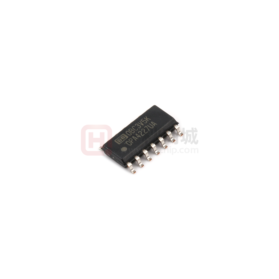


 工商网监
湘ICP备2023018690号
工商网监
湘ICP备2023018690号

