Sample &
Buy
Product
Folder
Support &
Community
Tools &
Software
Technical
Documents
Reference
Design
OPA376, OPA2376, OPA4376
SBOS406G – JUNE 2007 – REVISED DECEMBER 2015
OPAx376 Low-Noise, Low Quiescent Current, Precision Operational Amplifier
e-trim Series
1 Features
3 Description
•
•
•
•
•
•
•
•
•
The OPA376 family represents a new generation of
low-noise operational amplifiers with e-trim™, offering
outstanding dc precision and ac performance. Rail-torail input and output, low offset (25 μV, maximum),
low noise (7.5 nV/√Hz), quiescent current of 950 μA
(maximum), and a 5.5-MHz bandwidth make this part
very attractive for a variety of precision and portable
applications. In addition, this device has a reasonably
wide supply range with excellent PSRR, making it
attractive for applications that run directly from
batteries without regulation.
1
Low Noise: 7.5 nV/√Hz at 1 kHz
0.1 Hz to 10 Hz Noise: 0.8 μVPP
Quiescent Current: 760 μA (typical)
Low Offset Voltage: 5 μV (typ)
Gain Bandwidth Product: 5.5 MHz
Rail-to-Rail Input and Output
Single-Supply Operation
Supply Voltage: 2.2 V to 5.5 V
Space-Saving Packages:
– SC70, SOT-23, DSBGA, VSSOP, TSSOP
The OPA376 (single version) is available in
MicroSIZE SC70-5, SOT-23-5, and SOIC-8
packages. The OPA2376 (dual) is offered in the
DSBGA-8, VSSOP-8, and SOIC-8 packages. The
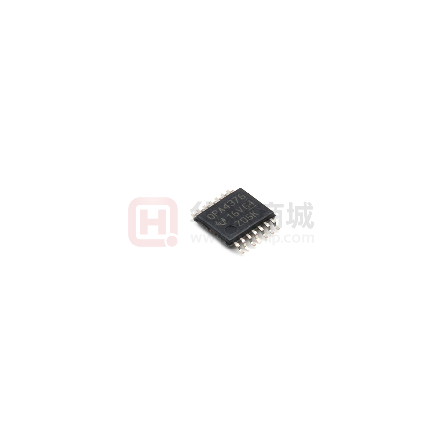
OPA4376 (quad) is offered in a TSSOP-14 package.
All versions are specified for operation from –40°C to
+125°C.
2 Applications
•
•
•
•
•
•
ADC Buffer
Audio Equipment
Medical Instrumentation
Handheld Test Equipment
Active Filtering
Sensor Signal Conditioning
Device Information(1)
PART NUMBER
OPA376
OPA2376
OPA4376
PACKAGE
BODY SIZE (NOM)
SOIC (8)
4.90 mm × 3.91 mm
SOT-23 (5)
2.90 mm × 1.60 mm
SC70 (5)
2.00 mm × 1.25 mm
SOIC (8)
4.90 mm × 3.91 mm
VSSOP (8)
3.00 mm × 3.00 mm
DSBGA (8)
1.30 mm × 2.30 mm
TSSOP (14)
5.00 mm × 4.40 mm
(1) For all available packages, see the package option addendum
at the end of the data sheet.
Input Noise Voltage Spectral Density
Offset Voltage Production Distribution
Population
10
1
1
10
100
1k
Frequency (Hz)
10k
100k
-25.0
-22.5
-20.0
-17.5
-15.0
-12.5
-10.0
-7.5
-5.0
-2.5
0
2.5
5.0
7.5
10.0
12.5
15.0
17.5
20.0
22.5
25.0
Voltage Noise (nV/ÖHz)
100
Offset Voltage (mV)
1
An IMPORTANT NOTICE at the end of this data sheet addresses availability, warranty, changes, use in safety-critical applications,
intellectual property matters and other important disclaimers. PRODUCTION DATA.
�OPA376, OPA2376, OPA4376
SBOS406G – JUNE 2007 – REVISED DECEMBER 2015
www.ti.com
Table of Contents
1
2
3
4
5
6
Features ..................................................................
Applications ...........................................................
Description .............................................................
Revision History.....................................................
Pin Configuration and Functions .........................
Specifications.........................................................
6.1
6.2
6.3
6.4
6.5
6.6
6.7
6.8
7
1
1
1
2
3
6
Absolute Maximum Ratings ...................................... 6
ESD Ratings.............................................................. 6
Recommended Operating Conditions....................... 6
Thermal Information: OPA376 .................................. 7
Thermal Information: OPA2376 ................................ 7
Thermal Information: OPA4376 ................................ 7
Electrical Characteristics.......................................... 8
Typical Characteristics ............................................ 10
Detailed Description ............................................ 14
7.1 Overview ................................................................. 14
7.2 Functional Block Diagram ....................................... 14
7.3 Feature Description................................................. 14
7.4 Device Functional Modes........................................ 16
8
Application and Implementation ........................ 17
8.1 Application Information............................................ 17
8.2 Typical Application ................................................. 20
9 Power Supply Recommendations...................... 21
10 Layout................................................................... 21
10.1 Layout Guidelines ................................................. 21
10.2 Layout Example .................................................... 22
11 Device and Documentation Support ................. 23
11.1
11.2
11.3
11.4
11.5
11.6
11.7
Device Support......................................................
Related Documentation .......................................
Related Links ........................................................
Community Resources..........................................
Trademarks ...........................................................
Electrostatic Discharge Caution ............................
Glossary ................................................................
23
23
24
24
24
24
24
12 Mechanical, Packaging, and Orderable
Information ........................................................... 25
4 Revision History
NOTE: Page numbers for previous revisions may differ from page numbers in the current version.
Changes from Revision F (March 2013) to Revision G
Page
•
Added ESD Ratings, Thermal Information, Recommended Operating Conditions, Power Supply Recommendations,
and Device and Documentation Support sections; existing sections may have moved ........................................................ 1
•
Changed WCSP to DSBGA and MSOP to VSSOP throughout data sheet ........................................................................... 1
•
Changed dimensions shown in YZD package pinout figure................................................................................................... 4
Changes from Revision E (January 2013) to Revision F
Page
•
Changed unit (typo) for Quiescent Current feature bullet....................................................................................................... 1
•
Changed TSSOP-14 pinout for OPA4376 .............................................................................................................................. 5
Changes from Revision D (August 2010) to Revision E
Page
•
Changed rail-to-rail feature bullet to show input and output................................................................................................... 1
•
Changed description text to show rail-to-rail input and output ............................................................................................... 1
Changes from Revision C (October 2008) to Revision D
Page
•
Updated format of Electrical Characteristics table ................................................................................................................. 8
•
Updated Figure 11................................................................................................................................................................ 11
2
Submit Documentation Feedback
Copyright © 2007–2015, Texas Instruments Incorporated
Product Folder Links: OPA376 OPA2376 OPA4376
�OPA376, OPA2376, OPA4376
www.ti.com
SBOS406G – JUNE 2007 – REVISED DECEMBER 2015
5 Pin Configuration and Functions
OPA376: DBV Package
5-Pin SOT23
Top View
OUT
1
V-
2
+IN
3
OPA376: DCK Package
5-Pin SC70-5
Top View
V+
5
4
+IN
1
V-
2
-IN
3
-IN
5
V+
4
OUT
OPA376: D Package
8-Pin SOIC
Top View
NC
(1)
(1)
1
8
NC
7
V+
(1)
-IN
2
+IN
3
6
OUT
V-
4
5
NC
+
(1)
NC denotes no internal connection.
Pin Functions: OPA376
PIN
NAME
I/O
DESCRIPTION
DBV
DCK
D
+IN
3
1
3
I
Input signal +
–IN
4
3
2
I
Input signal –
NC
—
—
1, 5, 8
—
No connection
OUT
1
4
6
O
Output signal
V+
5
5
7
—
Supply voltage+
V–
2
2
4
—
Supply voltage–
Copyright © 2007–2015, Texas Instruments Incorporated
Product Folder Links: OPA376 OPA2376 OPA4376
Submit Documentation Feedback
3
�OPA376, OPA2376, OPA4376
SBOS406G – JUNE 2007 – REVISED DECEMBER 2015
www.ti.com
OPA2376: D and DGK Packages
8-Pin SOIC and 8-Pin VSSOP
Top View
OPA2376: YZD Package
8-Pin DSBGA
Top View
OUT A
1
8
V+
-IN A
2
7
OUT B
+IN A
3
6
-IN B
V-
4
5
+IN B
+IN B
D2
D1
V-
-IN B
C2
C1
+IN A 2.178 mm
OUT B
B2
B1
-IN A 2.118 mm
V+
A2
A1
OUT A
1.14 mm
1.08 mm
(Bump-Side Down)
Pin Functions: OPA2376
PIN
I/O
DESCRIPTION
NAME
D AND
DGK
YZD
+IN A
3
C1
I
Input signal A+
–IN A
2
B1
I
Input signal A–
+IN B
5
D2
I
Input signal B+
–IN B
6
C2
I
Input signal B–
OUT A
1
A1
O
Output signal A
OUT B
7
B2
O
Output signal B
V+
8
A2
—
Supply voltage+
–
4
D1
—
Supply voltage–
V
4
Submit Documentation Feedback
Copyright © 2007–2015, Texas Instruments Incorporated
Product Folder Links: OPA376 OPA2376 OPA4376
�OPA376, OPA2376, OPA4376
www.ti.com
SBOS406G – JUNE 2007 – REVISED DECEMBER 2015
OPA4376: PW Package
14-Pin TSSOP
Top View
OUT A
1
14
OUT D
-IN A
2
13
-IN D
+IN A
3
12
+IN D
V+
4
11
V-
+IN B
5
10
+IN C
-IN B
6
9
-IN C
OUT B
7
8
OUT C
Pin Functions: OPA4376
PIN
I/O
DESCRIPTION
NAME
PW
+IN A
3
I
Input signal A+
–IN A
2
O
Input signal A–
+IN B
5
I
Input signal B+
–IN B
6
O
Input signal B–
+IN C
10
I
Input signal C+
–IN C
9
O
Input signal C–
+IN D
12
I
Input signal D+
–IN D
13
O
Input signal D–
OUT A
1
O
Output signal A
OUT B
7
O
Output signal B
OUT C
8
O
Output signal C
OUT D
14
O
Output signal D
V+
4
—
Supply voltage+
V–
11
—
Supply voltage–
Copyright © 2007–2015, Texas Instruments Incorporated
Product Folder Links: OPA376 OPA2376 OPA4376
Submit Documentation Feedback
5
�OPA376, OPA2376, OPA4376
SBOS406G – JUNE 2007 – REVISED DECEMBER 2015
www.ti.com
6 Specifications
6.1 Absolute Maximum Ratings
over operating free-air temperature range (unless otherwise noted) (1)
MIN
Voltage
Signal input pin
7
(2)
–
(V ) + 0.5
V
10
mA
Continuous
Operating range, TA
–40
(2)
(3)
150
Junction, TJ
150
Storage, Tstg
(1)
V
+
–10
Output short-circuit (3)
Temperature
UNIT
(V ) – 0.5
Signal input pin (2)
Current
MAX
Supply, VS = (V+) – (V–)
–65
°C
150
Stresses beyond those listed under Absolute Maximum Ratings may cause permanent damage to the device. These are stress ratings
only, which do not imply functional operation of the device at these or any other conditions beyond those indicated under Recommended
Operating Conditions. Exposure to absolute-maximum-rated conditions for extended periods may affect device reliability.
Input terminals are diode-clamped to the power-supply rails. Input signals that can swing more than 0.5 V beyond the supply rails should
be current limited to 10 mA or less.
Short-circuit to ground, one amplifier per package.
6.2 ESD Ratings
VALUE
V(ESD)
(1)
(2)
Electrostatic discharge
Human body model (HBM), per ANSI/ESDA/JEDEC JS-001,
all pins (1)
±4000
Charged device model (CDM), per JEDEC specification
JESD22-C101, all pins (2)
±1000
Machine model
±200
UNIT
V
JEDEC document JEP155 states that 500-V HBM allows safe manufacturing with a standard ESD control process.
JEDEC document JEP157 states that 250-V CDM allows safe manufacturing with a standard ESD control process.
6.3 Recommended Operating Conditions
over operating free-air temperature range (unless otherwise noted)
MIN
(V+) – (V–)
Supply voltage
TA
Operating temperature
6
Submit Documentation Feedback
NOM
MAX
UNIT
2.2 (±1.1)
5.5 (±2.75)
V
–40
150
°C
Copyright © 2007–2015, Texas Instruments Incorporated
Product Folder Links: OPA376 OPA2376 OPA4376
�OPA376, OPA2376, OPA4376
www.ti.com
SBOS406G – JUNE 2007 – REVISED DECEMBER 2015
6.4 Thermal Information: OPA376
OPA376
THERMAL METRIC (1)
DBV (SOT-23)
DCK (SC70)
D (SOIC)
5 PINS
5 PINS
8 PINS
UNIT
RθJA
Junction-to-ambient thermal resistance
273.8
267.0
100.1
°C/W
RθJC(top)
Junction-to-case (top) thermal resistance
126.8
80.9
42.4
°C/W
RθJB
Junction-to-board thermal resistance
85.9
54.8
41.0
°C/W
ψJT
Junction-to-top characterization parameter
10.9
1.2
4.8
°C/W
ψJB
Junction-to-board characterization parameter
84.9
54.1
40.3
°C/W
RθJC(bot)
Junction-to-case (bottom) thermal resistance
n/a
n/a
n/a
°C/W
(1)
For more information about traditional and new thermal metrics, see the Semiconductor and IC Package Thermal Metrics application
report, SPRA953.
6.5 Thermal Information: OPA2376
OPA2376
THERMAL METRIC
(1)
D (SOIC)
DGK (VSSOP)
YZD (DSBGA)
8 PINS
8 PINS
8 PINS
UNIT
119.2
°C/W
RθJA
Junction-to-ambient thermal resistance
111.1
171.2
RθJC(top)
Junction-to-case (top) thermal resistance
54.7
63.9
0.6
°C/W
RθJB
Junction-to-board thermal resistance
51.7
92.8
27.6
°C/W
ψJT
Junction-to-top characterization parameter
10.5
9.2
4.0
°C/W
ψJB
Junction-to-board characterization parameter
51.2
91.2
27.6
°C/W
RθJC(bot)
Junction-to-case (bottom) thermal resistance
n/a
n/a
n/a
°C/W
(1)
For more information about traditional and new thermal metrics, see theSemiconductor and IC Package Thermal Metrics application
report, SPRA953.
6.6 Thermal Information: OPA4376
OPA4376
THERMAL METRIC
(1)
PW
UNIT
14 PINS
RθJA
Junction-to-ambient thermal resistance
107.8
°C/W
RθJC(top)
Junction-to-case (top) thermal resistance
29.6
°C/W
RθJB
Junction-to-board thermal resistance
52.6
°C/W
ψJT
Junction-to-top characterization parameter
1.5
°C/W
ψJB
Junction-to-board characterization parameter
51.6
°C/W
RθJC(bot)
Junction-to-case (bottom) thermal resistance
n/a
°C/W
(1)
For more information about traditional and new thermal metrics, see theSemiconductor and IC Package Thermal Metrics application
report, SPRA953.
Copyright © 2007–2015, Texas Instruments Incorporated
Product Folder Links: OPA376 OPA2376 OPA4376
Submit Documentation Feedback
7
�OPA376, OPA2376, OPA4376
SBOS406G – JUNE 2007 – REVISED DECEMBER 2015
6.7
www.ti.com
Electrical Characteristics
At TA = 25°C, RL = 10 kΩ connected to VS / 2, VCM = VS / 2, and VOUT = VS / 2, unless otherwise noted.
PARAMETER
TEST CONDITIONS
MIN
TYP
MAX
UNIT
OFFSET VOLTAGE
VOS
dVOS/dT
PSRR
5
25
μV
TA = –40°C to +85°C
0.26
1
μV/°C
TA = –40°C to +125°C
Input offset voltage
Input offset voltage versus
temperature
Input offset voltage versus
power supply
0.32
2
μV/°C
TA = 25°C, VS = 2.2 V to 5.5 V, VCM < (V+) – 1.3 V
5
20
μV/V
TA = –40°C to +125°C,
VS = 2.2 V to 5.5 V, VCM < (V+) – 1.3 V
5
μV/V
0.5
mV/V
Channel separation, dc
(dual, quad)
INPUT BIAS CURRENT
IB
Input bias current
IOS
Input offset current
TA = 25°C
0.2
TA = –40°C to +125°C
10
See Typical Characteristics
0.2
pA
pA
10
pA
NOISE
Input voltage noise
f = 0.1 Hz to 10 Hz
0.8
μVPP
en
Input voltage noise density
f = 1 kHz
7.5
nV/√Hz
in
Input current noise
f = 1 kHz
2
fA/√Hz
INPUT VOLTAGE RANGE
VCM
Common-mode voltage
range
CMRR
Common-mode rejection
ratio
(V–) – 0.1
(V–) < VCM < (V+) – 1.3 V
76
(V+) + 0.1
V
90
dB
Differential
6.5
pF
Common-mode
13
pF
INPUT CAPACITANCE
OPEN-LOOP GAIN
AOL
Open-loop voltage gain
50 mV < VO < (V+) – 50 mV, RL = 10 kΩ
120
134
dB
100 mV < VO < (V+) – 100 mV, RL = 2 kΩ
120
126
dB
5.5
MHz
2
V/μs
FREQUENCY RESPONSE CL = 100 pF, VS = 5.5 V
GBW
Gain-bandwidth product
SR
Slew rate
tS
THD+N
8
Settling time
G=1
To 0.1%, 2-V step , G = 1
To 0.01%, 2-V step , G = 1
Overload recovery time
VIN × gain > VS
Total harmonic distortion +
noise
VO = 1 VRMS, G = 1, f = 1 kHz, RL = 10 kΩ
Submit Documentation Feedback
1.6
μs
2
μs
0.33
μs
0.00027%
Copyright © 2007–2015, Texas Instruments Incorporated
Product Folder Links: OPA376 OPA2376 OPA4376
�OPA376, OPA2376, OPA4376
www.ti.com
SBOS406G – JUNE 2007 – REVISED DECEMBER 2015
Electrical Characteristics (continued)
At TA = 25°C, RL = 10 kΩ connected to VS / 2, VCM = VS / 2, and VOUT = VS / 2, unless otherwise noted.
PARAMETER
TEST CONDITIONS
MIN
TYP
MAX
UNIT
SC70-5, SOT23-5, SO-8,
VSSOP-8, and TSSOP-14
packages only
10
20
mV
DSBGA package only
20
30
mV
40
mV
OUTPUT
TA = 25°C, RL = 10 kΩ
Voltage output swing from
rail
TA = –40°C to +125°C, RL = 10 kΩ
TA = 25°C, RL = 2 kΩ
SC70-5, SOT23-5, SO-8,
VSSOP-8, and TSSOP-14
packages only
40
50
mV
DSBGA package only
50
60
mV
80
mV
TA = –40°C to +125°C, RL = 2 kΩ
ISC
Short-circuit current
CLOAD
Capacitive load drive
RO
Open-loop output
impedance
+30, –50
mA
See Typical Characteristics
Ω
150
POWER SUPPLY
VS
Specified voltage range
2.2
Operating voltage range
IQ
Quiescent current per
amplifier
5.5
V
950
μA
1
mA
2 to 5.5
TA = 25°C, IO = 0, VS = 5.5 V, VCM < (V+) – 1.3 V
760
TA = –40°C to +125°C
V
TEMPERATURE
Specified range
–40
125
°C
Operating range
–40
150
°C
Copyright © 2007–2015, Texas Instruments Incorporated
Product Folder Links: OPA376 OPA2376 OPA4376
Submit Documentation Feedback
9
�OPA376, OPA2376, OPA4376
SBOS406G – JUNE 2007 – REVISED DECEMBER 2015
www.ti.com
6.8 Typical Characteristics
0
140
-20
120
-40
Gain
100
-60
Phase
80
-80
60
-100
40
-120
20
-140
0
-160
-20
0.1
1
10
100
120
1k
10k
100k
1M
Power-Supply Rejection Ratio (dB)
160
Phase Margin (°)
Open-Loop Gain (dB)
At TA = 25°C, VS = 5 V, RL = 10 kΩ connected to VS / 2, VCM = VS / 2, and VOUT = VS / 2, unless otherwise noted.
V(+) Power-Supply Rejection Ratio
100
80
Common-Mode
Rejection Ratio
60
40
V(-) Power-Supply Rejection Ratio
20
0
-180
10M
100
10
1k
10k
100k
1M
10M
Frequency (Hz)
Frequency (Hz)
Figure 2. Power-Supply and Common-Mode Rejection Ratio
vs Frequency
Figure 1. Open-Loop Gain and Phase vs Frequency
Open-Loop Gain (RL = 2kW)
140
120
500nV/div
Open-Loop Gain and PSRR (dB)
160
Power-Supply Rejection Ratio
(VS = 2.1V to 5.5V)
100
80
-50
0
-25
25
50
75
100
125
150
Temperature (°C)
1s/div
Figure 3. Open-Loop Gain and Power-Supply Rejection
Ratio vs Temperature
Figure 4. 0.1-Hz to 10-Hz Input Voltage Noise
1
Total Harmonic Distortion + Noise (%)
Voltage Noise (nV/ÖHz)
100
10
1
VS = 5V, VCM = 2V, VOUT = 1VRMS
0.1
0.01
Gain = 10V/V
0.001
Gain = 1V/V
0.0001
1
10
100
1k
10k
100k
10
100
Frequency (Hz)
Figure 5. Input Voltage Noise Spectral Density
10
Submit Documentation Feedback
1k
10k
100k
Frequency (Hz)
Figure 6. Total Harmonic Distortion + Noise vs Frequency
Copyright © 2007–2015, Texas Instruments Incorporated
Product Folder Links: OPA376 OPA2376 OPA4376
�OPA376, OPA2376, OPA4376
www.ti.com
SBOS406G – JUNE 2007 – REVISED DECEMBER 2015
Typical Characteristics (continued)
At TA = 25°C, VS = 5 V, RL = 10 kΩ connected to VS / 2, VCM = VS / 2, and VOUT = VS / 2, unless otherwise noted.
1000
100
900
Quiescent Current (mA)
Common-Mode Rejection Ratio (dB)
110
90
80
70
800
700
600
60
50
500
-50
-25
0
25
50
75
100
125
150
-50
-25
0
Temperature (°C)
25
50
75
100
125
150
Temperature (°C)
Figure 7. Common-Mode Rejection Ratio vs Temperature
Figure 8. Quiescent Current vs Temperature
75
50
1000
VS = ±2.75V
Quiescent Current (mA)
ISC+
30
800
IQ
700
20
10
600
Short-Circuit Current (mA)
40
900
0
500
2.0
2.5
3.0
3.5
4.0
4.5
5.0
Short-Circuit Current (mA)
50
ISC+
25
0
-25
ISC-
-50
-75
-100
-50
5.5
-25
0
25
50
75
100
Supply Voltage (V)
150
Figure 10. Short-Circuit Current vs Temperature
Figure 9. Quiescent and Short-Circuit Current vs Supply
Voltage
3
1000
VS = ±2.75
900
2
800
Output Voltage (V)
Input Bias Current (pA)
125
Temperature (°C)
700
600
500
400
300
200
1
+150°C
+125°C
+25°C
-40°C
0
-1
-2
100
-3
0
-50
-25
0
25
50
75
100
125
150
0
10
20
Figure 11. Input Bias Current vs Temperature
30
40
50
60
70
80
Output Current (mA)
Temperature (°C)
Figure 12. Output Voltage vs Output Current
Copyright © 2007–2015, Texas Instruments Incorporated
Product Folder Links: OPA376 OPA2376 OPA4376
Submit Documentation Feedback
11
�OPA376, OPA2376, OPA4376
SBOS406G – JUNE 2007 – REVISED DECEMBER 2015
www.ti.com
Typical Characteristics (continued)
-25.0
-22.5
-20.0
-17.5
-15.0
-12.5
-10.0
-7.5
-5.0
-2.5
0
2.5
5.0
7.5
10.0
12.5
15.0
17.5
20.0
22.5
25.0
0
0.1
0.2
0.3
0.4
0.5
0.6
0.7
0.8
0.9
1.0
1.1
1.2
1.3
1.4
1.5
1.6
1.7
1.8
1.9
2.0
Population
Population
At TA = 25°C, VS = 5 V, RL = 10 kΩ connected to VS / 2, VCM = VS / 2, and VOUT = VS / 2, unless otherwise noted.
Offset Voltage (mV)
½Offset Voltage Drift½ (mV/°C)
Figure 14. Offset Voltage Drift Production Distribution
(–40°C to 125°C)
Figure 13. Offset Voltage Production Distribution
6
G = +1V/V
Small-Signal Overshoot (%)
5
Output Voltage (VPP)
50
VS = 5.5V
VS = 5V
4
3
VS = 2.5V
2
1
40
30
20
10
0
0
1k
10k
100k
1M
10M
10
100
Frequency (Hz)
Figure 15. Maximum Output Voltage vs Frequency
Figure 16. Small-Signal Overshoot vs Load Capacitance
G = +1
RL = 2kW
CL = 50pF
1V/div
50mV/div
G = +1
RL = 10kW
CL = 50pF
Time (2ms/div)
Time (400ns/div)
Figure 17. Small-Signal Pulse Response
12
1k
Load Capacitance (pF)
Submit Documentation Feedback
Figure 18. Large-Signal Pulse Response
Copyright © 2007–2015, Texas Instruments Incorporated
Product Folder Links: OPA376 OPA2376 OPA4376
�OPA376, OPA2376, OPA4376
www.ti.com
SBOS406G – JUNE 2007 – REVISED DECEMBER 2015
Typical Characteristics (continued)
At TA = 25°C, VS = 5 V, RL = 10 kΩ connected to VS / 2, VCM = VS / 2, and VOUT = VS / 2, unless otherwise noted.
140
100
Channel Separation (dB)
Settling Time (ms)
120
10
0.01%
1
0.1%
100
80
60
40
20
0
0.1
1
10
10
100
100
10k
1k
100k
1M
10M
100M
Closed-Loop Gain (V/V)
Frequency (Hz)
Figure 19. Settling Time vs Closed-Loop Gain
Figure 20. Channel Separation vs Frequency
Open-Loop Output Resistance (W)
1k
100
10
400mA Load
2mA Load
1
0.1
10
100
1k
10k
100k
1M
10M
Frequency (Hz)
Figure 21. Open-Loop Output Resistance vs Frequency
Copyright © 2007–2015, Texas Instruments Incorporated
Product Folder Links: OPA376 OPA2376 OPA4376
Submit Documentation Feedback
13
�OPA376, OPA2376, OPA4376
SBOS406G – JUNE 2007 – REVISED DECEMBER 2015
www.ti.com
7 Detailed Description
7.1 Overview
The OPA376 family belongs to a new generation of low-noise operational amplifiers with e-trim, giving customers
outstanding dc precision and ac performance. Low noise, rail-to-rail input and output, and low offset, drawing a
low quiescent current, make these devices ideal for a variety of precision and portable applications. In addition,
this device has a wide supply range with excellent PSRR, making it a suitable option for applications that are
battery-powered without regulation.
7.2 Functional Block Diagram
V+
OPAx376
-IN
OUT
+IN
POR
e-trim
V-
7.3 Feature Description
The OPAx376 family of precision amplifiers offers excellent dc performance as well as excellent ac performance.
Operating from a single power-supply the OPAx376 is capable of driving large capacitive loads, has a wide input
common-mode voltage range, and is well-suited to drive the inputs of SAR ADCs as well as 24-bit and higher
resolution converters. Including internal ESD protection, the OPAx376 family is offered in a variety of industrystandard packages, including a wafer chip-scale package for applications that require space savings.
7.3.1 Operating Voltage
The OPA376 family of amplifiers operates over a power-supply range of 2.2 V to 5.5 V (±1.1 V to ±2.75 V). Many
of the specifications apply from –40°C to +125°C. Parameters that can exhibit significant variance with regard to
operating voltage or temperature are presented in the Typical Characteristics.
7.3.2 Input Offset Voltage and Input Offset Voltage Drift
The OPAx376 family of operational amplifiers is manufactured using TI's e-trim technology. Each amplifier is
trimmed in production, thereby minimizing errors associated with input offset voltage and input offset voltage drift.
The e-trim technology is a TI proprietary method of trimming internal device parameters during either wafer
probing or final testing.
7.3.3 Capacitive Load and Stability
The OPA376 series of amplifiers may be used in applications where driving a capacitive load is required. As with
all op amps, there may be specific instances where the OPAx376 can become unstable, leading to oscillation.
The particular op amp circuit configuration, layout, gain, and output loading are some of the factors to consider
when establishing whether an amplifier will be stable in operation. An op amp in the unity-gain (+1-V/V) buffer
configuration and driving a capacitive load exhibits a greater tendency to be unstable than an amplifier operated
at a higher noise gain. The capacitive load, in conjunction with the op amp output resistance, creates a pole
within the feedback loop that degrades the phase margin. The degradation of the phase margin increases as the
capacitive loading increases.
14
Submit Documentation Feedback
Copyright © 2007–2015, Texas Instruments Incorporated
Product Folder Links: OPA376 OPA2376 OPA4376
�OPA376, OPA2376, OPA4376
www.ti.com
SBOS406G – JUNE 2007 – REVISED DECEMBER 2015
Feature Description (continued)
The OPAx376 in a unity-gain configuration can directly drive up to 250 pF of pure capacitive load. Increasing the
gain enhances the ability of the amplifier to drive greater capacitive loads; see the typical characteristic
Figure 16. In unity-gain configurations, capacitive load drive can be improved by inserting a small (10-Ω to 20-Ω)
resistor, RS, in series with the output, as shown in Figure 22. This resistor significantly reduces ringing while
maintaining dc performance for purely capacitive loads. However, if there is a resistive load in parallel with the
capacitive load, a voltage divider is created, introducing a gain error at the output and slightly reducing the output
swing. The error introduced is proportional to the ratio RS / RL, and is generally negligible at low output current
levels.
V+
RS
VOUT
OPA376
10W to
20W
VIN
RL
CL
Figure 22. Improving Capacitive Load Drive
7.3.4 Common-Mode Voltage Range
The input common-mode voltage range of the OPA376 series extends 100 mV beyond the supply rails. The
offset voltage of the amplifier is very low, from approximately (V–) to (V+) – 1 V, as shown in Figure 23. The offset
voltage increases as common-mode voltage exceeds (V+) –1 V. Common-mode rejection is specified from (V–) to
(V+) – 1.3 V.
Input Offset Voltage (mV)
3
2
1
0
-1
-2
-V
+V
-3
-0.5 0
0.5 1.0 1.5 2.0 2.5 3.0 3.5 4.0 4.5 5.0 5.5 6.0
Input Common-Mode Voltage (V)
Figure 23. Offset and Common-Mode Voltage
Copyright © 2007–2015, Texas Instruments Incorporated
Product Folder Links: OPA376 OPA2376 OPA4376
Submit Documentation Feedback
15
�OPA376, OPA2376, OPA4376
SBOS406G – JUNE 2007 – REVISED DECEMBER 2015
www.ti.com
Feature Description (continued)
7.3.5 Input and ESD Protection
The OPA376 family incorporates internal electrostatic discharge (ESD) protection circuits on all pins. In the case
of input and output pins, this protection primarily consists of current steering diodes connected between the input
and power-supply pins. These ESD protection diodes also provide in-circuit, input overdrive protection, as long
as the current is limited to 10 mA as stated in the Absolute Maximum Ratings. Figure 24 shows how a series
input resistor may be added to the driven input to limit the input current. The added resistor contributes thermal
noise at the amplifier input and its value should be kept to a minimum in noise-sensitive applications.
V+
IOVERLOAD
10mA max
OPA376
VOUT
VIN
5kW
Figure 24. Input Current Protection
7.4 Device Functional Modes
The OPAx376 has a single functional mode and is operational when the power-supply voltage is greater than
2.2 V (±1.1 V). The maximum power supply voltage for the OPAx376 is 5.5 V (±2.75 V).
16
Submit Documentation Feedback
Copyright © 2007–2015, Texas Instruments Incorporated
Product Folder Links: OPA376 OPA2376 OPA4376
�OPA376, OPA2376, OPA4376
www.ti.com
SBOS406G – JUNE 2007 – REVISED DECEMBER 2015
8 Application and Implementation
NOTE
Information in the following applications sections is not part of the TI component
specification, and TI does not warrant its accuracy or completeness. TI’s customers are
responsible for determining suitability of components for their purposes. Customers should
validate and test their design implementation to confirm system functionality.
8.1 Application Information
The OPA376 family of operational amplifiers is built using e-trim, a proprietary technique in which offset voltage
is adjusted during the final steps of manufacturing. This technique compensates for performance shifts that can
occur during the molding process. Through e-trim, the OPA376 family delivers excellent offset voltage (5 μV,
typical). Additionally, the amplifier boasts a fast slew rate, low drift, low noise, and excellent PSRR and AOL.
These 5.5-MHz CMOS op amps operate on 760-μA (typical) quiescent current.
8.1.1 Basic Amplifier Configurations
The OPA376 family is unity-gain stable. It does not exhibit output phase inversion when the input is overdriven. A
typical single-supply connection is shown in Figure 25. The OPA376 is configured as a basic inverting amplifier
with a gain of –10 V/V. This single-supply connection has an output centered on the common-mode voltage, VCM.
For the circuit shown, this voltage is 2.5 V, but may be any value within the common-mode input voltage range.
R2
10kW
+5V
C1
100nF
R1
1kW
OPA376
VOUT
VIN
VCM = 2.5V
Figure 25. Basic Single-Supply Connection
Copyright © 2007–2015, Texas Instruments Incorporated
Product Folder Links: OPA376 OPA2376 OPA4376
Submit Documentation Feedback
17
�OPA376, OPA2376, OPA4376
SBOS406G – JUNE 2007 – REVISED DECEMBER 2015
www.ti.com
Application Information (continued)
8.1.2 Active Filtering
The OPA376 series is well-suited for filter applications requiring a wide bandwidth, fast slew rate, low-noise,
single-supply operational amplifier. Figure 26 shows a 50-kHz, 2nd-order, low-pass filter. The components have
been selected to provide a maximally-flat Butterworth response. Beyond the cutoff frequency, roll-off is
–40 dB/decade. The Butterworth response is ideal for applications requiring predictable gain characteristics such
as the anti-aliasing filter used ahead of an analog-to-digital converter (ADC).
R3
5.49kW
C2
150pF
V+
R1
5.49kW
R2
12.4kW
OPA376
VOUT
C1
1nF
VIN
(V+)/2
Figure 26. Second-Order, Butterworth, 50-kHz, Low-Pass Filter
8.1.3 Driving an Analog-to-Digital Converter
The low noise and wide gain bandwidth of the OPA376 family make it an ideal driver for ADCs. Figure 27
illustrates the OPA376 driving an ADS8327, a 16-bit, 250-kSPS converter. The amplifier is connected as a unitygain, non-inverting buffer.
+5V
C1
0.1mF
+5V
(1)
R1
100W
+IN
OPA376
(1)
C3
VIN
1.2nF
ADS8327
Low Power
16-Bit
500kSPS
-IN
REF IN
+5V
REF5040
4.096V
(1)
C4
100nF
Suggested value; may require adjustment based on specific application.
Figure 27. Driving an ADS8327
18
Submit Documentation Feedback
Copyright © 2007–2015, Texas Instruments Incorporated
Product Folder Links: OPA376 OPA2376 OPA4376
�OPA376, OPA2376, OPA4376
www.ti.com
SBOS406G – JUNE 2007 – REVISED DECEMBER 2015
Application Information (continued)
8.1.4 Phantom-Powered Microphone
The circuit shown in Figure 28 depicts how a remote microphone amplifier can be powered by a phantom source
on the output side of the signal cable. The cable serves double duty, carrying both the differential output signal
from and dc power to the microphone amplifier stage.
An OPA2376 serves as a single-ended input to a differential output amplifier with a 6-dB gain. Common-mode
bias for the two op amps is provided by the dc voltage developed across the electret microphone element. A
48-V phantom supply is reduced to 5.1 V by the series 6.8-kΩ resistors on the output side of the cable, and the
4.7-kΩ resistor and zener diode on the input side of the cable. AC coupling blocks the different dc voltage levels
from each other on each end of the cable.
An INA163 instrumentation amplifier provides differential inputs and receives the balanced audio signals from the
cable. The INA163 gain may be set from 0 dB to 80 dB by selecting the RG value. The INA163 circuit is typical of
the input circuitry used in mixing consoles.
Phantom Power
(Provides power source for microphone)
48V
Microphone
100W
+
1mF
+
D1
5.1V
33mF
R1
2.7kW
C2
33mF
R9
4.7kW
R8
4.7kW
R6
100W
R10
6.8kW
+
1/2
OPA2376
R11
6.8kW
+15V
10mF
+
2
2
3
3
1kW
RG
INA163
10mF
+
Panasonic
WM-034CY
1kW
1
10kW
+
1
R7
100W
3.3kW
+
1/2
OPA2376
C3
33mF
3.3kW
Low-level differential audio signal
is transmitted differentially on the
same cable as power to the microphone.
-15V
10mF
Typical microphone input circuit used in mixing consoles.
Figure 28. Phantom-Powered Electret Microphone
V+ = +2.7V to 5V
Passband 300Hz to 3kHz
R9
510kW
R1
1.5kW
R2
1MW
R4
20kW
C3
33pF
C1
1000pF
1/2
OPA2376
Electret
(1)
Microphone
R3
1MW
R6
100kW
R7
51kW
R8
150kW
VREF 1
8 V+
7
1/2
OPA2376
C2
1000pF
+IN
ADS7822 6
12-Bit A/D
5
2
-IN
DCLOCK
DOUT
CS/SHDN
Serial
Interface
3
4
R5
20kW
G = 100
GND
(1) Electret microphone powered by R1.
Figure 29. OPA2376 as a Speech Bandpass-Filtered, Data Acquisition System
Copyright © 2007–2015, Texas Instruments Incorporated
Product Folder Links: OPA376 OPA2376 OPA4376
Submit Documentation Feedback
19
�OPA376, OPA2376, OPA4376
SBOS406G – JUNE 2007 – REVISED DECEMBER 2015
www.ti.com
8.2 Typical Application
Low-pass filters are commonly employed in signal processing applications to reduce noise and prevent aliasing.
The OPA376 is ideally suited to construct high-speed, high-precision active filters. Figure 30 shows a secondorder, low-pass filter commonly encountered in signal processing applications.
R4
2.94 k
C5
1 nF
R1
590
R3
499
Input
C2
39 nF
±
Output
+
OPA376
Figure 30. Typical Application Schematic
8.2.1 Design Requirements
Use the following parameters for this design example:
• Gain = 5 V/V (inverting gain)
• Low-pass cutoff frequency = 25 kHz
• Second-order Chebyshev filter response with 3-dB gain peaking in the passband
8.2.1.1 Detailed Design Procedure
The infinite-gain multiple-feedback circuit for a low-pass network function is shown in Figure 30. Use Equation 1
to calculate the voltage transfer function.
1 R1R3C2C5
Output
s
2
Input
s
s C2 1 R1 1 R3 1 R4 1 R3R4C2C5
(1)
This circuit produces a signal inversion. For this circuit, the gain at dc and the low-pass cutoff frequency are
calculated by Equation 2:
R4
Gain
R1
fC
1
2S
1 R3R 4 C2C5
(2)
Software tools are readily available to simplify filter design. WEBENCH® Filter Designer is a simple, powerful,
and easy-to-use active filter design program. The WEBENCH Filter Designer lets you create optimized filter
designs using a selection of TI operational amplifiers and passive components from TI's vendor partners.
Available as a web based tool from the WEBENCH® Design Center, WEBENCH® Filter Designer allows you to
design, optimize, and simulate complete multistage active filter solutions within minutes.
20
Submit Documentation Feedback
Copyright © 2007–2015, Texas Instruments Incorporated
Product Folder Links: OPA376 OPA2376 OPA4376
�OPA376, OPA2376, OPA4376
www.ti.com
SBOS406G – JUNE 2007 – REVISED DECEMBER 2015
Typical Application (continued)
8.2.2 Application Curve
20
Gain (db)
0
-20
-40
-60
100
1k
10k
Frequency (Hz)
100k
1M
Figure 31. Low-Pass Filter Transfer Function
9 Power Supply Recommendations
The OPAx376 are specified for operation from 2.2 V to 5.5 V (±1.1 V to ±2.75 V); many specifications apply from
–40°C to +125°C. Parameters that can exhibit significant variance with regard to operating voltage or
temperature are presented in the Typical Characteristics.
10 Layout
10.1 Layout Guidelines
For best operational performance of the device, use good PCB layout practices, including:
• Noise can propagate into analog circuitry through the power pins of the circuit as a whole, and the op
amp itself. Bypass capacitors can reduce the coupled noise by providing low-impedance power sources
local to the analog circuitry.
– Connect low-ESR, 0.1-µF ceramic bypass capacitors between each supply pin and ground, placed as
close to the device as possible. A single bypass capacitor from V+ to ground is applicable for singlesupply applications.
• Separate grounding for analog and digital portions of circuitry is one of the simplest and most effective
methods of noise suppression. One or more layers on multilayer PCBs are usually devoted to ground
planes. A ground plane helps distribute heat, and reduces EMI noise pickup. Physically separate the
digital and analog grounds, paying attention to the flow of the ground current. For more detailed
information refer to Circuit Board Layout Techniques, SLOA089.
• To reduce parasitic coupling, run the input traces as far away from the supply or output traces as
possible. If these traces cannot be kept separate, crossing the sensitive trace perpendicular is better than
opposed to in parallel with the noisy trace.
• Place the external components as close to the device as possible. As shown in Figure 32, keeping RF
and RG close to the inverting input minimizes parasitic capacitance.
• Keep the length of the input traces as short as possible. The input traces are the most sensitive part of
the circuit.
• Consider a driven, low-impedance guard ring around the critical traces. A guard ring can significantly
reduce leakage currents from nearby traces that are at different potentials.
• Clean the PCB following board assembly for best performance.
• Any precision-integrated circuit may experience performance shifts due to moisture ingress into the
plastic package. Following any aqueous PCB cleaning process, bake the PCB assembly to remove
moisture introduced into the device packaging during the cleaning process. A low-temperature, postcleaning bake at 85°C for 30 minutes is sufficient for most circumstances.
Copyright © 2007–2015, Texas Instruments Incorporated
Product Folder Links: OPA376 OPA2376 OPA4376
Submit Documentation Feedback
21
�OPA376, OPA2376, OPA4376
SBOS406G – JUNE 2007 – REVISED DECEMBER 2015
www.ti.com
Layout Guidelines (continued)
10.1.1 Photosensitivity
Although the OPA2376YZD package has a protective backside coating that reduces the amount of light exposure
on the die, unless fully shielded, ambient light can reach the active region of the device. Input bias current for the
package is specified in the absence of light. Depending on the amount of light exposure in a given application, an
increase in bias current, and possible increases in offset voltage, should be expected. Fluorescent lighting may
introduce noise or hum because of the time-varying light output. Best layout practices include end-product
packaging that provides shielding from possible light sources during operation.
10.2 Layout Example
+
VIN
VOUT
RG
RF
(Schematic Representation)
Run the input traces
as far away from
the supply lines
as possible
Place components
close to device and to
each other to reduce
parasitic errors
VS+
RF
N/C
N/C
GND
±IN
V+
VIN
+IN
OUTPUT
V±
N/C
RG
Use low-ESR,
ceramic bypass
capacitor
GND
VS±
GND
Use low-ESR, ceramic
bypass capacitor
VOUT
Ground (GND) plane on another layer
Figure 32. Layout Example
22
Submit Documentation Feedback
Copyright © 2007–2015, Texas Instruments Incorporated
Product Folder Links: OPA376 OPA2376 OPA4376
�OPA376, OPA2376, OPA4376
www.ti.com
SBOS406G – JUNE 2007 – REVISED DECEMBER 2015
11 Device and Documentation Support
11.1 Device Support
11.1.1 Development Support
11.1.1.1 TINA-TI™ (Free Software Download)
TINA™ is a simple, powerful, and easy-to-use circuit simulation program based on a SPICE engine. TINA-TI™ is
a free, fully-functional version of the TINA software, preloaded with a library of macro models in addition to a
range of both passive and active models. TINA-TI provides all the conventional dc, transient, and frequency
domain analysis of SPICE, as well as additional design capabilities.
Available as a free download from the Analog eLab Design Center, TINA-TI offers extensive post-processing
capability that allows users to format results in a variety of ways. Virtual instruments offer the ability to select
input waveforms and probe circuit nodes, voltages, and waveforms, creating a dynamic quick-start tool.
NOTE
These files require that either the TINA software (from DesignSoft™) or TINA-TI software
be installed. Download the free TINA-TI software from the TINA-TI folder.
11.1.1.2 TI Precision Designs
TI Precision Designs are analog solutions created by TI’s precision analog applications experts and offer the
theory of operation, component selection, simulation, complete PCB schematic and layout, bill of materials, and
measured performance of many useful circuits. TI Precision Designs are available online at
http://www.ti.com/ww/en/analog/precision-designs/.
11.1.1.3 WEBENCH® Filter Designer
WEBENCH® Filter Designer is a simple, powerful, and easy-to-use active filter design program. The WEBENCH
Filter Designer lets you create optimized filter designs using a selection of TI operational amplifiers and passive
components from TI's vendor partners.
Available as a web-based tool from the WEBENCH® Design Center, WEBENCH® Filter Designer allows you to
design, optimize, and simulate complete multistage active filter solutions within minutes.
11.2 Related Documentation
For related documentation, see the following:
Circuit Board Layout Techniques, SLOA089.
Operational Amplifier Gain stability, Part 3: AC Gain-Error Analysis, SLYT383.
Operational Amplifier Gain Stability, Part 2: DC Gain-Error Analysis, SLYT374.
Using infinite-gain, MFB filter topology in fully differential active filters, SLYT343.
Op Amp Performance Analysis, SBOS054.
Single-Supply Operation of Operational Amplifiers, SBOA059.
Tuning in Amplifiers, SBOA067.
Shelf-Life Evaluation of Lead-Free Component Finishes, SZZA046.
Copyright © 2007–2015, Texas Instruments Incorporated
Product Folder Links: OPA376 OPA2376 OPA4376
Submit Documentation Feedback
23
�OPA376, OPA2376, OPA4376
SBOS406G – JUNE 2007 – REVISED DECEMBER 2015
www.ti.com
11.3 Related Links
See Table 1 for a list of quick access links. Categories include technical documents, support and community
resources, tools and software, and quick access to sample or buy.
Table 1. Related Links
PARTS
PRODUCT FOLDER
SAMPLE AND BUY
TECHNICAL
DOCUMENTS
TOOLS AND
SOFTWARE
SUPPORT AND
COMMUNITY
OPA376
Click here
Click here
Click here
Click here
Click here
OPA2376
Click here
Click here
Click here
Click here
Click here
OPA4376
Click here
Click here
Click here
Click here
Click here
11.4 Community Resources
The following links connect to TI community resources. Linked contents are provided "AS IS" by the respective
contributors. They do not constitute TI specifications and do not necessarily reflect TI's views; see TI's Terms of
Use.
TI E2E™ Online Community TI's Engineer-to-Engineer (E2E) Community. Created to foster collaboration
among engineers. At e2e.ti.com, you can ask questions, share knowledge, explore ideas and help
solve problems with fellow engineers.
Design Support TI's Design Support Quickly find helpful E2E forums along with design support tools and
contact information for technical support.
11.5 Trademarks
e-trim, TINA-TI, E2E, NanoStar, NanoFree are trademarks of Texas Instruments.
TINA, DesignSoft are trademarks of DesignSoft, Inc.
All other trademarks are the property of their respective owners.
11.6 Electrostatic Discharge Caution
This integrated circuit can be damaged by ESD. Texas Instruments recommends that all integrated circuits be handled with
appropriate precautions. Failure to observe proper handling and installation procedures can cause damage.
ESD damage can range from subtle performance degradation to complete device failure. Precision integrated circuits may be more
susceptible to damage because very small parametric changes could cause the device not to meet its published specifications.
11.7 Glossary
SLYZ022 — TI Glossary.
This glossary lists and explains terms, acronyms, and definitions.
24
Submit Documentation Feedback
Copyright © 2007–2015, Texas Instruments Incorporated
Product Folder Links: OPA376 OPA2376 OPA4376
�OPA376, OPA2376, OPA4376
www.ti.com
SBOS406G – JUNE 2007 – REVISED DECEMBER 2015
12 Mechanical, Packaging, and Orderable Information
The following pages include mechanical, packaging, and orderable information. This information is the most
current data available for the designated devices. This data is subject to change without notice and revision of
this document. For browser-based versions of this data sheet, refer to the left-hand navigation.
The OPAx376 are specified for operation from 2.2 V to 5.5 V (±1.1 V to ±2.75 V); many specifications apply
from –40°C to +125°C. Parameters that can exhibit significant variance with regard to operating voltage or
temperature are presented in the Typical Characteristics.
The OPA2376YZD is a lead (Pb)-free, die-level, die-size ball grid array (DSBGA) package. Unlike devices that
are in plastic packages, these devices have no molding compound, lead frame, wire bonds, or leads. Using
standard surface-mount assembly procedures, the DSBGA can be mounted to a printed circuit board (PCB)
without additional underfill. Figure 33 and Figure 34 detail the pinout and package marking. See Application Note
SBVA017, NanoStar™ and NanoFree™ 300 μm Solder Bump WCSP, for more detailed information on package
characteristics and PCB design.
OPA2376YZD
WCSP-8 Enlarged Image
Top View
(bump side down)
OPA2376YZD
Top View
(bump side down)
Not to Scale
D2
D1
V-
-IN B
C2
C1
+IN A
OUT B
B2
B1
-IN A
V+
A2
A1
OUT A
Actual Size:
Exact Size:
1.150mm x 2.188mm
YMDCGLS
+IN B
Package Marking Code:
YMD = year/month/day
CGL = indicates OPA2376YZD
S = for engineering purposes only
Figure 34. Top-View Package Marking
WCSP-8
Figure 33. Pin Description
Copyright © 2007–2015, Texas Instruments Incorporated
Product Folder Links: OPA376 OPA2376 OPA4376
Submit Documentation Feedback
25
�PACKAGE OPTION ADDENDUM
www.ti.com
6-Feb-2020
PACKAGING INFORMATION
Orderable Device
Status
(1)
Package Type Package Pins Package
Drawing
Qty
Eco Plan
Lead/Ball Finish
MSL Peak Temp
(2)
(6)
(3)
Op Temp (°C)
Device Marking
(4/5)
OPA2376AID
ACTIVE
SOIC
D
8
75
Green (RoHS
& no Sb/Br)
NIPDAU
Level-2-260C-1 YEAR
-40 to 125
OPA
2376
OPA2376AIDGKR
ACTIVE
VSSOP
DGK
8
2500
Green (RoHS
& no Sb/Br)
NIPDAUAG
Level-2-260C-1 YEAR
-40 to 125
OBBI
OPA2376AIDGKRG4
ACTIVE
VSSOP
DGK
8
2500
Green (RoHS
& no Sb/Br)
NIPDAUAG
Level-2-260C-1 YEAR
-40 to 125
OBBI
OPA2376AIDGKT
ACTIVE
VSSOP
DGK
8
250
Green (RoHS
& no Sb/Br)
NIPDAUAG
Level-2-260C-1 YEAR
-40 to 125
OBBI
OPA2376AIDR
ACTIVE
SOIC
D
8
2500
Green (RoHS
& no Sb/Br)
NIPDAU
Level-2-260C-1 YEAR
-40 to 125
OPA
2376
OPA2376AIDRG4
ACTIVE
SOIC
D
8
2500
Green (RoHS
& no Sb/Br)
NIPDAU
Level-2-260C-1 YEAR
-40 to 125
OPA
2376
OPA2376AIYZDR
ACTIVE
DSBGA
YZD
8
3000
Green (RoHS
& no Sb/Br)
SNAGCU
Level-1-260C-UNLIM
-40 to 125
OPA2376
OPA2376AIYZDT
ACTIVE
DSBGA
YZD
8
250
Green (RoHS
& no Sb/Br)
SNAGCU
Level-1-260C-UNLIM
-40 to 125
OPA2376
OPA376AID
ACTIVE
SOIC
D
8
75
Green (RoHS
& no Sb/Br)
NIPDAU
Level-2-260C-1 YEAR
-40 to 125
OPA
376
OPA376AIDBVR
ACTIVE
SOT-23
DBV
5
3000
Green (RoHS
& no Sb/Br)
NIPDAU
Level-2-260C-1 YEAR
-40 to 125
BUQ
OPA376AIDBVRG4
ACTIVE
SOT-23
DBV
5
3000
Green (RoHS
& no Sb/Br)
NIPDAU
Level-2-260C-1 YEAR
-40 to 125
BUQ
OPA376AIDBVT
ACTIVE
SOT-23
DBV
5
250
Green (RoHS
& no Sb/Br)
NIPDAU
Level-2-260C-1 YEAR
-40 to 125
BUQ
OPA376AIDBVTG4
ACTIVE
SOT-23
DBV
5
250
Green (RoHS
& no Sb/Br)
NIPDAU
Level-2-260C-1 YEAR
-40 to 125
BUQ
OPA376AIDCKR
ACTIVE
SC70
DCK
5
3000
Green (RoHS
& no Sb/Br)
NIPDAU
Level-2-260C-1 YEAR
-40 to 125
BUR
OPA376AIDCKRG4
ACTIVE
SC70
DCK
5
3000
Green (RoHS
& no Sb/Br)
NIPDAU
Level-2-260C-1 YEAR
-40 to 125
BUR
OPA376AIDCKT
ACTIVE
SC70
DCK
5
250
Green (RoHS
& no Sb/Br)
NIPDAU
Level-2-260C-1 YEAR
-40 to 125
BUR
OPA376AIDCKTG4
ACTIVE
SC70
DCK
5
250
Green (RoHS
& no Sb/Br)
NIPDAU
Level-2-260C-1 YEAR
-40 to 125
BUR
Addendum-Page 1
Samples
�PACKAGE OPTION ADDENDUM
www.ti.com
6-Feb-2020
Orderable Device
Status
(1)
Package Type Package Pins Package
Drawing
Qty
Eco Plan
Lead/Ball Finish
MSL Peak Temp
(2)
(6)
(3)
Op Temp (°C)
Device Marking
(4/5)
OPA376AIDR
ACTIVE
SOIC
D
8
2500
Green (RoHS
& no Sb/Br)
NIPDAU
Level-2-260C-1 YEAR
-40 to 125
OPA
376
OPA376AIDRG4
ACTIVE
SOIC
D
8
2500
Green (RoHS
& no Sb/Br)
NIPDAU
Level-2-260C-1 YEAR
-40 to 125
OPA
376
OPA4376AIPW
ACTIVE
TSSOP
PW
14
90
Green (RoHS
& no Sb/Br)
NIPDAU
Level-2-260C-1 YEAR
-40 to 125
OPA4376
OPA4376AIPWR
ACTIVE
TSSOP
PW
14
2000
Green (RoHS
& no Sb/Br)
NIPDAU
Level-2-260C-1 YEAR
-40 to 125
OPA4376
OPA4376AIPWRG4
ACTIVE
TSSOP
PW
14
2000
Green (RoHS
& no Sb/Br)
NIPDAU
Level-2-260C-1 YEAR
-40 to 125
OPA4376
(1)
The marketing status values are defined as follows:
ACTIVE: Product device recommended for new designs.
LIFEBUY: TI has announced that the device will be discontinued, and a lifetime-buy period is in effect.
NRND: Not recommended for new designs. Device is in production to support existing customers, but TI does not recommend using this part in a new design.
PREVIEW: Device has been announced but is not in production. Samples may or may not be available.
OBSOLETE: TI has discontinued the production of the device.
(2)
RoHS: TI defines "RoHS" to mean semiconductor products that are compliant with the current EU RoHS requirements for all 10 RoHS substances, including the requirement that RoHS substance
do not exceed 0.1% by weight in homogeneous materials. Where designed to be soldered at high temperatures, "RoHS" products are suitable for use in specified lead-free processes. TI may
reference these types of products as "Pb-Free".
RoHS Exempt: TI defines "RoHS Exempt" to mean products that contain lead but are compliant with EU RoHS pursuant to a specific EU RoHS exemption.
Green: TI defines "Green" to mean the content of Chlorine (Cl) and Bromine (Br) based flame retardants meet JS709B low halogen requirements of


 工商网监
湘ICP备2023018690号
工商网监
湘ICP备2023018690号