Product
Folder
Order
Now
Support &
Community
Tools &
Software
Technical
Documents
OPA548
SBOS070D – OCTOBER 1997 – REVISED DECEMBER 2019
OPA548 High-Voltage, High-Current Operational Amplifier
1 Features
3 Description
•
The OPA548 device is a low-cost, high-voltage, and
high-current operational amplifier that is designed to
drive a wide variety of loads. A laser-trimmed,
monolithic, integrated circuit provides excellent lowlevel signal accuracy and high-output voltage and
current.
1
•
•
•
•
•
•
•
•
Wide supply range
– Single supply: 8 V to 60 V
– Dual supply: ±4 V to ±30 V
High-output current:
– 3-A continuous
– 5-A peak
Wide output voltage swing
Fully protected:
– Thermal shutdown
– Adjustable current limit
Output disable control˜
Thermal shutdown indicator
High slew rate: 10 V
Low quiescent current
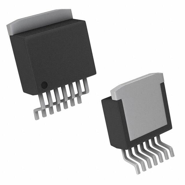
Packages:
– 7-lead TO-220, zip and straight leads
– 7-lead DDPAK surface-mount
2 Applications
•
•
•
•
•
•
Semiconductor manufacturing
Semiconductor test
Lab and field instrumentation
LCD test
Analog input module
Ultrasound scanner
Simplified Schematic
V+
VIN±
The OPA548 is internally protected against
overtemperature conditions and current overloads. In
addition, the OPA548 is designed to provide an
accurate, user-selected current limit. Unlike other
designs that use a power resistor in series with the
output current path, the OPA548 senses the load
indirectly. The current limit is adjustable from 0 A to 5
A with an external resistor and potentiometer, or
controllable digitally with a voltage-out or current-out
DAC.
The Enable/Status (E/S) pin provides two functions.
An input on the pin not only disables the output stage
to effectively disconnect the load, but also reduces
the quiescent current to conserve power. The E/S pin
output can be monitored to determine if the OPA548
is in thermal shutdown.
The OPA548 device is available in an industrystandard 7-lead staggered and straight lead TO-220
package, and a 7-lead DDPAK surface-mount plastic
power package. The copper tab allows easy
mounting to a heat sink or circuit board for excellent
thermal performance. The device is specified for
operation over the extended industrial temperature
range, –40°C to 85°C. A SPICE macromodel is
available for design analysis.
±
ILIM
+
RCL (¼W Resistor)
E/S
V±
Device Information(1)
VO
OPA548
VIN+
The OPA548 operates from either single or dual
supplies for design flexibility. In single-supply
operation, the input common-mode range extends
below ground.
RCL sets the current limit
value from 0 A to 5 A.
PART NUMBER
OPA548
PACKAGE
BODY SIZE (NOM)
TO-220 (7)
10.17 mm × 8.38 mm
TO-263 (7)
10.10 mm × 8.89 mm
(1) For all available packages, see the package option addendum
at the end of the data sheet.
1
An IMPORTANT NOTICE at the end of this data sheet addresses availability, warranty, changes, use in safety-critical applications,
intellectual property matters and other important disclaimers. PRODUCTION DATA.
�OPA548
SBOS070D – OCTOBER 1997 – REVISED DECEMBER 2019
www.ti.com
Table of Contents
1
2
3
4
5
6
7
Features ..................................................................
Applications ...........................................................
Description .............................................................
Revision History.....................................................
Pin Configuration and Functions .........................
Specifications.........................................................
1
1
1
2
3
4
6.1
6.2
6.3
6.4
6.5
6.6
4
4
4
4
5
7
Detailed Description ............................................ 11
7.1
7.2
7.3
7.4
8
Absolute Maximum Ratings ......................................
ESD Ratings..............................................................
Recommended Operating Conditions.......................
Thermal Information .................................................
Electrical Characteristics...........................................
Typical Characteristics ..............................................
Overview .................................................................
Functional Block Diagram .......................................
Feature Description.................................................
Device Functional Modes........................................
11
11
11
12
Application and Implementation ........................ 13
8.1 Application Information............................................ 13
8.2 Typical Applications ................................................ 13
8.3 System Examples ................................................... 20
9
Power Supply Recommendations...................... 22
9.1 Output Stage Compensation................................... 22
9.2 Output Protection .................................................... 22
10 Layout................................................................... 24
10.1 Layout Guidelines ................................................. 24
10.2 Layout Example .................................................... 28
11 Device and Documentation Support ................. 29
11.1
11.2
11.3
11.4
11.5
11.6
11.7
Device Support......................................................
Documentation Support ........................................
Receiving Notification of Documentation Updates
Support Resources ...............................................
Trademarks ...........................................................
Electrostatic Discharge Caution ............................
Glossary ................................................................
29
29
29
29
29
29
29
12 Mechanical, Packaging, and Orderable
Information ........................................................... 30
4 Revision History
NOTE: Page numbers for previous revisions may differ from page numbers in the current version.
Changes from Revision C (June 2015) to Revision D
Page
•
Changed all INPUT BIAS CURRENT specifications in MIN column to TYP column, and all specifications in TYP
column to MAX column (typo) ................................................................................................................................................ 5
•
Changed Quiescent current, shutdown mode parameter unit typo from nA to mA in Electrical Characteristics table .......... 6
•
Deleted Temperature Range section of Electrical Characteristics table; content already available in other
specifications tables................................................................................................................................................................ 6
•
Changed Figure 20 x-axis label from 2 µs/div to 5 µs/div, and y-axis label from 50 mV/div to 10 V/div ............................. 10
Changes from Revision B (October 2003) to Revision C
•
2
Page
Added ESD Ratings table, Feature Description section, Device Functional Modes, Application and Implementation
section, Power Supply Recommendations section, Layout section, Device and Documentation Support section, and
Mechanical, Packaging, and Orderable Information section ................................................................................................. 1
Submit Documentation Feedback
Copyright © 1997–2019, Texas Instruments Incorporated
Product Folder Links: OPA548
�OPA548
www.ti.com
SBOS070D – OCTOBER 1997 – REVISED DECEMBER 2019
5 Pin Configuration and Functions
KVT and KC Packages Stagger-Formed
7-Pin TO-220
Top View
KVT and KC Packages Straight-Formed
7-Pin TO-220
Top View
KTW Package Surface-Mount
7-Pin TO-263
Top View
Pin Functions
PIN
NO.
NAME
I/O
DESCRIPTION
1
VIN+
I
Noninverting input
2
VIN–
I
Inverting input
3
ILIM
I
Current limit set
4
V–
I
Negative power supply
5
V+
I
Positive power supply
6
VO
O
Output
7
E/S
I/O
Enable or disable control input, thermal shutdown status output
Submit Documentation Feedback
Copyright © 1997–2019, Texas Instruments Incorporated
Product Folder Links: OPA548
3
�OPA548
SBOS070D – OCTOBER 1997 – REVISED DECEMBER 2019
www.ti.com
6 Specifications
6.1 Absolute Maximum Ratings
over operating free-air temperature range (unless otherwise noted)
(1)
MIN
Output current
MAX
Supply voltage, V+ to V–
60
Input voltage
(V–) – 0.5V
(V+) + 0.5
Input shutdown voltage
–40
Junction temperature
(1)
V
V
V+
Operating temperature
Tstg
UNIT
See Figure 40
Storage temperature
–55
125
°C
150
°C
125
°C
Stresses beyond those listed under Absolute Maximum Ratings may cause permanent damage to the device. These are stress ratings
only, which do not imply functional operation of the device at these or any other conditions beyond those indicated under Recommended
Operating Conditions. Exposure to absolute-maximum-rated conditions for extended periods may affect device reliability.
6.2 ESD Ratings
VALUE
V(ESD)
(1)
Electrostatic discharge
Human-body model (HBM), per ANSI/ESDA/JEDEC JS-001 (1)
±2000
Machine model
±200
UNIT
V
JEDEC document JEP155 states that 500-V HBM allows safe manufacturing with a standard ESD control process.
6.3 Recommended Operating Conditions
over operating free-air temperature range (unless otherwise noted)
MIN
Supply voltage (V+ – V–)
Specified temperature
NOM
MAX
UNIT
8 (±4)
60 (±30)
V
–40
125
°C
6.4 Thermal Information
OPA548
THERMAL METRIC (1)
KVT and KC (TO-220)
KTW (DDPAK)
UNIT
7 PINS
7 PINS
RθJA
Junction-to-ambient thermal resistance
30.2
30.2
°C/W
RθJC(top)
Junction-to-case (top) thermal resistance
37.4
37.4
°C/W
RθJB
Junction-to-board thermal resistance
14.4
14.4
°C/W
ψJT
Junction-to-top characterization parameter
5.1
5.1
°C/W
ψJB
Junction-to-board characterization parameter
14.3
14.3
°C/W
RθJC(bot)
Junction-to-case (bottom) thermal resistance
0.2
0.2
°C/W
(1)
4
For more information about traditional and new thermal metrics, see the Semiconductor and IC Package Thermal Metrics application
report.
Submit Documentation Feedback
Copyright © 1997–2019, Texas Instruments Incorporated
Product Folder Links: OPA548
�OPA548
www.ti.com
SBOS070D – OCTOBER 1997 – REVISED DECEMBER 2019
6.5 Electrical Characteristics
over operating free-air temperature range (unless otherwise noted)
PARAMETER
TEST CONDITIONS
MIN
TYP
MAX
UNIT
±2
±10
mV
OFFSET VOLTAGE
Input offset voltage
VCM = 0 V, IO = 0 A
Input offset voltage drift
VCM = 0 V, IO = 0 A,
TA = –40°C to +85°C
±30
Power-supply rejection ratio
VCM = 0 V, IO = 0 A,
VS = ±4 V to ±30 V
30
100
–500
INPUT BIAS CURRENT
µV/°C
µV/V
(1)
Input bias current (2)
VCM = 0 V
–100
Input bias current drift
VCM = 0 V, TA = –40°C to +85°C
±0.5
Input offset current
VCM = 0 V
±5
nA
nA/°C
±50
nA
NOISE
Input voltage noise density
f = 1 kHz
90
nV/√Hz
Current noise density
f = 1 kHz
200
fA/√Hz
INPUT VOLTAGE
Common-mode voltage
Positive
Linear operation
(V+) – 3
(V+) – 2.3
Negative
Linear operation
(V–) – 0.1
(V–) – 0.2
80
95
Common-mode rejection
VCM = (V–) – 0.1 V to (V+) – 3 V
V
dB
INPUT IMPEDANCE
Differential input impedance
107 || 6
Ω || pF
Common-mode input impedance
109 || 4
Ω || pF
OPEN-LOOP GAIN
VO = ±25 V, RL = 1 kΩ
Open-loop voltage gain
90
VO = ±25 V, RL = 8 Ω
98
dB
90
dB
1
MHz
10
V/µs
FREQUENCY RESPONSE
Gain-bandwidth product
RL = 8 Ω
Slew rate
G = 1, VO = 50 VPP, RL = 8 Ω
Full-power bandwidth
See Typical Characteristics
Settling time
To ±0.1%, G = –10, VO = 50 VPP
Total harmonic distortion + noise
(3)
kHz
15
f = 1 kHz, RL = 8 Ω, G = 3,
Power = 10 W
µs
0.02%
OUTPUT
Voltage output
Maximum continuous
current output
Positive
IO = 3 A
(V+) – 4.1
(V+) – 3.7
Negative
IO = –3 A
(V–) + 3.7
(V–) + 3.3
Positive
IO = 0.6 A
(V+) – 2.4
(V+) – 2.1
Negative
IO = –0.6 A
(V–) + 1.3
(V–) + 1.0
DC
±3
A
AC
3
Arms
Leakage current, output disabled, dc
See Typical Characteristics
Output current limit
–5
Output current limit tolerance (1)
5
A
ILIM = (15000)(4.75) / (13750 Ω +
RCL)
Output current limit equation
RCL = 14.8 kΩ (ILIM = ±2.5 A),
RL = 8 Ω
Capacitive load drive
(1)
(2)
(3)
V
±100
±250
A
mA
See Figure 19
High-speed test at TJ = 25°C.
Positive conventional current flows into the input terminals.
See Figure 12 for additional power levels.
Submit Documentation Feedback
Copyright © 1997–2019, Texas Instruments Incorporated
Product Folder Links: OPA548
5
�OPA548
SBOS070D – OCTOBER 1997 – REVISED DECEMBER 2019
www.ti.com
Electrical Characteristics (continued)
over operating free-air temperature range (unless otherwise noted)
PARAMETER
TEST CONDITIONS
MIN
TYP
VE/S HIGH (output enabled)
E/S pin open or forced high
(V–) + 2.4
VE/S LOW (output disabled)
E/S pin forced low
IE/S HIGH (output enabled)
E/S pin high
–65
IE/S LOW (output disabled)
E/S pin low
–70
MAX
UNIT
OUTPUT ENABLE /STATUS (E/S) PIN
Shutdown
input
mode
(V–) + 0.8
V
µA
Output disable time
1
µs
Output enable time
3
µs
Normal operation, sourcing 20 µA
Thermal shutdown status output
Thermally shut down,
sinking 5 µA, TJ > 160°C
(V–) + 2.4
(V–) + 3.5
(V–) +
0.35
Shutdown
160
Reset from shutdown
140
Quiescent current
ILIM connected to V–, IO = 0 A
±17
Quiescent current, shutdown mode
ILIM connected to V–, IO = 0 A
±6
Thermal protection junction temperature
(V–) + 0.8
V
°C
POWER SUPPLY
6
Submit Documentation Feedback
±20
mA
mA
Copyright © 1997–2019, Texas Instruments Incorporated
Product Folder Links: OPA548
�OPA548
www.ti.com
SBOS070D – OCTOBER 1997 – REVISED DECEMBER 2019
6.6 Typical Characteristics
at TCASE = 25°C, VS = ±30V, and E/S pin open (unless otherwise noted)
Figure 1. Open-Loop Gain and Phase vs Frequency
Figure 2. Input Bias Current vs Temperature
Figure 3. Current Limit vs Temperature
Figure 4. Current Limit vs Supply Voltage
Figure 5. Input Bias Current vs Common-Mode Voltage
Figure 6. Quiescent Current vs Temperature
Submit Documentation Feedback
Copyright © 1997–2019, Texas Instruments Incorporated
Product Folder Links: OPA548
7
�OPA548
SBOS070D – OCTOBER 1997 – REVISED DECEMBER 2019
www.ti.com
Typical Characteristics (continued)
at TCASE = 25°C, VS = ±30V, and E/S pin open (unless otherwise noted)
8
Figure 7. Common-Mode Rejection vs Frequency
Figure 8. Power-Supply Rejection vs Frequency
Figure 9. Voltage Noise Density vs Frequency
Figure 10. Open-loop Gain, Common-Mode Rejection,
and Power-Supply Rejection vs Temperature
Figure 11. Gain-Bandwidth Product and Slew Rate vs
Temperature
Figure 12. Total Harmonic Distortion+Noise vs Frequency
Submit Documentation Feedback
Copyright © 1997–2019, Texas Instruments Incorporated
Product Folder Links: OPA548
�OPA548
www.ti.com
SBOS070D – OCTOBER 1997 – REVISED DECEMBER 2019
Typical Characteristics (continued)
5
5
4
4
| VSUPPLY | – | VOUT | (V)
| VSUPPLY | – | VOUT | (V)
at TCASE = 25°C, VS = ±30V, and E/S pin open (unless otherwise noted)
(V+) – VO
3
|(V–) – VO|
2
1
IO = +3 A
IO = –3 A
3
2
IO = +0.6 A
1
IO = –0.6 A
0
0
0
1
2
3
4
–75
–50
–25
0
25
50
75
100
125
Output Current (A)
Temperature (°C)
Figure 13. Output Voltage Swing vs Output Current
Figure 14. Output Voltage Swing vs Temperature
Figure 15. Maximum Output Voltage Swing vs Frequency
Figure 16. Output Leakage Current vs Applied Output
Voltage
Figure 17. Offset Voltage Production Distribution
Figure 18. Offset Voltage Drift Production Distribution
Submit Documentation Feedback
Copyright © 1997–2019, Texas Instruments Incorporated
Product Folder Links: OPA548
9
�OPA548
SBOS070D – OCTOBER 1997 – REVISED DECEMBER 2019
www.ti.com
Typical Characteristics (continued)
10 V/div
at TCASE = 25°C, VS = ±30V, and E/S pin open (unless otherwise noted)
5 µs/div
G=3
Figure 19. Small-Signal Overshoot vs Load Capacitance
G=1
CL = 1000 pF
Submit Documentation Feedback
RL = 8 Ω
Figure 20. Large-Signal Step Response
G=3
Figure 21. Small-Signal Step Response
10
CL = 1000 pF,
CL = 1000 pF
Figure 22. Small-Signal Step Response
Copyright © 1997–2019, Texas Instruments Incorporated
Product Folder Links: OPA548
�OPA548
www.ti.com
SBOS070D – OCTOBER 1997 – REVISED DECEMBER 2019
7 Detailed Description
7.1 Overview
The OPA548 device uses a PNP input stage (resulting in negative bias currents at each input) without input bias
current compensation so matched resistances on the inputs will reduce errors. After the main voltage gain stage
is the high current output stage with temperature compensated class A/B biasing to reduce crossover distortion.
Local feedback in the output stage may require additional compensation for highly reactive loads (see Output
Stage Compensation).
7.2 Functional Block Diagram
V+
V-IN
Differential
Amplifier
V+IN
High Current
Output Stage
Voltage
Amplifier
Biasing
Current Limiting
Enable/Disable
Alarms
VO
ILIM
V-
E/S
7.3 Feature Description
7.3.1 Adjustable Current Limit
The OPA548 features an accurate, user-selected current limit. The current limit is set from 0 A to 5 A by
controlling the input to the ILIM pin. Unlike other designs, which use a power resistor in series with the output
current path, the OPA548 senses the load indirectly. This allows the current limit to be set with a 0-μA to 330-μA
control signal. In contrast, other designs require a limiting resistor to handle the full output current (5 A in this
case).
With the OPA548, the simplest method for adjusting the current limit uses a resistor or potentiometer connected
between the ILIM pin and V– according to the Equation 1:
(15000)(4.75)
RCL =
- 13750 W
ILIM
(1)
The low-level control signal (0 μA to 330 μA) also allows the current limit to be digitally controlled.
See Figure 41 for a simplified schematic of the internal circuitry used to set the current limit. Leaving the ILIM pin
open programs the output current to zero, while connecting ILIM directly to V– programs the maximum output
current limit, typically 5 A.
Submit Documentation Feedback
Copyright © 1997–2019, Texas Instruments Incorporated
Product Folder Links: OPA548
11
�OPA548
SBOS070D – OCTOBER 1997 – REVISED DECEMBER 2019
www.ti.com
Feature Description (continued)
7.3.2 Enable/Status (E/S) Pin
The Enable/Status pin provides two functions: forcing this pin LOW disables the output stage, or E/S can be
monitored to determine if the OPA548 is in thermal shutdown. One or both of these functions can be used on the
same device using single or dual supplies. For normal operation (output enabled), the E/S pin can be left open or
pulled HIGH (at least 2.4 V more than the negative rail). A small value capacitor connected between the E/S pin
and V– may be required for noisy applications.
7.3.3 Thermal Shutdown Status
Internal thermal shutdown circuitry shuts down the output when the die temperature reaches approximately
160°C, resetting when the die has cooled to 140°C. The E/S pin can be monitored to determine if shutdown has
occurred. During normal operation the voltage on the E/S pin is typically 3.5 V more than the negative rail. Once
shutdown has occurred, this voltage drops to approximately 350 mV more than the negative rail.
7.4 Device Functional Modes
7.4.1 Output Disable
A unique feature of the OPA548 is its output disable capability. This function not only conserves power during
idle periods (quiescent current drops to approximately 6 mA), but also allows multiplexing in low frequency (f <
20 kHz), multichannel applications. Signals greater than 20 kHz may cause leakage current to increase in
devices that are shutdown. Figure 33 shows the two OPA548s in a switched amplifier configuration. The ON/OFF
state of the two amplifiers is controlled by the voltage on the E/S pin.
To disable the output, the E/S pin is pulled LOW, no greater than 0.8 V more than the negative rail. Typically the
output is shutdown in 1 μs. Figure 23 provides an example of how to implement this function using a single
supply. Figure 24 gives a circuit for dual-supply applications. To return the output to an enabled state, the E/S pin
should be disconnected (open) or pulled to at least (V–) + 2.4 V. It should be noted that pulling the E/S pin HIGH
(output enabled) does not disable internal thermal shutdown.
Figure 23. Output Disable With a Single Supply
12
Figure 24. Output Disable With Dual Supplies
Submit Documentation Feedback
Copyright © 1997–2019, Texas Instruments Incorporated
Product Folder Links: OPA548
�OPA548
www.ti.com
SBOS070D – OCTOBER 1997 – REVISED DECEMBER 2019
8 Application and Implementation
NOTE
Information in the following applications sections is not part of the TI component
specification, and TI does not warrant its accuracy or completeness. TI’s customers are
responsible for determining suitability of components for their purposes. Customers should
validate and test their design implementation to confirm system functionality.
8.1 Application Information
The OPA548 is specified for operation from 8 V to 60 V (±4 V to ±30 V). Specifications apply over the –40°C to
85°C temperature range while the device operates from –40°C to 125°C. Parameters that can exhibit significant
variance with regard to operating voltage or temperature are presented in Typical Characteristics.
8.2 Typical Applications
8.2.1 Basic Circuit Connections
Figure 25 shows the OPA548 connected as a basic noninverting amplifier. The OPA548 can be used in virtually
any operational amplifier configuration.
Power-supply terminals should be bypassed with low series impedance capacitors. The technique shown in
Figure 44, using a ceramic and tantalum type in parallel is recommended. In addition, we recommend a 0.01-μF
capacitor between V+ and V– as close to the OPA548 as possible. Power-supply wiring should have low series
impedance.
Figure 25. Basic Circuit Connections Example
Submit Documentation Feedback
Copyright © 1997–2019, Texas Instruments Incorporated
Product Folder Links: OPA548
13
�OPA548
SBOS070D – OCTOBER 1997 – REVISED DECEMBER 2019
www.ti.com
Typical Applications (continued)
8.2.1.1 Design Requirements
To
•
•
•
•
•
design an example of a noninverting circuit, the following requirements are spelled out:
Gain: 1
Output voltage swing: ±10 V
Maximum Output Current: ±2.5 A
Load: 4-Ω resistive
Ambient Temperature: Up to 40°C
Figure 26. Noninverting Amplifier Configuration Schematic
8.2.1.2 Detailed Design Procedure
8.2.1.2.1 Power Supply Requirements
Select the power supply based on the requirement to achieve a ±10-V output with up to a 2.5-A load. The
maximum value for output voltage swing at 3-A is approximately within 4 V of either rail, standard 15-V power
supplies rated at >2.5 A each will suffice.
8.2.1.2.2 Gain Setting and Input Configuration
A unity gain noninverting application could be provided by simply connecting the output of an operational
amplifier back to its input, with the signal applied to the noninverting input. Power operational amplifiers are
frequently subject to unpredictable load impedances that can cause instability. Increasing gain can enhance
stability. Furthermore, the feedback network provides locations for further opportunities for stability enhancing
components if necessary.
In this application two 10-kΩ resistors are used for the input and feedback resistance, which would normally
result in a noninverting gain of 2. Adding a voltage divider consisting of R1 and R2 reduces the input signal by
half before it is applied to the operational amplifier. In this case the solution just happens to restore us back to
the desired overall gain of 1. This solution using an identical pair of resistors before the noninverting input
between the signal and ground creates what is known as a difference amplifier.
14
Submit Documentation Feedback
Copyright © 1997–2019, Texas Instruments Incorporated
Product Folder Links: OPA548
�OPA548
www.ti.com
SBOS070D – OCTOBER 1997 – REVISED DECEMBER 2019
Typical Applications (continued)
8.2.1.2.3 Current Limit
The OPA548 provides means to limit the maximum output current delivered by the amplifier. A resistor between
the negative supply and the amplifier`s Ilim pin, or a DAC can be used to set the current limit. For this circuit a
14.7-kΩ resistor (Rcl) limits the output current to approximately 2.5 A.
8.2.1.2.4 Safe-Operating-Area
Plotting the load on the Safe-Operating-Area (SOA) curve allows the safety of the application to be assessed.
Figure 40 depicts the 4-Ω load on the curve. With a resistive load, maximum dissipation occurs at an output
voltage one-half of the supply voltage, in this case 7.5 V and 1.875 A for 22.5 W.
Consideration should be given to the condition of a shorted output. In this application this is a stress of 15 V at
2.5 A on the output stage, or 37.5 W which is just within the 50-W SOA of the OPA548. How long the circuit can
withstand a short to ground will be determined by the size of the heatsink. Ultimately the thermal shutdown will
activate providing short circuit protection, although even this is not recommended as a continuous condition.
8.2.1.2.5 Heat Sinking
From Safe-Operating-Area we know we will must support 22.5 W of dissipation up to the 40°C ambient
requirements of the application. This indicates the need for a heatsink with a RθHA < 2.5°C/W, such as an Aavid
Thermalloy 530002B02500G.
8.2.1.3 Application Curve
Figure 27 shows the expected results for the Noninverting Operation of the OPA548. The left picture shows the
Noninverting Operation in dual supply mode and the right picture shows the Noninverting Operation in single
supply mode. The input signal is a zero-centered sine wave with an amplitude of 10 V p-p and a frequency of 1
kHz. In this trace the OPA548 is delivering a peak current of 1.25 A to the 4-Ω load.
Figure 27. Noninverting Operation, Dual-Supply Waveforms
Submit Documentation Feedback
Copyright © 1997–2019, Texas Instruments Incorporated
Product Folder Links: OPA548
15
�OPA548
SBOS070D – OCTOBER 1997 – REVISED DECEMBER 2019
www.ti.com
Typical Applications (continued)
8.2.2 Monitoring Single- and Dual-Supplies
Figure 28 gives an example of monitoring shutdown in a single-supply application. Figure 29 provides a circuit for
dual supplies. External logic circuitry or an LED could be used to indicate if the output has been thermally
shutdown, see Figure 31.
Figure 28. Thermal Shutdown Status With a SingleSupply
Figure 29. Thermal Shutdown Status With DualSupplies
8.2.2.1 Design Requirements
See the previous Design Requirements.
8.2.2.2 Detailed Design Procedure
8.2.2.2.1 Output Disable and Thermal Shutdown Status
As mentioned earlier, the OPA548’s output can be disabled and the disable status can be monitored
simultaneously. Figure 28 and Figure 29 provide examples interfacing to the E/S pin while using a single supply
and dual supplies, respectively.
16
Submit Documentation Feedback
Copyright © 1997–2019, Texas Instruments Incorporated
Product Folder Links: OPA548
�OPA548
www.ti.com
SBOS070D – OCTOBER 1997 – REVISED DECEMBER 2019
Typical Applications (continued)
8.2.3 Programmable Power Supply
A programmable source or sink power supply can easily be built using the OPA548. Both the output voltage and
output current are user-controlled. See Figure 30 for a circuit using potentiometers to adjust the output voltage
and current while Figure 31 uses DACs. An LED tied to the E/S pin through a logic gate indicates if the OPA548
is in thermal shutdown.
Figure 30 illustrates how to use the OPA548 to provide an accurate voltage source with only three external
resistors. First, the current limit resistor, RCL, is chosen according to the desired output current. The resulting
voltage at the ILIM pin is constant and stable over temperature. This voltage, VCL, is connected to the noninverting
input of the operational amplifier and used as a voltage reference, thus eliminating the need for an external
reference. The feedback resistors are selected to gain VCL to the desired output voltage level.
Figure 30. Voltage Source Schematic
Submit Documentation Feedback
Copyright © 1997–2019, Texas Instruments Incorporated
Product Folder Links: OPA548
17
�OPA548
SBOS070D – OCTOBER 1997 – REVISED DECEMBER 2019
www.ti.com
Typical Applications (continued)
Figure 31. Resistor-Controlled Programmable Power Supply Schematic
18
Submit Documentation Feedback
Copyright © 1997–2019, Texas Instruments Incorporated
Product Folder Links: OPA548
�OPA548
www.ti.com
SBOS070D – OCTOBER 1997 – REVISED DECEMBER 2019
Typical Applications (continued)
Figure 32. Digitally-Controlled Programmable Power Supply Schematic
Submit Documentation Feedback
Copyright © 1997–2019, Texas Instruments Incorporated
Product Folder Links: OPA548
19
�OPA548
SBOS070D – OCTOBER 1997 – REVISED DECEMBER 2019
www.ti.com
8.3 System Examples
Figure 33. Switched Amplifier Schematic
Figure 34. Multiple Current Limit Values Schematic
20
Submit Documentation Feedback
Copyright © 1997–2019, Texas Instruments Incorporated
Product Folder Links: OPA548
�OPA548
www.ti.com
SBOS070D – OCTOBER 1997 – REVISED DECEMBER 2019
System Examples (continued)
Figure 35. Single Quadrant V × I Limiting
Figure 36. Parallel Output for Increased Output Current Schematic
Submit Documentation Feedback
Copyright © 1997–2019, Texas Instruments Incorporated
Product Folder Links: OPA548
21
�OPA548
SBOS070D – OCTOBER 1997 – REVISED DECEMBER 2019
www.ti.com
9 Power Supply Recommendations
The OPA548 operates from single (8 V to 60 V) or dual (±4 V to ±30 V) supplies with excellent performance.
Most behavior remains unchanged throughout the full operating voltage range. Parameters which vary
significantly with operating voltage are shown Typical Characteristics.
Some applications do not require equal positive and negative output voltage swing. Power-supply voltages do
not must be equal. The OPA548 can operate with as little as 8 V between the supplies and with up to 60 V
between the supplies. For example, the positive supply could be set to 55 V with the negative supply at –5 V, or
vice-versa.
9.1 Output Stage Compensation
The complex load impedances common in power operational amplifier applications can cause output stage
instability. For normal operation output compensation circuitry is typically not required. However, if the OPA548 is
intended to be driven into current limit, an R/C network may be required. See Figure 38 for an output series R/C
compensation (snubber) network which generally provides excellent stability.
A snubber circuit may also enhance stability when driving large capacitive loads (> 1000 pF) or inductive loads
(motors, loads separated from the amplifier by long cables). Typically 3 Ω to 10 Ω in series with 0.01 μF to 0.1 μF
is adequate. Some variations in circuit value may be required with certain loads.
9.2 Output Protection
Reactive and EMF-generating loads can return load current to the amplifier, causing the output voltage to exceed
the power-supply voltage. This damaging condition can be avoided with clamp diodes from the output terminal to
the power supplies, as shown in Figure 38. Schottky rectifier diodes with a 5 A or greater continuous rating are
recommended.
Figure 37. Output Disable and Thermal Shutdown
Status With a Single Supply
22
Submit Documentation Feedback
Figure 38. Motor Drive Circuit
Copyright © 1997–2019, Texas Instruments Incorporated
Product Folder Links: OPA548
�OPA548
www.ti.com
SBOS070D – OCTOBER 1997 – REVISED DECEMBER 2019
Output Protection (continued)
Figure 39. Output Disable and Thermal Shutdown Status With Dual Supplies
Submit Documentation Feedback
Copyright © 1997–2019, Texas Instruments Incorporated
Product Folder Links: OPA548
23
�OPA548
SBOS070D – OCTOBER 1997 – REVISED DECEMBER 2019
www.ti.com
10 Layout
10.1 Layout Guidelines
10.1.1 Safe Operating Area
Stress on the output transistors is determined both by the output current and by the output voltage across the
conducting output transistor, VS – VO. The power dissipated by the output transistor is equal to the product of the
output current and the voltage across the conducting transistor, VS – VO. The Safe Operating Area (SOA curve,
Figure 40) shows the permissible range of voltage and current.
Figure 40. 4-Ω Load Plotted on OPA548 SOA for this Application
The safe output current decreases as VS – VO increases. Output short circuits are a very demanding case for
SOA. A short-circuit to ground forces the full power-supply voltage (V+ or V–) across the conducting transistor.
Increasing the case temperature reduces the safe output current that can be tolerated without activating the
thermal shutdown circuit of the OPA548. For further insight on SOA, consult Application Bulletin SBOA022.
24
Submit Documentation Feedback
Copyright © 1997–2019, Texas Instruments Incorporated
Product Folder Links: OPA548
�OPA548
www.ti.com
SBOS070D – OCTOBER 1997 – REVISED DECEMBER 2019
Layout Guidelines (continued)
10.1.2 Amplifier Mounting
Figure 46 provides recommended solder footprints for both the TO-220 and DDPAK power packages. The tab of
both packages is electrically connected to the negative supply, V–. It may be desirable to isolate the tab of the
TO-220 package from its mounting surface with a mica (or other film) insulator (see Figure 42). For lowest overall
thermal resistance it is best to isolate the entire heat sink/OPA548 structure from the mounting surface rather
than to use an insulator between the semiconductor and heat sink.
For best thermal performance, the tab of the DDPAK surface-mount version should be soldered directly to a
circuit board copper area. Increasing the copper area improves heat dissipation. See Figure 43 for typical
thermal resistance from junction-to-ambient as a function of the copper area.
Figure 41. Adjustable Current Limit
Submit Documentation Feedback
Copyright © 1997–2019, Texas Instruments Incorporated
Product Folder Links: OPA548
25
�OPA548
SBOS070D – OCTOBER 1997 – REVISED DECEMBER 2019
www.ti.com
Layout Guidelines (continued)
10.1.3 Power Dissipation
Power dissipation depends on power supply, signal, and load conditions. For DC signals, power dissipation is
equal to the product of output current times the voltage across the conducting output transistor. Power
dissipation can be minimized by using the lowest possible power-supply voltage necessary to assure the
required output voltage swing.
For resistive loads, the maximum power dissipation occurs at a DC output voltage of one-half the power-supply
voltage. Dissipation with AC signals is lower. Application Bulletin SBOA022 explains how to calculate or measure
power dissipation with unusual signals and loads.
Figure 42. TO-220 Thermal Resistance vs Aluminum Plate Area
Figure 43. DDPAK Thermal Resistance vs Circuit Board Copper Area
10.1.4 Thermal Considerations
Power dissipated in the OPA548 will cause the junction temperature to rise. The OPA548 has thermal shutdown
circuitry that protects the amplifier from damage. The thermal protection circuitry disables the output when the
junction temperature reaches approximately 160°C, allowing the device to cool. When the junction temperature
cools to approximately 140°C, the output circuitry is again enabled. Depending on load and signal conditions, the
thermal protection circuit may cycle on and off. This limits the dissipation of the amplifier but may have an
undesirable effect on the load.
26
Submit Documentation Feedback
Copyright © 1997–2019, Texas Instruments Incorporated
Product Folder Links: OPA548
�OPA548
www.ti.com
SBOS070D – OCTOBER 1997 – REVISED DECEMBER 2019
Layout Guidelines (continued)
Any tendency to activate the thermal protection circuit indicates excessive power dissipation or an inadequate
heat sink. For reliable operation, junction temperature should be limited to 125°C, maximum. To estimate the
margin of safety in a complete design (including heat sink) increase the ambient temperature until the thermal
protection is triggered. Use worst-case load and signal conditions. For good reliability, thermal protection should
trigger more than 35°C more than the maximum expected ambient condition of your application. This produces a
junction temperature of 125°C at the maximum expected ambient condition.
The internal protection circuitry of the OPA548 was designed to protect against overload conditions. It was not
intended to replace proper heat sinking. Continuously running the OPA548 into thermal shutdown will degrade
reliability.
10.1.5 Heat Sinking
Most applications require a heat sink to assure that the maximum operating junction temperature (125°C) is not
exceeded. In addition, the junction temperature should be kept as low as possible for increased reliability.
Junction temperature can be determined according to the equation:
TJ = TA + PDRθJA
where
•
•
•
•
•
•
•
•
RθJA = RθJC + RθCH + RθHA
TJ = Junction Temperature (°C)
TA = Ambient Temperature (°C)
PD = Power Dissipated (W)
RθJC = Junction-to-Case Thermal Resistance (°C/W)
RθCH = Case-to-Heat Sink Thermal Resistance (°C/W)
RθHA = Heat Sink-to-Ambient Thermal Resistance (°C/W)
RθJA = Junction-to-Air Thermal Resistance (°C/W)
(2)
Figure 44 shows maximum power dissipation versus ambient temperature with and without the use of a heat
sink. Using a heat sink significantly increases the maximum power dissipation at a given ambient temperature as
shown.
Power Dissipation (W)
The difficulty in selecting the heat sink required lies in determining the power dissipated by the OPA548. For DC
output into a purely resistive load, power dissipation is simply the load current times the voltage developed
across the conducting output transistor, PD = IL(VS–VO). Other loads are not as simple. Consult Application
Bulletin SBOA022 for further insight on calculating power dissipation. Once power dissipation for an application is
known, the proper heat sink can be selected.
TO-220 with Thermalloy
6030B Heat Sink
RθJA= 16.7°C/W
PD = (TJ(max) – TA) / RθJA
TJ(max) = 150°C
With infinite heat sink
(RθJA = 2.5°C/W),
max PD = 50 W at TA = 25°C
DDPAK
RθJA= 26°C/W
2
(3 in , 1-oz. copper
mounting pad)
DDPAK or TO-220
RθJA= 65°C/W (no heat sink)
Ambient Temperature (°C)
Figure 44. Maximum Power Dissipation vs Ambient Temperature
Submit Documentation Feedback
Copyright © 1997–2019, Texas Instruments Incorporated
Product Folder Links: OPA548
27
�OPA548
SBOS070D – OCTOBER 1997 – REVISED DECEMBER 2019
www.ti.com
Layout Guidelines (continued)
10.1.5.1 Heat Sink Selection Example
A TO-220 package is dissipating 5 W. The maximum expected ambient temperature is 40°C. Find the proper
heat sink to keep the junction temperature less than 125°C (150°C minus 25°C safety margin).
Combining Equation 2 and Equation 3 gives:
TJ = TA + PD(RθJC + RθCH + RθHA)
(3)
TJ, TA, and PD are given. RθJC is provided in the specification table, 2.5°C/W (DC). RθCH can be obtained from the
heat sink manufacturer. Its value depends on heat sink size, area, and material used. Semiconductor package
type, mounting screw torque, insulating material used (if any), and thermal joint compound used (if any) also
affect RθCH. A typical RθCH for a TO-220 mounted package is 1°C/W. Now we can solve for RθHA:
T - TA
qHA = J
- (qJC + qCH )
PD
qHA =
125°C - 40°C
- (2.5°C / W + 1°C / W ) = 13.5°C / W
5W
(4)
To maintain junction temperature less than 125°C, the heat sink selected must have a RθHA less than 14°C/W. In
other words, the heat sink temperature rise above ambient must be less than 67.5°C (13.5°C/W × 5 W). For
example, at 5-W Thermalloy model number 6030B has a heat sink temperature rise of 66°C more than ambient
(RθHA = 66°C / 5 W = 13.2°C / W), which is less than the 67.5°C required in this example. Figure 44 shows power
dissipation versus ambient temperature for a TO-220 package with a 6030B heat sink.
Another variable to consider is natural convection versus forced convection air flow. Forced-air cooling by a small
fan can lower RθJCA (RθCH + RθHA) dramatically. Heat sink manufactures provide thermal data for both of these
cases. For additional information on determining heat sink requirements, consult Application Bulletin SBOA021.
As mentioned earlier, once a heat sink has been selected, the complete design should be tested under worstcase load and signal conditions to maintain proper thermal protection.
10.2 Layout Example
V- V+
0.01µF
bypass
Grey area is
ground layer
0.1µF
bypasses
RILIM
Output
E/S
R1
R2
VIN
Figure 45. Recommended Layout Example
28
Submit Documentation Feedback
Copyright © 1997–2019, Texas Instruments Incorporated
Product Folder Links: OPA548
�OPA548
www.ti.com
SBOS070D – OCTOBER 1997 – REVISED DECEMBER 2019
11 Device and Documentation Support
11.1 Device Support
11.1.1 Third-Party Products Disclaimer
TI'S PUBLICATION OF INFORMATION REGARDING THIRD-PARTY PRODUCTS OR SERVICES DOES NOT
CONSTITUTE AN ENDORSEMENT REGARDING THE SUITABILITY OF SUCH PRODUCTS OR SERVICES
OR A WARRANTY, REPRESENTATION OR ENDORSEMENT OF SUCH PRODUCTS OR SERVICES, EITHER
ALONE OR IN COMBINATION WITH ANY TI PRODUCT OR SERVICE.
11.2 Documentation Support
11.2.1 Related Documentation
Texas Instruments, Heat Sinking — TO-3 Thermal ModelSBOA021 applicaiton bulletin
11.3 Receiving Notification of Documentation Updates
To receive notification of documentation updates, navigate to the device product folder on ti.com. In the upper
right corner, click on Alert me to register and receive a weekly digest of any product information that has
changed. For change details, review the revision history included in any revised document.
11.4 Support Resources
TI E2E™ support forums are an engineer's go-to source for fast, verified answers and design help — straight
from the experts. Search existing answers or ask your own question to get the quick design help you need.
Linked content is provided "AS IS" by the respective contributors. They do not constitute TI specifications and do
not necessarily reflect TI's views; see TI's Terms of Use.
11.5 Trademarks
E2E is a trademark of Texas Instruments.
All other trademarks are the property of their respective owners.
11.6 Electrostatic Discharge Caution
These devices have limited built-in ESD protection. The leads should be shorted together or the device placed in conductive foam
during storage or handling to prevent electrostatic damage to the MOS gates.
11.7 Glossary
SLYZ022 — TI Glossary.
This glossary lists and explains terms, acronyms, and definitions.
Submit Documentation Feedback
Copyright © 1997–2019, Texas Instruments Incorporated
Product Folder Links: OPA548
29
�OPA548
SBOS070D – OCTOBER 1997 – REVISED DECEMBER 2019
www.ti.com
12 Mechanical, Packaging, and Orderable Information
The following pages include mechanical, packaging, and orderable information. This information is the most
current data available for the designated devices. This data is subject to change without notice and revision of
this document. For browser-based versions of this data sheet, refer to the left-hand navigation.
(1)
For improved thermal performance, increase footprint area. See Figure 43.
(2)
Mean dimensions in inches. Refer to the mechanical drawings or www.ti.com for tolerances and detailed package
drawings.
Figure 46. TO-220 and DDPAK Solder Footprints
30
Submit Documentation Feedback
Copyright © 1997–2019, Texas Instruments Incorporated
Product Folder Links: OPA548
�PACKAGE OPTION ADDENDUM
www.ti.com
13-Aug-2021
PACKAGING INFORMATION
Orderable Device
Status
(1)
Package Type Package Pins Package
Drawing
Qty
Eco Plan
(2)
Lead finish/
Ball material
MSL Peak Temp
Op Temp (°C)
Device Marking
(3)
(4/5)
(6)
OPA548F/500
ACTIVE
DDPAK/
TO-263
KTW
7
500
RoHS & Green
Call TI | SN
Level-2-260C-1 YEAR
-40 to 85
OPA548F
OPA548F/500G3
ACTIVE
DDPAK/
TO-263
KTW
7
500
RoHS & Green
SN
Level-2-260C-1 YEAR
-40 to 85
OPA548F
OPA548FKTWT
ACTIVE
DDPAK/
TO-263
KTW
7
250
RoHS & Green
Call TI | SN
Level-2-260C-1 YEAR
-40 to 85
OPA548F
OPA548FKTWTG3
ACTIVE
DDPAK/
TO-263
KTW
7
250
RoHS & Green
SN
Level-2-260C-1 YEAR
-40 to 85
OPA548F
OPA548T
ACTIVE
TO-220
KVT
7
50
RoHS & Green
Call TI | SN
N / A for Pkg Type
-40 to 85
OPA548T
OPA548T-1
ACTIVE
TO-220
KC
7
50
RoHS & Green
Call TI | SN
N / A for Pkg Type
-40 to 85
OPA548T
OPA548T-1G3
ACTIVE
TO-220
KC
7
50
RoHS & Green
SN
N / A for Pkg Type
-40 to 85
OPA548T
OPA548TG3
ACTIVE
TO-220
KVT
7
50
RoHS & Green
SN
N / A for Pkg Type
-40 to 85
OPA548T
(1)
The marketing status values are defined as follows:
ACTIVE: Product device recommended for new designs.
LIFEBUY: TI has announced that the device will be discontinued, and a lifetime-buy period is in effect.
NRND: Not recommended for new designs. Device is in production to support existing customers, but TI does not recommend using this part in a new design.
PREVIEW: Device has been announced but is not in production. Samples may or may not be available.
OBSOLETE: TI has discontinued the production of the device.
(2)
RoHS: TI defines "RoHS" to mean semiconductor products that are compliant with the current EU RoHS requirements for all 10 RoHS substances, including the requirement that RoHS substance
do not exceed 0.1% by weight in homogeneous materials. Where designed to be soldered at high temperatures, "RoHS" products are suitable for use in specified lead-free processes. TI may
reference these types of products as "Pb-Free".
RoHS Exempt: TI defines "RoHS Exempt" to mean products that contain lead but are compliant with EU RoHS pursuant to a specific EU RoHS exemption.
Green: TI defines "Green" to mean the content of Chlorine (Cl) and Bromine (Br) based flame retardants meet JS709B low halogen requirements of


 工商网监
湘ICP备2023018690号
工商网监
湘ICP备2023018690号
