Product
Folder
Order
Now
Support &
Community
Tools &
Software
Technical
Documents
OPA818
SBOS940A – MAY 2019 – REVISED MARCH 2020
OPA818 2.7-GHz, High-Voltage, FET-Input, Low Noise, Operational Amplifier
1 Features
3 Description
•
The OPA818 is a decompensated, voltage-feedback
operational amplifier for high-speed and wide
dynamic range applications. OPA818 has a low-noise
junction gate field-effect transistor (JFET) input stage
that combines high gain-bandwidth with a wide supply
range from 6 V to 13 V. The fast slew rate of
1400 V/µs provides high large-signal bandwidth and
low distortion. This amplifier is manufactured using
Texas Instruments' proprietary, high-speed, silicongermanium (SiGe) process to achieve significant
performance improvements over other high-speed,
FET-input amplifiers.
•
•
•
•
•
•
•
•
•
•
High speed:
– Gain-bandwidth product: 2.7 GHz
– Bandwidth (G = 7 V/V): 765 MHz
– Large-signal bandwidth (2 VPP): 400 MHz
– Slew rate: 1400 V/µs
Decompensated gain: 7-V/V stable
Low noise:
– Input voltage noise: 2.2 nV/√Hz
– Input current noise: 3 fA/√Hz (f = 10 kHz)
Input bias current: 4 pA (typical)
Low input capacitance:
– Common-mode: 1.9 pF
– Differential mode: 0.5 pF
Low distortion (G = 7 V/V, RL = 1 kΩ, VO = 2 VPP):
– HD2, HD3 at 1 MHz: –104 dBc, –108 dBc
– HD2, HD3 at 50 MHz: –57 dBc, –72 dBc
Wide supply range: 6 V to 13 V
Output swing: 8 VPP (VS = 10 V)
Supply current: 27.7 mA
Shutdown supply current: 27 µA
Performance upgrade to OPA657
2 Applications
•
•
•
•
•
•
•
•
The OPA818 is available in an 8-lead WSON
package with an exposed thermal pad for heat
dissipation. This device is specified to operate over
the industrial temperature range of –40°C to +85°C.
Wideband transimpedance amplifiers (TIAs)
Wafer scanning equipment
Optical communication modules
High-speed data acquisition (DAQ)
Active probes
Optical time-domain reflectometry (OTDR)
Test and measurement front-ends
Medical and chemical analyzers
Device Information(1)
PART NUMBER
BODY SIZE (NOM)
3.00 mm × 3.00 mm
Photodiode Capacitance vs 3-dB Bandwidth
100
(MHz)
RF = 20 k:
RF = 50 k:
RF = 100 k:
RF = 500 k:
3dB
100 k
RF1
+5 V
±
RG1
+
ADC
VCM
+
±
RG2
5V
VREF2
RF2
OPA818
WSON (8)
(1) For all available packages, see the package option addendum
at the end of the data sheet.
CF
VBIAS
PACKAGE
OPA818
High-Speed Optical Front-End
VREF1
The OPA818 is an extremely versatile, wideband TIA
photodiode amplifier for use in optical test and
communication equipment, and many medical,
scientific, and industrial instruments. The OPA818
showcases 2.7 GHz gain-bandwidth, low 2.4 pF total
input capacitance, and 2.2 nV/√Hz input noise. The
OPA818 can achieve over 85-MHz signal bandwidth
in TIA configuration with 20-kΩ TIA gain (RF) and
0.5-pF photodiode capacitance (CD) with wide output
swings. The decompensated, low-noise architecture
with pico amperes of input bias current is also wellsuited for high-gain test and measurement
applications. Though normally stable in gains ≥ 7 V/V,
the OPA818 can be used in applications with lower
gains by applying noise-gain shaping techniques (see
Non-Inverting Gain of 2 V/V).
THS4541
Closed-Loop Bandwidth, f
1
10
5
0
1
2
4
6
8
10
12
14
16
Photodiode Capacitance, CD (pF)
18
20
D100
An IMPORTANT NOTICE at the end of this data sheet addresses availability, warranty, changes, use in safety-critical applications,
intellectual property matters and other important disclaimers. PRODUCTION DATA.
�OPA818
SBOS940A – MAY 2019 – REVISED MARCH 2020
www.ti.com
Table of Contents
1
2
3
4
5
6
7
Features ..................................................................
Applications ...........................................................
Description .............................................................
Revision History.....................................................
Device Comparison Table.....................................
Pin Configuration and Functions .........................
Specifications.........................................................
7.1
7.2
7.3
7.4
7.5
7.6
7.7
8
1
1
1
2
3
4
5
Absolute Maximum Ratings ...................................... 5
ESD Ratings.............................................................. 5
Recommended Operating Conditions....................... 5
Thermal Information .................................................. 5
Electrical Characteristics: VS = ±5 V......................... 6
Typical Characteristics: VS = ±5 V ............................ 8
Typical Characteristics: VS = 6 V ............................ 14
Detailed Description ............................................ 15
8.1 Overview ................................................................. 15
8.2 Functional Block Diagram ....................................... 15
8.3 Feature Description................................................. 15
8.4 Device Functional Modes........................................ 18
9
Application and Implementation ........................ 19
9.1 Application Information............................................ 19
9.2 Typical Applications ................................................ 21
10 Power Supply Recommendations ..................... 24
11 Layout................................................................... 25
11.1 Layout Guidelines ................................................. 25
11.2 Layout Example .................................................... 26
12 Device and Documentation Support ................. 28
12.1
12.2
12.3
12.4
12.5
12.6
12.7
Device Support ....................................................
Documentation Support .......................................
Receiving Notification of Documentation Updates
Community Resources..........................................
Trademarks ...........................................................
Electrostatic Discharge Caution ............................
Glossary ................................................................
28
28
28
28
28
28
28
13 Mechanical, Packaging, and Orderable
Information ........................................................... 28
4 Revision History
NOTE: Page numbers for previous revisions may differ from page numbers in the current version.
Changes from Original (May 2019) to Revision A
•
2
Page
Changed document status From: Advance Information To: Production Data ....................................................................... 1
Submit Documentation Feedback
Copyright © 2019–2020, Texas Instruments Incorporated
Product Folder Links: OPA818
�OPA818
www.ti.com
SBOS940A – MAY 2019 – REVISED MARCH 2020
5 Device Comparison Table
DEVICE
VS (V)
BW (MHz)
Input
SLEW RATE
(V/μs)
VOLTAGE NOISE
(nV/√Hz)
MINIMUM STABLE
GAIN (V/V)
OPA818
±6.5
2700
FET
1400
2.2
7
OPA657
±5
1600
FET
700
4.8
7
OPA656
±5
230
FET
290
7
1
OPA659
±6
350
FET
2550
8.9
1
LMH6629 (1)
±2.5
800 or 4000
BJT
530 or 1600
0.69
4 or 10
OPA858
±2.5
5500
CMOS
2000
2.5
7
THS4631
±15
210
FET
1000
7
1
(1)
Pin selectable compensation.
Submit Documentation Feedback
Copyright © 2019–2020, Texas Instruments Incorporated
Product Folder Links: OPA818
3
�OPA818
SBOS940A – MAY 2019 – REVISED MARCH 2020
www.ti.com
6 Pin Configuration and Functions
DRG Package
8-Pin WSON With Thermal Pad
Top View
PD
1
8
VS+
FB
2
7
OUT
INí
3
í
6
NC
IN+
4
+
5
VSí
NC - no internal connection
Pin Functions
PIN
NAME
WSON
TYPE
DESCRIPTION
FB
2
Output
IN–
3
Input
Inverting input
IN+
4
Input
Non-inverting input
NC
6
—
OUT
7
Output
PD
1
Input
VS–
5
Power
Negative power supply
VS+
8
Power
Positive power supply
Thermal pad
4
—
Feedback resistor connection (optional)
No connect (no internal connection to die)
Output of amplifier
Power down (low = enable, high = disable); internal 1-MΩ pull-up allows floating this pin
Electrically isolated from the die substrate but ESD diodes down-bonded to the thermal
pad. Recommended connection to a heat spreading plane, typically GND.
Submit Documentation Feedback
Copyright © 2019–2020, Texas Instruments Incorporated
Product Folder Links: OPA818
�OPA818
www.ti.com
SBOS940A – MAY 2019 – REVISED MARCH 2020
7 Specifications
7.1 Absolute Maximum Ratings
Over operating free-air temperature range (unless otherwise noted). (1)
MIN
MAX
Supply voltage, (VS+) – (VS–)
Differential input voltage
Voltage
±5
Common-mode input voltage
VS– – 0.5
VS– + 10
Output voltage
VS– – 0.5
VS+ + 0.5
Continuous input current
Current
(1)
(2)
V
±10
Continuous output current (2)
25
Continuous current in feedback pin (2)
13
Junction, TJ
Temperature
UNIT
13.5
mA
125
Operating free-air, TA
–40
85
Storage, Tstg
–65
150
°C
Stresses beyond those listed under Absolute Maximum Ratings may cause permanent damage to the device. These are stress ratings
only, which do not imply functional operation of the device at these or any other conditions beyond those indicated under Recommended
Operating Conditions. Exposure to absolute-maximum-rated conditions for extended periods may affect device reliability.
Long-term continuous current for electromigration limits.
7.2 ESD Ratings
VALUE
V(ESD)
(1)
(2)
Electrostatic discharge
Human body model (HBM), per ANSI/ESDA/JEDEC JS-001, allpins (1)
±2500
Charged device model (CDM), per JEDEC specificationJESD22-C101, all pins (2)
±1000
UNIT
V
JEDEC document JEP155 states that 500-V HBM allows safe manufacturing with a standard ESD control process.
JEDEC document JEP157 states that 250-V CDM allows safe manufacturing with a standard ESD control process.
7.3 Recommended Operating Conditions
Over operating free-air temperature range (unless otherwise noted).
MIN
NOM
MAX
VS
Single-supply voltage
6
10
13
UNIT
V
TA
Ambient temperature
–40
25
85
°C
7.4 Thermal Information
OPA818
THERMAL METRIC
(1)
DRG (SON)
UNIT
8 PINS
RθJA
Junction-to-ambient thermal resistance
54.6
°C/W
RθJC(top)
Junction-to-case (top) thermal resistance
56.0
°C/W
RθJB
Junction-to-board thermal resistance
27.2
°C/W
ΨJT
Junction-to-top characterization parameter
1.8
°C/W
ΨJB
Junction-to-board characterization parameter
27.2
°C/W
RθJC(bot)
Junction-to-case (bottom) thermal resistance
11.1
°C/W
(1)
For more information about traditional and new thermal metrics, see the Semiconductor and IC Package Thermal Metrics application
report.
Submit Documentation Feedback
Copyright © 2019–2020, Texas Instruments Incorporated
Product Folder Links: OPA818
5
�OPA818
SBOS940A – MAY 2019 – REVISED MARCH 2020
www.ti.com
7.5 Electrical Characteristics: VS = ±5 V
At TA ≈ 25°C, VS+ = +5 V, VS– = –5 V, closed-loop gain (G) = 7 V/V, common-mode voltage (VCM) = mid-supply, RF = 301 Ω,
RL = 100 Ω to mid-supply (unless otherwise noted).
PARAMETER
TEST CONDITIONS
MIN
TYP
MAX
UNIT
AC PERFORMANCE
SSBW
Small-signal bandwidth
VO = 100 mVPP
765
G = 10, VO = 100 mVPP
430
1.4
dB
400
MHz
2700
MHz
100
MHz
VO = 4-V step, rising and falling
1400
V/µs
Frequency response peaking
LSBW
Large-signal bandwidth
VO = 2 VPP
GBWP
Gain-bandwidth product
G = 101 V/V, VO = 100 mVPP, RF = 3.01 kΩ
Bandwdith for 0.1dB flatness
VO = 100 mVPP
MHz
SR
Slew rate (20%-80%)
VO = 4-V step, rising and falling, G = 10
1340
V/µs
tr/tf
Rise and fall time (10%-90%)
VO = 100-mV step
0.52
ns
tS
Settling time to 0.1%
VO = 2-V step
5.7
ns
Overshoot and undershoot
VO = 2-V step
7%
Overdrive recovery time
VO = (VS– – 1 V) to (VS+ + 1 V)
HD2
Second-order harmonic
distortion
VO = 2 VPP
25
f = 1 MHz
–84
f = 10 MHz
–64
f = 50 MHz
–52
f = 10 MHz, RL = 1 kΩ
HD3
en
Third-order harmonic distortion
Input voltage noise
in
Input current noise
ZCL
Closed-loop output impedance
VO = 2 VPP
ns
dBc
–71
f = 1 MHz
–106
f = 10 MHz
–99
f = 50 MHz
–74
f = 10 MHz, RL = 1 kΩ
–82
dBc
f ≥ 150 kHz
2.2
1/f corner
15
kHz
f = 10 kHz
3
fA/√Hz
f = 1 MHz
145
fA/√Hz
f = 10 MHz
0.2
Ω
92
dB
nV/√Hz
DC PERFORMANCE
AOL
Open-loop voltage gain
VOS
Input offset voltage
Input offset voltage drift (1)
IB
Input bias current (2)
IOS
Input offset current (2)
CMRR
Common-mode rejection ratio
Internal feedback trace
resistance
(1)
(2)
6
f = DC, VO = ±2 V
85
±0.35
TA = –40°C to +85°C
±1.25
mV
±1.8
TA = –40°C to +85°C
±3
±20
±4
±25
TA = –40°C to +85°C
µV/°C
700
±1
f = DC, VCM = ±0.5 V
73
f = DC, VCM = ±0.5 V, TA = –40°C to +85°C
70
Device turned OFF, OUT to FB pin
resistance
0.8
±25
90
pA
pA
dB
dB
1.2
1.7
Ω
Input offset voltage drift and input bias current drift are average values calculated by taking data at the end-points, computing the
difference, and dividing by the temperature range.
Current is considered positive out of the pin. IOS = IB+ – IB–.
Submit Documentation Feedback
Copyright © 2019–2020, Texas Instruments Incorporated
Product Folder Links: OPA818
�OPA818
www.ti.com
SBOS940A – MAY 2019 – REVISED MARCH 2020
Electrical Characteristics: VS = ±5 V (continued)
At TA ≈ 25°C, VS+ = +5 V, VS– = –5 V, closed-loop gain (G) = 7 V/V, common-mode voltage (VCM) = mid-supply, RF = 301 Ω,
RL = 100 Ω to mid-supply (unless otherwise noted).
PARAMETER
TEST CONDITIONS
MIN
TYP
MAX
UNIT
INPUT
Common-mode input impedance
500 || 1.9
GΩ || pF
Differential input impedance
500 || 0.5
GΩ || pF
VS+ – 3.2
V
Most positive input voltage (3)
Most negative input voltage
VS+ – 3.6
(3)
VS– VS– + 0.25
ΔVOS at most positive input
voltage (4)
VCM = VS+ – 3.6 V
ΔVOS at most negative input
voltage (4)
VCM = VS– + 0.25 V
±0.03
VCM = VS+ – 3.6 V, TA = -40°C to +85°C
±0.23
VCM = VS– + 0.25 V, TA = -40°C to +85°C
V
±1
mV
±1.5
mV
±1
mV
±1.5
mV
OUTPUT
VS+ – 1.2
VOH
Output voltage swing high
TA = –40°C to +85°C
RL = 1 kΩ
RL = 1 kΩ, TA = –40°C to +85°C
VOL
Output voltage swing low
VS+ – 1
VS+ – 1.3
VS+ – 1
V
VS+ – 0.9
ISC
Linear output drive
V
VS+ – 1.2
V
VS– + 1.2 VS– + 1.33
V
VS– + 1.4
V
VS– + 1.2
V
VS– + 1.3
V
TA = –40°C to +85°C
RL = 1 kΩ
VS– + 1.1
RL = 1 kΩ, TA = –40°C to +85°C
IO_MAX
V
VO = ±2.75 V, RL to mid-supply = 50 Ω,
[ΔVOS from no-load VOS] ≤ ±1 mV
±55
mA
VO = ±2.5 V, RL to mid-supply = 50 Ω,
[ΔVOS from no-load VOS] ≤ ±1 mV,
TA = –40°C to +85°C
±50
mA
Output short-circuit current
±110
mA
POWER SUPPLY
VS
Single-supply operating range
IQ
Quiescent current per channel
PSRR+
PSRR–
No load
No load, TA = –40°C to +85°C
6
10
13
V
26.5
27.7
29
mA
23
31.5
mA
IQ drift
No load, TA = –40°C to +85°C
42
µA/°C
Positive power supply rejection
ratio
ΔVS+ = ±0.25 V
75
ΔVS+ = ±0.25 V, TA = –40°C to +85°C
70
95
dB
Negative power supply rejection
ratio
ΔVS– = ±0.25 V
80
ΔVS– = ±0.25 V, TA = –40°C to +85°C
74
dB
VS+ – 1
V
dB
94
dB
POWER DOWN
VTH_EN
Enable voltage threshold
Power on when PD > VTH_EN, No Load
VTH_DIS
Disable voltage threshold
Power down when PD < VTH_DIS, No Load
Power-down IQ (VS+)
No Load
PD pin bias current (2)
(3)
(4)
27
No load, PD = VS+
No load, PD = VS–
–3
VS+ – 3
V
40
µA
–2
13
µA
20
µA
Turn-on time delay
125
ns
Turn-off time delay
170
ns
Defined by ΔVOS at most positive/negative input voltage specification
ΔVOS = |VOS at specified VCM – VOS at 0 V VCM|
Submit Documentation Feedback
Copyright © 2019–2020, Texas Instruments Incorporated
Product Folder Links: OPA818
7
�OPA818
SBOS940A – MAY 2019 – REVISED MARCH 2020
www.ti.com
7.6 Typical Characteristics: VS = ±5 V
At TA ≈ 25°C, VS+ = +5 V, VS– = –5 V, closed-loop gain (G) = 7 V/V, VCM = mid-supply, RF = 301 Ω, RL = 100 Ω to mid-supply,
small-signal VO = 100 mVPP, large-signal VO = 2 VPP (unless otherwise noted).
3
Normalized Closed-Loop Gain (dB)
Normalized Closed-Loop Gain (dB)
3
0
-3
-6
-9
-12
1M
G = 7 V/V, RF = 301 :
G = 10 V/V, RF = 301 :
G = 20 V/V, RF = 301 :
G = 50 V/V, RF = 3.01 k:
G = 100 V/V, RF = 3.01 k:
10M
100M
Frequency (Hz)
0
-3
-6
-9
-12
G = 7 V/V
G = 10 V/V
G = 20 V/V
-15
10M
1G
100M
Frequency (Hz)
D001
VO = 100 mVPP
Figure 2. Inverting Small-Signal Frequency Response
3
Normalized Closed-Loop Gain (dB)
Normalized Closed-Loop Gain (dB)
3
0
-3
-6
-12
-15
10M
G = 7 V/V
G = 10 V/V
G = 20 V/V
G = 50 V/V
G = 100 V/V
100M
Frequency (Hz)
0
-3
-6
-9
-12
G = 7 V/V
G = 10 V/V
G = 20 V/V
-15
10M
1G
100M
Frequency (Hz)
D005
VO = 2 VPP
G = 7 V/V, RF = 301 :
G = 10 V/V, RF = 301 :
G = 20 V/V, RF = 301 :
G = 100 V/V, RF = 3.01 k:
Normalized Closed-Loop Gain (dB)
Normalized Closed-Loop Gain (dB)
3
0.4
0.2
0
-0.2
-0.4
-0.6
-0.8
-1
1M
10M
Frequency (Hz)
0
-3
-6
-9
-12
-15
10M
100M
D007
Figure 5. Gain Flatness vs Frequency
8
D006
Figure 4. Inverting Large-Signal Frequency Response
1
0.6
1G
VO = 2 VPP
Figure 3. Non-Inverting Large-Signal Frequency Response
0.8
D002
VO = 100 mVPP
Figure 1. Non-Inverting Small-Signal Frequency Response
-9
1G
TA = 40qC
TA = 25qC
TA = 85qC
100M
Frequency (Hz)
1G
D008
Figure 6. Non-Inverting Small-Signal Frequency Response
Over Temperature
Submit Documentation Feedback
Copyright © 2019–2020, Texas Instruments Incorporated
Product Folder Links: OPA818
�OPA818
www.ti.com
SBOS940A – MAY 2019 – REVISED MARCH 2020
Typical Characteristics: VS = ±5 V (continued)
At TA ≈ 25°C, VS+ = +5 V, VS– = –5 V, closed-loop gain (G) = 7 V/V, VCM = mid-supply, RF = 301 Ω, RL = 100 Ω to mid-supply,
small-signal VO = 100 mVPP, large-signal VO = 2 VPP (unless otherwise noted).
3
Normalized Closed-Loop Gain (dB)
Normalized Closed-Loop Gain (dB)
3
0
-3
-6
-9
-12
VO = 0.2 VPP
VO = 1 VPP
VO = 2 VPP
VO = 5 VPP
-15
10M
100M
Frequency (Hz)
0
-3
-6
-9
-12
VO = 0.2 VPP
VO = 1 VPP
VO = 2 VPP
VO = 5 VPP
-15
10M
1G
100M
Frequency (Hz)
D009
G = 10 V/V
20
19
19
18
18
17
17
16
16
Gain (dB)
Gain (dB)
Figure 8. Inverting Frequency Response Over Output Swing
20
15
14
13
15
14
13
12
12
11
11
9
VS = 6 V
VS = 10 V
VS = 12 V
8
10M
10
9
100M
Frequency (Hz)
VS = 6 V
VS = 10 V
VS = 12 V
8
10M
1G
100M
Frequency (Hz)
D011
VO = 100 mVPP
D012
Figure 10. Non-Inverting Large-Signal Frequency Response
Over Voltage Supply
120
CMRR
PSRR+
PSRR
110
CMRR and PSRR (dB)
Gain (dB)
1G
VO = 2 VPP
Figure 9. Non-Inverting Small-Signal Frequency Response
Over Voltage Supply
22
21
20
19
18
17
16
15
14
13
12
11
10
9
10M
D010
G = –10 V/V
Figure 7. Non-Inverting Frequency Response Over Output
Swing
10
1G
RF = 100 :
RF = 301 :
RF = 499 :
100
90
80
70
60
50
100M
Frequency (Hz)
40
1k
1G
D014
VO = 100 mVPP
10k
100k
1M
Frequency (Hz)
10M
100M
D030
Simulation
Figure 11. Non-Inverting Small-Signal Frequency Response
Over RF
Figure 12. Common-Mode and Power-Supply Rejection
Ratio vs Frequency
Submit Documentation Feedback
Copyright © 2019–2020, Texas Instruments Incorporated
Product Folder Links: OPA818
9
�OPA818
SBOS940A – MAY 2019 – REVISED MARCH 2020
www.ti.com
Typical Characteristics: VS = ±5 V (continued)
At TA ≈ 25°C, VS+ = +5 V, VS– = –5 V, closed-loop gain (G) = 7 V/V, VCM = mid-supply, RF = 301 Ω, RL = 100 Ω to mid-supply,
small-signal VO = 100 mVPP, large-signal VO = 2 VPP (unless otherwise noted).
-30
-40
-60
-70
-80
-90
-100
-110
1M
HD2, RL = 100 :
HD3, RL = 100 :
HD2, RL = 1 k:
HD3, RL = 1 k:
-40
Harmonic Distortion (dBc)
Harmonic Distortion (dBc)
-50
HD2, RL = 100 :
HD3, RL = 100 :
HD2, RL = 1 k:
HD3, RL = 1 k:
-50
-60
-70
-80
-90
-100
-110
10M
Frequency (Hz)
-120
1M
100M
10M
Frequency (Hz)
D015
VO = 1 VPP
Figure 13. Harmonic Distortion vs Frequency Over RL
Figure 14. Harmonic Distortion vs Frequency Over RL
-30
HD2, RL = 100 :
HD3, RL = 100 :
HD2, RL = 1 k:
HD3, RL = 1 k:
Intermodulation Distortion (dBc)
Harmonic Distortion (dBc)
-40
-50
-60
-70
-80
-90
-100
-110
1M
-50
-60
-70
-80
-90
-100
-110
10M
Frequency (Hz)
-120
1M
100M
Figure 16. Intermodulation Distortion vs Frequency
HD2, G = 7 V/V
HD3, G = 7 V/V
HD2, G = 10 V/V
HD3, G = 10 V/V
-50
Harmonic Distortion (dBc)
Harmonic Distortion (dBc)
D025
-40
-60
-70
-80
-90
-100
-60
-70
-80
-90
-100
-110
-110
10M
Frequency (Hz)
-120
1M
100M
D021
VO = 2 VPP, Gain = 7 V/V and 10 V/V
HD2, G = 20 V/V
HD3, G = 20 V/V
HD2, G = 50 V/V
HD3, G = 50 V/V
10M
Frequency (Hz)
100M
D022
VO = 2 VPP, Gain = 20 V/V and 50 V/V
Flattening HD at higher frequencies due to bandwidth roll-off
Figure 17. Harmonic Distortion vs Frequency Over Gain
10
100M
VO = 2 VPP per tone, ±100-kHz tone spacing
Figure 15. Harmonic Distortion vs Frequency Over RL
-120
1M
10M
Frequency (Hz)
D019
-30
-50
Max IMD2
Max IMD3
-40
VO = 4 VPP
-40
D017
VO = 2 VPP
-20
-30
100M
Figure 18. Harmonic Distortion vs Frequency Over Gain
Submit Documentation Feedback
Copyright © 2019–2020, Texas Instruments Incorporated
Product Folder Links: OPA818
�OPA818
www.ti.com
SBOS940A – MAY 2019 – REVISED MARCH 2020
Typical Characteristics: VS = ±5 V (continued)
4000
50
Input Current Noise, in (fA/—Hz)
10
1
100
1k
10k
Frequency (Hz)
100k
1000
100
10
1
10k
1M
100k
1M
Frequency (Hz)
D026
Common-mode noise
10k
100k
1M
Frequency (Hz)
Open-Loop Gain Phase (q)
20
ZOL
ZCL
1000
10
100
1
10
0.1
1
1k
10k
100k
1M
10M
Frequency (Hz)
D027
100M
0.01
1G
D102
Simulation
Figure 21. Open-Loop Gain Magnitude and Phase vs
Frequency
Figure 22. Open-Loop and Closed-Loop Output Impedance
vs Frequency
1000
800
Input Offset Voltage (PV)
DC Open-Loop Gain, AOL (dB)
D101
Simulation
2000
Open-Loop Output Impedance, Z OL (:)
Open-Loop Gain Magnitude (dB)
15
AOL Magnitude (dB) 0
AOL Phase (q)
-15
-30
-45
-60
-75
-90
-105
-120
-135
-150
-165
-180
10M
100M
1G
Simulation
115
110
105
100
95
90
85
80
75
70
65
60
55
50
-4
100M
Figure 20. Current Noise Density vs Frequency
Figure 19. Voltage Noise Density vs Frequency
104
96
88
80
72
64
56
48
40
32
24
16
8
0
1k
10M
Closed-Loop Output Impedance, Z CL (:)
Input Referred Voltage Noise, en (nV/—Hz)
At TA ≈ 25°C, VS+ = +5 V, VS– = –5 V, closed-loop gain (G) = 7 V/V, VCM = mid-supply, RF = 301 Ω, RL = 100 Ω to mid-supply,
small-signal VO = 100 mVPP, large-signal VO = 2 VPP (unless otherwise noted).
TA = 40qC
TA = 25qC
TA = 70qC
TA = 85qC
-3
-2
-1
0
1
Output Voltage (V)
600
400
200
0
-200
-400
-600
-800
2
3
4
-1000
-75
D055
-60
-45
-30
-15
0
15
30
Output Current (mA)
45
60
75
D044
15 units
Figure 23. DC Open-Loop Gain vs Output Voltage
Figure 24. Input Offset Voltage vs Output Current
Submit Documentation Feedback
Copyright © 2019–2020, Texas Instruments Incorporated
Product Folder Links: OPA818
11
�OPA818
SBOS940A – MAY 2019 – REVISED MARCH 2020
www.ti.com
Typical Characteristics: VS = ±5 V (continued)
1.2
70
60
50
40
30
20
10
0
-10
-20
-30
-40
-50
-60
-70
1
0.8
0.6
Output Voltage (V)
Output Voltage (mV)
At TA ≈ 25°C, VS+ = +5 V, VS– = –5 V, closed-loop gain (G) = 7 V/V, VCM = mid-supply, RF = 301 Ω, RL = 100 Ω to mid-supply,
small-signal VO = 100 mVPP, large-signal VO = 2 VPP (unless otherwise noted).
0.4
0.2
0
-0.2
-0.4
-0.6
G = 7 V/V
G = 7 V/V
G = 10 V/V
G = 10 V/V
G = 7 V/V
G = 7 V/V
G = 10 V/V
G = 10 V/V
-0.8
-1
-1.2
0
100
200
300
400
Time (ns)
500
600
700
0
200
400
D032
VO = 100-mV step
600
800 1000
Time (ns)
1200
1400
1600
D034
VO = 2-V step
Figure 25. Small-Signal Pulse Response
Figure 26. Large-Signal Pulse Response
4.5
32
31
4
29
Output Voltage (V)
Quiescent Current (mA)
30
28
27
26
25
3.5
TA = 40qC
TA = 25qC
TA = 70qC
TA = 85qC
|
-2.5
-3
24
TA = 40qC
TA = 25qC
23
-3.5
TA = 70qC
TA = 85qC
-4
13
12
12.5
11
11.5
10.5
10
9
9.5
8
8.5
7
7.5
6.5
6
5.5
22
0
10
20
D042
30
40
50
60
Output Current (mA)
70
80
90
D043
Voltage Supply, VS (V)
Figure 28. Output Voltage vs Output Current Over
Temperature
Figure 27. Quiescent Current vs Voltage Supply Over
Temperature
800
600
400
300
TA = 40qC
TA = 25qC
TA = 70qC
TA = 85qC
200
100
0
-100
-200
-300
600
500
400
300
200
100
-400
0
-500
-600
-5
-4
-3
-2
-1
0
Common-Mode Voltage (V)
1
-100
-5
2
D052
Figure 29. Input Offset Voltage vs Common-Mode Voltage
Over Temperature
12
TA = 40qC
TA = 25qC
TA = 70qC
TA = 85qC
700
Input Bias Current, IB (pA)
Input Offset Voltage, V OS (PV)
500
-4
-3
-2
-1
0
1
Common-Mode Voltage (V)
2
3
D053
Figure 30. Input Bias Current vs Common-Mode Voltage
Over Temperature
Submit Documentation Feedback
Copyright © 2019–2020, Texas Instruments Incorporated
Product Folder Links: OPA818
�OPA818
www.ti.com
SBOS940A – MAY 2019 – REVISED MARCH 2020
Typical Characteristics: VS = ±5 V (continued)
At TA ≈ 25°C, VS+ = +5 V, VS– = –5 V, closed-loop gain (G) = 7 V/V, VCM = mid-supply, RF = 301 Ω, RL = 100 Ω to mid-supply,
small-signal VO = 100 mVPP, large-signal VO = 2 VPP (unless otherwise noted).
600
800
VS = 10 V
VS = 6 V
700
400
300
# of units in each bin
200
100
0
-100
-200
-300
-400
600
500
400
300
200
100
-500
-600
-40 -30 -20 -10 0 10 20 30 40 50 60 70 80 90
Ambient Temperature, TA (qC)
D046
1.2
1
0.8
0.6
0.4
0.2
0
-0.2
-0.4
-0.6
-0.8
-1.2
0
-1
Input Offset Voltage, V OS (PV)
500
D045
Input Offset Voltage (mV)
35 units, delta from 25°C VOS
1000 units at each VS
Figure 32. Input Offset Voltage Histogram
700
1000
600
900
IB+
IB
IOS
800
500
# of units in each bin
Input Bias Current, IB (pA)
Figure 31. Input Offset Voltage vs Temperature
400
300
200
100
700
600
500
400
300
200
0
100
-100
-40 -30 -20 -10 0 10 20 30 40 50 60 70 80 90
Ambient Temperature, TA (qC)
D049
-25
-22.5
-20
-17.5
-15
-12.5
-10
-7.5
-5
-2.5
0
2.5
5
7.5
10
12.5
15
17.5
20
22.5
25
0
D047
Input Bias and Offset Current (pA)
12 units, delta from 25°C IB
1000 units
Figure 34. Input Bias and Offset Current Histogram
150
6
125
5
100
4
75
3
50
2
Voltage (V)
Input Offset Current, I OS (pA)
Figure 33. Input Bias Current vs Temperature
25
0
-25
Input u 10
Output
1
0
-1
-50
-2
-75
-3
-100
-4
-125
-5
-150
-40 -30 -20 -10 0 10 20 30 40 50 60 70 80 90
Ambient Temperature, TA (qC)
D051
-6
0
50
100
150
200
Time (ns)
250
300
350
D037
G = 10 V/V
12 units, delta from 25°C IOS
Figure 35. Input Offset Current vs Temperature
Figure 36. Output Overdrive Recovery
Submit Documentation Feedback
Copyright © 2019–2020, Texas Instruments Incorporated
Product Folder Links: OPA818
13
�OPA818
SBOS940A – MAY 2019 – REVISED MARCH 2020
www.ti.com
7.7 Typical Characteristics: VS = 6 V
At TA ≈ 25°C, VS+ = +4 V, VS– = –2 V, closed-loop gain (G) = 7 V/V, VCM = mid-supply, RF = 301 Ω, RL = 100 Ω to mid-supply,
small-signal VO = 100 mVPP, large-signal VO = 1 VPP (unless otherwise noted).
3
Normalized Closed-Loop Gain (dB)
Normalized Closed-Loop Gain (dB)
3
0
-3
-6
-9
-12
-15
10M
G = 7 V/V, RF = 301 :
G = 10 V/V, RF = 301 :
G = 20 V/V, RF = 301 :
G = 100 V/V, RF = 3.01 k:
100M
Frequency (Hz)
0
-3
-6
-9
-12
-15
10M
1G
D056
VO = 100 mVPP
Normalized Closed-Loop Gain (dB)
Normalized Closed-Loop Gain (dB)
-3
-6
-9
G = 7 V/V, RF = 301 :
G = 10 V/V, RF = 301 :
G = 20 V/V, RF = 301 :
100M
Frequency (Hz)
0
-3
-6
-9
-12
-15
10M
1G
D060
VO = 1 VPP
100M
Frequency (Hz)
1G
D061
Figure 40. Inverting Large-Signal Frequency Response
-35
-30
HD2, RL = 100 :
HD3, RL = 100 :
HD2, RL = 1 k:
HD3, RL = 1 k:
-40
Harmonic Distortion (dBc)
Harmonic Distortion (dBc)
G = 7 V/V, RF = 301 :
G = 10 V/V, RF = 301 :
G = 20 V/V, RF = 301 :
VO = 1 VPP
Figure 39. Non-Inverting Large-Signal Frequency Response
-50
D057
3
0
-40
1G
Figure 38. Inverting Small-Signal Frequency Response
3
-15
10M
100M
Frequency (Hz)
VO = 100 mVPP
Figure 37. Non-Inverting Small-Signal Frequency Response
-12
G = 7 V/V, RF = 301 :
G = 10 V/V, RF = 301 :
G = 20 V/V, RF = 301 :
-60
-70
-80
-45
-50
HD2, G = 7 V/V
HD3, G = 7 V/V
HD2, G = 10 V/V
HD3, G = 10 V/V
-55
-60
-65
-70
-75
-80
-90
-85
-100
1M
10M
Frequency (Hz)
-90
1M
100M
D062
VO = 1 VPP
100M
D065
VO = 1 VPP
Figure 41. Harmonic Distortion vs Frequency Over RL
14
10M
Frequency (Hz)
Figure 42. Harmonic Distortion vs Frequency Over Gain
Submit Documentation Feedback
Copyright © 2019–2020, Texas Instruments Incorporated
Product Folder Links: OPA818
�OPA818
www.ti.com
SBOS940A – MAY 2019 – REVISED MARCH 2020
8 Detailed Description
8.1 Overview
The OPA818 is a 13 V supply, 2.7 GHz gain-bandwidth product (GBWP), voltage feedback operational amplifier
(op amp) featuring a 2.2 nV/√Hz low noise JFET input stage. The OPA818 is decompensated to be normally
stable in gains ≥ 7 V/V. The decompensated architecture allows for a favorable tradeoff of low quiescent current
for a very high GBWP and low distortion performance in high gain applications. The high voltage capability
combined with 1400 V/µs slew rate enables applications needing wide output swings (10 VPP at VS = 12 V) for
high frequency signals such as those often found in optical front-end, test and measurement applications, and
medical systems. The low noise JFET input with pico amperes of bias current makes the device particularly
attractive for high transimpedance gain TIA applications and for test and measurement front-ends. OPA818 also
features power down mode that disables the core amplifier for power savings.
OPA818 is built using TI's proprietary high-voltage high-speed complementary bipolar SiGe process.
8.2 Functional Block Diagram
The OPA818 is a conventional voltage feedback op amp with two high-impedance inputs and a low-impedance
output. Standard amplifier configurations are supported like the two basic configurations shown in Figure 43 and
Figure 44. The DC operating point for each configuration is level-shifted by the reference voltage (VREF), which is
typically set to mid-supply in single-supply operation. VREF is typically set to ground in split-supply applications.
VSIG
VS+
VREF
VIN
(1 + RF / RG) × VSIG
+
VOUT
VREF
±
RG
VS±
VREF
RF
Figure 43. Non-Inverting Amplifier
VS+
VREF
VSIG
VREF
±(RF / RG) × VSIG
+
VOUT
VIN
RG
VREF
±
VS±
RF
Figure 44. Inverting Amplifier
8.3 Feature Description
8.3.1 Input and ESD Protection
The OPA818 is built using a very high speed complementary bipolar process. The internal junction breakdown
voltages are relatively low for these very small geometry devices. These breakdowns are reflected in the
Absolute Maximum Ratings table. All device pins are protected with internal ESD protection diodes to the power
supplies as shown in Figure 45.
These diodes provide moderate protection to input overdrive voltages beyond the supplies as well. The
protection diodes can typically support 10-mA continuous current. Where higher currents are possible (for
example, in systems with ±12-V supply parts driving into the OPA818), current limiting series resistors should be
added in series with the two inputs to limit the current. Keep these resistor values as low as possible because
high values degrade both noise performance and frequency response. There are no back-to-back ESD diodes
between VIN+ and VIN–. As a result, the differential input voltage between VIN+ and VIN– is entirely absorbed by the
VGS of the input JFET differential pair and must not exceed the voltage ratings shown in Absolute Maximum
Ratings table.
Submit Documentation Feedback
Copyright © 2019–2020, Texas Instruments Incorporated
Product Folder Links: OPA818
15
�OPA818
SBOS940A – MAY 2019 – REVISED MARCH 2020
www.ti.com
Feature Description (continued)
VS+
VIN+
Power Supply
ESD Cell
Internal
Circuitry
VOUT
VINí
FB
VSí
Figure 45. Internal ESD Protection
8.3.2 Feedback Pin
For high speed analog design, minimizing parasitic capacitances and inductances is critical to get the best
performance from a high speed amplifier such as the OPA818. Parasitics are especially detrimental in the
feedback path and at the inverting input. They result in undesired poles and zeroes in the feedback that could
result in reduced phase margin or instability. Techniques used to correct for this phase margin reduction often
result in reduced application bandwidth. To keep system engineers from making these tradeoff choices and to
simplify the PCB layout, OPA818 features an FB pin on the same side as the inverting input pin, IN–. This allows
for a very short feedback resistor, RF, connection between the FB and the IN– pin as shown in Figure 46, thus
minimizing parasitics with minimal PCB design effort. Internally the FB pin is connected to VOUT through metal
routing on the silicon. Due to the fixed metal sizing of this connection, FB pin has limited current carrying
capability and specifications in the Absolute Maximum Ratings must be adhered to for continuous operation.
PD
FB
RF
1
8
VS+
2
7
OUT
INí
IN+
3
í
6
NC
4
+
5
VSí
Figure 46. RF Connection Between FB and IN– Pins
8.3.3 Decompensated Architecture With Wide Gain-Bandwidth Product
Figure 47 shows the open-loop gain and phase response of the OPA818. The GBWP of an op amp is measured
in the 20 dB/decade constant slope region of the AOL magnitude plot. The open-loop gain of 60 dB for the
OPA818 is along this 20 dB/decade slope and the corresponding frequency intercept is at 2.7 MHz. Converting
60 dB to linear units (1000 V/V) and multiplying it with the 2.7 MHz frequency intercept gives the GBWP of
OPA818 as 2.7 GHz. As can be inferred from the AOL Bode plot, the second pole in the AOL response occurs
before AOL magnitude drops below 0 dB (1 V/V). This results in phase change of more than 180° at 0 dB AOL
16
Submit Documentation Feedback
Copyright © 2019–2020, Texas Instruments Incorporated
Product Folder Links: OPA818
�OPA818
www.ti.com
SBOS940A – MAY 2019 – REVISED MARCH 2020
Feature Description (continued)
indicating that the amplifier will not be stable in a gain of 1 V/V. Amplifiers like OPA818 that are not
stable are referred to as decompensated amplifiers. The decompensated architecture typically allows
GBWP, higher slew rate, and lower noise compared to a unity-gain stable amplifier with equivalent
current. The additional advantage of the decompensated amplifier is better distortion performance
frequencies in high gain applications for comparable quiescent current to a unity-gain stable amplifier.
unity-gain
for higher
quiescent
at higher
OPA818 is stable in noise gain of 7 V/V (16.9 dB) or higher in conventional gain circuits as shown in Figure 43
and Figure 44. It has 790 MHz of SSBW in this gain configuration with approximately 50° phase margin.
10k
RL = 100 Ω
100k
1M
Frequency (Hz)
15
AOL Magnitude (dB) 0
AOL Phase (q)
-15
-30
-45
-60
-75
-90
-105
-120
-135
-150
-165
-180
10M
100M
1G
120
100
90
80
70
60
50
40
30
20
10
0
1k
D027
Simulation
RL = 100 Ω
Figure 47. Open-Loop Gain Magnitude and Phase Vs
Frequency
TJ = 40qC
TJ = 27qC
TJ = 85qC
110
AOL Magnitude (dB)
104
96
88
80
72
64
56
48
40
32
24
16
8
0
1k
Open-Loop Gain Phase (q)
Open-Loop Gain Magnitude (dB)
The high GBWP and low voltage and current noise of OPA818 make it a very suitable amplifier for wideband
moderate to high transimpedance gain applications. Transimpedance gains of 50 kΩ or higher benefit from the
low current noise JFET input. In a typical transimpedance (TIA) circuit as shown in Figure 50, unity-gain stable
amplifier is not a requirement. At low frequencies, the noise gain of TIA is 0 dB (1 V/V) and at high frequencies
the noise gain is set by the ratio of the total input capacitance (CTOT) and the feedback capacitance (CF). To
maximize TIA closed-loop bandwidth, the feedback capacitance is generally smaller than the total input
capacitance. This results in the ratio of total input capacitance to the feedback capacitance to be greater than 1,
which is ultimately the noise gain of the TIA at higher frequencies. The blog series, What you need to know
about transimpedance amplifiers – part 1 and What you need to know about transimpedance amplifiers – part 2
describe TIA compensation techniques in greater detail.
10k
100k
1M
10M
Frequency (Hz)
100M
1G
D106
Simulation
Figure 48. Open-Loop Gain Magnitude vs Temperature
8.3.4 Low Input Capacitance
Often two primary considerations for TIA applications are maximizing TIA closed-loop bandwidth and minimizing
the total output noise to maximize Signal-to-Noise Ratio (SNR). The total input capacitance (CTOT) of TIA circuit
causes a zero in the noise gain in combination with the transimpedance gain (feedback resistor, RF) at frequency
1/(2πRFCTOT). For a fixed RF, this zero is at a lower frequency for higher CTOT thus increasing the noise gain at
lower frequency resulting in lower equivalent closed-loop bandwidth and higher total output noise compared to a
lower CTOT. By choosing an amplifier like OPA818 that features a low input capacitance (2.4 pF combined
common-mode and differential) for TIA application, the system designer can realize high closed-loop bandwidth
at low total output noise or have the flexibility to choose a photodiode with relatively higher capacitance. The
CTOT includes the input capacitance of the amplifier, the photodiode capacitance, and the PCB parasitic
capacitance at the inverting input.
Submit Documentation Feedback
Copyright © 2019–2020, Texas Instruments Incorporated
Product Folder Links: OPA818
17
�OPA818
SBOS940A – MAY 2019 – REVISED MARCH 2020
www.ti.com
8.4 Device Functional Modes
8.4.1 Split-Supply Operation (+4/–2 V to ±6.5 V)
In typical split-supply operation, the mid-point between the power rails is ground. Mid-point at ground in splitsupply configuration is a valid operating condition for OPA818 when symmetric supply voltages that are greater
than or equal to ±4 V are used. This facilitates interfacing the OPA818 with common lab equipment such as
signal generators, network analyzers, oscilloscopes, and spectrum analyzers most of which have inputs and
outputs referenced to ground. However, when split-supply voltages less than ±4 V are used, care must be taken
that the input common-mode range is not violated because the typical input common-mode range of OPA818
includes VS– and extends up to 3.2 V from VS+. For example, when ±3 V supplies are used, the input commonmode of the signal must be typically 3.2 V from VS+ and 3.6 V from VS+ under maximum specified input commonmode range. This means ground is not included in the input common-mode range with ±3 V supplies resulting in
erroneous operation if the input signal has ground as the mid-point. To prevent this situation, +4/–2 V supplies
can be used.
8.4.2 Single-Supply Operation (6 V to 13 V)
Many newer systems use single power supply to improve efficiency and reduce the cost of the extra power
supply. The OPA818 is designed for use with split-supply configuration; however, it can be used with a singlesupply with no change in performance, as long as the input and output are biased within the linear operation of
the device. To change the circuit from split supply to single supply, level shift all the voltages to mid-supply using
VREF. As described in Split-Supply Operation (+4/–2 V to ±6.5 V), additional consideration must be given to the
input common-mode range so as not to violate it when operating with supplies less than 8 V. One of the
advantages of configuring an amplifier for single-supply operation is that the effects of –PSRR will be minimized
because the low supply rail has been grounded.
18
Submit Documentation Feedback
Copyright © 2019–2020, Texas Instruments Incorporated
Product Folder Links: OPA818
�OPA818
www.ti.com
SBOS940A – MAY 2019 – REVISED MARCH 2020
9 Application and Implementation
NOTE
Information in the following applications sections is not part of the TI component
specification, and TI does not warrant its accuracy or completeness. TI’s customers are
responsible for determining suitability of components for their purposes. Customers should
validate and test their design implementation to confirm system functionality.
9.1 Application Information
9.1.1 Wideband, Non-Inverting Operation
The OPA818 provides a unique combination of high GBWP, low-input voltage noise, and the DC precision of a
trimmed JFET-input stage to provide an exceptional high input impedance for a voltage-feedback amplifier. Its
very high GBWP of 2.7 GHz can be used to either deliver high-signal bandwidths at high gains, or to extend the
achievable bandwidth or gain in photodiode-transimpedance applications. To achieve the full performance of the
OPA818, careful attention to printed circuit board (PCB) layout and component selection is required as discussed
in the following sections of this data sheet.
Figure 49 shows the non-inverting gain of +7 V/V circuit used as the basis for most of the Typical Characteristics:
VS = ±5 V. Most of the curves were characterized using signal sources with 50-Ω driving impedance, and with
measurement equipment presenting a 50-Ω load impedance. In Figure 49, the 49.9-Ω shunt resistor at the VIN
terminal matches the source impedance of the test generator, while the 49.9-Ω series resistor at the VO terminal
provides a matching resistor for the measurement equipment load. Generally, data sheet voltage swing
specifications are at the output pin (VO in Figure 49) while output power specifications are at the matched 50-Ω
load. The total 100-Ω load at the output combined with the 350-Ω total feedback network load, presents the
OPA818 with an effective output load of 78 Ω for the circuit of Figure 49.
+5 V
0.22 …F
50
0.01 …F
Source
50
+
VIN
49.9
49.9
±
0.22 …F
Load
VO
0.01 …F
±5 V
RG
49.9
RF
301
Figure 49. Non-Inverting G = +7 V/V Configuration and Test Circuit
Voltage-feedback operational amplifiers, unlike current feedback products, can use a wide range of resistor
values to set their gain. To retain a controlled frequency response for the non-inverting voltage amplifier of
Figure 49, the parallel combination of RF || RG should always be less than 50-Ω. In the non-inverting
configuration, the parallel combination of RF || RG will form a pole with the parasitic input capacitance at the
inverting node of the OPA818 (including layout parasitics). For best performance, this pole should be at a
frequency greater than the closed loop bandwidth for the OPA818.
Submit Documentation Feedback
Copyright © 2019–2020, Texas Instruments Incorporated
Product Folder Links: OPA818
19
�OPA818
SBOS940A – MAY 2019 – REVISED MARCH 2020
www.ti.com
Application Information (continued)
9.1.2 Wideband, Transimpedance Design Using OPA818
With high GBWP, low input voltage and current noise, and low input capacitance, the OPA818 design is
optimized for wideband, low-noise transimpedance applications. The high voltage capability allows greater
flexibility of supply voltages along with wider output voltage swings. Figure 50 shows an example circuit of a
typical photodiode amplifier circuit. Generally the photodiode is reverse biased in a TIA application so the
photodiode current in the circuit of Figure 50 flows into the op amp feedback loop resulting in an output voltage
that reduces from VREF with increasing photodiode current. In this type of configuration and depending on the
application needs, VREF can be biased closer to VS+ to achieve the desired output swing. Input common-mode
range must be considered so as not to violate it when VREF bias is used.
The key design elements that determine the closed-loop bandwidth, f–3dB, of the circuit are below:
1. The op amp GBWP.
2. The transimpedance gain, RF.
3. The total input capacitance, CTOT, that includes photodiode capacitance, input capacitance of the amplifier
(common-mode and differential capacitance), and PCB parasitic capacitance.
+5 V
VBIAS
VREF
OPA818
+
VO
±
±5 V
RF
CF
Figure 50. Wideband, Low-Noise, Transimpedance Amplifier
Equation 1 shows the relationship between the above mentioned three elements for a Butterworth response.
f
3dB
GBWP
2SRFCTOT
(1)
The feedback resistance, RF and the total input capacitance, CTOT cause a zero in the noise gain that results in
instability if left uncompensated. To counteract the effect of the zero, a pole is inserted in the noise gain by
adding the feedback capacitor, CF. The Transimpedance Considerations for High-Speed Amplifiers application
report discusses theories and equations that show how to compensate a transimpedance amplifier for a
particular gain and input capacitance. The bandwidth and compensation equations from the application report are
available in a Microsoft Excel™ calculator. What You Need To Know About Transimpedance Amplifiers – Part 1
provides a link to the calculator. The details of maximizing the dynamic range of TIA front-ends as shown in
High-Speed Optical Front-End that uses voltages VREF1 and VREF2 are provided in Maximizing the dynamic range
of analog TIA front-end application note.
20
Submit Documentation Feedback
Copyright © 2019–2020, Texas Instruments Incorporated
Product Folder Links: OPA818
�OPA818
www.ti.com
SBOS940A – MAY 2019 – REVISED MARCH 2020
9.2 Typical Applications
9.2.1 High Bandwidth, 100-kΩ Gain Transimpedance Design
The high GBWP and low input voltage and current noise for the OPA818 make it an excellent wideband
transimpedance amplifier for moderate to high transimpedance gains.
Supply decoupling
not shown
+5 V
OPA818
+
VBIAS
VO
±
±5 V
RF
100 k
CDIFF
0.5 pF
CD
5 pF
CCM
1.9 pF
C1
2.2 pF
C2
2.2 pF
CT
47 pF
OPA818's input differential and
common-mode capacitance
Figure 51. Wideband, High-Sensitivity, Transimpedance Amplifier
9.2.1.1 Design Requirements
Design a high-bandwidth, high-transimpedance-gain amplifier with the design requirements shown in Table 1.
Table 1. Design Requirements
TARGET BANDWIDTH (MHz)
TRANSIMPEDANCE GAIN (kΩ)
PHOTODIODE CAPACITANCE (pF)
24
100
5
9.2.1.2 Detailed Design Procedure
Designs that require high bandwidth from a large area detector with relatively high transimpedance gain benefit
from the low input voltage noise of the OPA818. This input voltage noise is peaked up over frequency by the
diode source capacitance, and can, in many cases, become the limiting factor to input sensitivity. Figure 51
shows the transimpedance circuit with the parameters as defined in Design Requirements. To use the Microsoft
Excel™ calculator available at What You Need To Know About Transimpedance Amplifiers – Part 1 to help with
the component selection, total input capacitance, CTOT, needs to be determined. CTOT is referred as CIN in the
calculator. CTOT is the sum of CD, CDIFF, and CCM which is 7.4 pF. Using this value of CTOT, and the targeted
closed-loop bandwidth (f–3dB) of 24 MHz and transimpedance gain of 100 kΩ results in a need for an amplifier
with approximately 2.68 GHz GBWP and a feedback capacitance (CF) of 0.092 pF as shown in Figure 52. These
results are for a Butterworth response with a Q = 0.707 and a phase margin of approximately 65° which
corresponds to 4.3% overshoot.
Calculator II
Closed-loop TIA Bandwidth (f -3dB)
24.00
MHz
Feedback Resistance (RF)
100.00
kOhm
Input Capacitance (CIN)
7.40
pF
Opamp Gain Bandwidth Product (GBP)
2678.14
MHz
Feedback Capacitance (CF)
0.092
pF
Figure 52. Results of Inputting Design Parameters in the TIA Calculator
Submit Documentation Feedback
Copyright © 2019–2020, Texas Instruments Incorporated
Product Folder Links: OPA818
21
�OPA818
SBOS940A – MAY 2019 – REVISED MARCH 2020
www.ti.com
With OPA818's 2.7 GHz GBWP, it will be a suitable amplifier for the design requirements. A challenge with the
calculated component results is practically realizing a 0.092 pF capacitor. Such a small capacitor can be realized
by using a capacitive tee network formed by C1, C2, and CT such as that shown in Figure 51. The equivalent
capacitance, CEQ, of the tee network is given by Equation 2.
CEQ
C1 u C2
C1 C2 CT
(2)
The tee network forms a capacitive attenuator from input to output with C1 and CT, and from output to input with
C2 and CT. With the value of CT being higher than C1 or C2, only a fraction of the output signal is seen by C1.
This results in a much smaller shunting current provided to the input through C1 and this reduced shunting
current effect is equivalent to how a much smaller capacitor behaves (at a fixed frequency, smaller capacitor has
higher impedance and thus reduced current). It is recommended to keep the same level of attenuation from input
to output and vice versa. To find the appropriate capacitor values for the tee network, chose an arbitrarily low but
practically realizable and equal values for capacitors C1 and C2, set CEQ = CTOT, and use Equation 3 to get the
value of the tunable capacitor, CT. The values of capacitors C1, C2, and CT in Figure 51 were determined using
this process.
CT
C1 u C2
(C1 C2 ) u CEQ
CEQ
(3)
Figure 53 shows the TINA simulated closed-loop bandwidth response of the circuit in Figure 51. The circuit was
designed for f–3dB = 24 MHz and the simulated closed-loop 3-dB frequency is 24.6 MHz with about 0.1 dB
peaking. The OPA818 TINA model models the input common-mode and differential capacitors so they should not
be added externally when simulating in TINA. The noise simulation of the TIA circuit is shown in Figure 54. The
output referred voltage noise is shown on the Y-axis to the left and the input referred current noise, which is
essentially output referred voltage noise divided by the transimpedance gain of 100k, is shown on the secondary
Y-axis to the right. The simulation results are fairly accurate because the OPA818 TINA model closely models
the voltage and current noise performance of the amplifier. The flat-band output voltage noise is 41 nV/√Hz that
is equivalent to 0.41 pA/√Hz of input referred current noise. The noise in relatively low frequency region where
the noise gain of the amplifier is 1 V/V is dominated by the thermal noise of the 100 kΩ resistor (40.7 nV/√Hz at
27°C). At mid frequencies beyond the zero formed by RF and CTOT, the noise gain of the amplifier amplifies the
voltage noise of the amplifier. The amplifier's noise starts to become the dominant noise contributor from this
frequency onwards before the output noise starts to roll off at frequencies beyond the 3-dB closed-loop
bandwidth. When looked at integrated root-mean-square (RMS) noise, the mid-frequency noise will be a
significant contributor and hence using a 2.2 nV/√Hz low-noise amplifier like OPA818 is advantageous to
minimize total RMS noise in the system.
Output Referred Voltage Noise (nV/—Hz)
100.5
Transimpedance Gain (dB:)
100
99.5
99
98.5
98
97.5
97
96.5
96
95.5
95
1M
10M
Frequency (Hz)
1000
700
500
10
7
5
300
3
200
2
100
70
50
1
0.7
0.5
30
0.3
20
0.2
10
10
D103
Figure 53. Simulated Closed-Loop Bandwidth of TIA
22
Submit Documentation Feedback
100
1k
10k
100k
Frequency (Hz)
1M
10M
Input Referred Current Noise (pA/—Hz)
9.2.1.3 Application Curves
0.1
100M
D104
Figure 54. Simulated TIA Noise
Copyright © 2019–2020, Texas Instruments Incorporated
Product Folder Links: OPA818
�OPA818
www.ti.com
SBOS940A – MAY 2019 – REVISED MARCH 2020
9.2.2 Non-Inverting Gain of 2 V/V
The OPA818 is normally stable in noise gain configurations of greater than 7 V/V when conventional feedback
networks are used. The OPA818 can be configured in noise gains of less than 7 V/V by using capacitors in the
feedback path and between the inputs to maintain the desired gain at lower frequencies and increase the noise
gain at higher frequencies such that the amplifier is stable. Configuration (a) in Figure 55 shows OPA818
configured in a gain of 2 V/V by using capacitors and resistors to shape the noise gain and achieve a phase
margin of approximately 51° that is very close to the phase margin achieved for the conventional 7 V/V
configuration (b) in Figure 55.
The key benefit of using a decompensated amplifier such as the OPA818 below the minimum stable gain allows
taking advantage of the low noise and low distortion performance at powers lower than comparable unity-gain
stable architectures. The small-signal frequency response in Figure 55 shows flat AC performance beyond 100
MHz for gain of 2 V/V configuration (a) in Figure 57, and by being in a lower gain configuration versus the
minimum stable gain configuration of 7 V/V, the output-referred total noise is also lower (64 nV/√Hz at 100 MHz)
as shown in Figure 57 compared to that at 166 nV/√Hz of configuration (b). By reducing the 10-pF input
capacitor, higher closed-loop bandwidth can be achieved at the expense of increased peaking and reduced
phase margin. Low-capacitance layout by minimizing trace lengths and removing planes under the traces and
components connected to the inverting input is critical to minimize parasitic capacitance (see Layout Guidelines).
As small as 1 to 2 pF of parasitic capacitance on inverting input will require tweaking the noise-shaping
component values to get flat frequency response and the desired phase margin. Configurations in Figure 55
does not take into account this parasitic capacitance but it must be considered for practical purposes. A 45°
phase margin is generally acceptable but anything below 40° is not recommended to allow for component, PCB,
and process tolerances. Details on the benefits of decompensated architectures are discussed in Using a
decompensated op amp for improved performance.
+5 V
VIN
+5 V
OPA818
+
VIN
OPA818
+
VO
VO
±
10
±
100
10 pF
301
100
±5 V
±5 V
301
301
49.9
3.3 pF
(a) G = 2 V/V
(b) G = 7 V/V
Figure 55. Non-Inverting Gain of 2 V/V and 7 V/V Configurations
0
-3
-6
G = 2 V/V
G = 7 V/V
-9
10M
100M
Frequency (Hz)
1G
1000
1000
G = 2 V/V, eO
G = 7 V/V, eO
G = 2 V/V, EO
G = 7 V/V, EO
100
100
10
10
1
1M
D107
Figure 56. Small-Signal Frequency Response in Gains of
2 V/V and 7 V/V Configurations of Figure 55
Total Output Noise, EO (PVRMS)
Output Voltage Noise Density, eO (nV/—Hz)
Normalized Gain (dB)
3
1
10M
Frequency (Hz)
100M
D108
Figure 57. Output Noise in Gains of 2 V/V and 7 V/V
Configurations of Figure 55
Submit Documentation Feedback
Copyright © 2019–2020, Texas Instruments Incorporated
Product Folder Links: OPA818
23
�OPA818
SBOS940A – MAY 2019 – REVISED MARCH 2020
www.ti.com
10 Power Supply Recommendations
The OPA818 is intended for operation on supplies from 6 V (+4/–2 V) to 12 V (±6 V). OPA818 supports singlesupply, split and balanced bipolar supplies and unbalanced bipolar supplies. When operating at supplies below 8
V, the mid-supply will be outside the input common-mode range of the amplifier. Under these supply conditions,
the common-mode must be biased appropriately for linear operation. Thus the limit to lower supply voltage
operation is the useable input voltage range for the JFET-input stage. Operating from a single supply of 12 V can
have numerous advantages. With the negative supply at ground, the DC errors due to the –PSRR term can be
minimized. Typically, AC performance improves slightly at 12-V operation with minimal increase in supply
current.
24
Submit Documentation Feedback
Copyright © 2019–2020, Texas Instruments Incorporated
Product Folder Links: OPA818
�OPA818
www.ti.com
SBOS940A – MAY 2019 – REVISED MARCH 2020
11 Layout
11.1 Layout Guidelines
Achieving optimum performance with a high-frequency amplifier like the OPA818 requires careful attention to
board layout parasitics and external component types. Recommendations that will optimize performance include.
1. Minimize parasitic capacitance to any AC ground for all of the signal I/O pins. Parasitic capacitance on the
output and inverting input pins can cause instability. On the non-inverting input, parasitic capacitance can
react with the source impedance to cause unintentional bandlimiting. Ground and power metal planes act as
one of the plates of a capacitor while the signal trace metal acts as the other separated by PCB dielectric. To
reduce this unwanted capacitance, a plane cutout around and underneath the signal I/O pins on all ground
and power planes is recommended. Otherwise, ground and power planes should be unbroken elsewhere on
the board. When configuring the amplifier as a TIA, if the required feedback capacitor is under 0.15 pF,
consider using two series resistors, each of half the value of a single resistor in the feedback loop to
minimize the parasitic capacitance from the resistor.
2. Minimize the distance (less than 0.25-in) from the power-supply pins to high-frequency decoupling
capacitors. Use high quality, 100-pF to 0.1-µF, C0G and NPO-type decoupling capacitors with voltage ratings
at least three times greater than the amplifiers maximum power supplies to ensure that there is a lowimpedance path to the amplifiers power-supply pins across the amplifiers gain bandwidth specification. At the
device pins, do not allow the ground and power plane layout to be in close proximity to the signal I/O pins.
Avoid narrow power and ground traces to minimize inductance between the pins and the decoupling
capacitors. The power-supply connections must always be decoupled with these capacitors. Larger (2.2-µF
to 6.8-µF) decoupling capacitors, effective at lower frequency, must be used on the supply pins. These are
placed further from the device and are shared among several devices in the same area of the PC board.
3. Careful selection and placement of external components will preserve the high frequency
performance of the OPA818. Resistors should be of very low reactance type. Surface-mount resistors work
best and allow a tighter overall layout. Metal film and carbon composition axially leaded resistors can also
provide good high frequency performance. Again, keep their leads and PCB trace length as short as
possible. Never use wirewound type resistors in a high frequency application. Because the output pin and
inverting input pin are the most sensitive to parasitic capacitance, always position the feedback and series
output resistor, if any, as close as possible to the inverting input and the output pin, respectively. Other
network components, such as non-inverting input termination resistors, should also be placed close to the
package. Even with a low parasitic capacitance shunting the external resistors, excessively high resistor
values can create significant time constants that can degrade performance. When OPA818 is configured as
a conventional voltage amplifier, keep the resistor values as low as possible and consistent with the load
driving considerations. Lower resistor values minimize the effect of parasitic capacitance and reduce resistor
noise terms but because the feedback network (RF + RG for non-inverting and RF for inverting configuration)
acts as a load on the amplifier, lower resistor values increase the dynamic power consumption and the
effective load on the output stage. Transimpedance applications (see Figure 50) can use feedback resistors
as required by the application and as long as the feedback compensation capacitor is set considering all
parasitic capacitance terms on the inverting node.
4. Heat dissipation is important for a high voltage device like OPA818. For good thermal relief, the thermal
pad should be connected to a heat spreading plane that is preferably on the same layer as OPA818 or
connected by as many vias as possible if the plane is on a different layer. It is recommended to have at least
one heat spreading plane on the same layer as the OPA818 that makes a direct connection to the thermal
pad with wide metal for good thermal conduction when operating at high ambient temperatures. If more than
one heat spreading planes are available, connecting them by a number of vias further improves the thermal
conduction.
5. Socketing a high speed part like the OPA818 is not recommended. The additional lead length and pinto-pin capacitance introduced by the socket can create an extremely troublesome parasitic network which
can make it almost impossible to achieve a smooth, stable frequency response. Best results are obtained by
soldering the OPA818 onto the board.
11.1.1 Thermal Considerations
The OPA818 will not require heatsinking or airflow in most applications. Maximum allowed junction temperature
will set the maximum allowed internal power dissipation as described below. In no case should the maximum
junction temperature be allowed to exceed 105°C.
Submit Documentation Feedback
Copyright © 2019–2020, Texas Instruments Incorporated
Product Folder Links: OPA818
25
�OPA818
SBOS940A – MAY 2019 – REVISED MARCH 2020
www.ti.com
Layout Guidelines (continued)
Operating junction temperature (TJ) is given by TA + PD × RθJA. The total internal power dissipation (PD) is the
sum of quiescent power (PDQ) and additional power dissipated in the output stage (PDL) to deliver load power.
Quiescent power is simply the specified no-load supply current times the total supply voltage across the part. PDL
will depend on the required output signal and load but would, for a grounded resistive load, be at a maximum
when the output is fixed at a voltage equal to 1/2 of either supply voltage (for balanced bipolar supplies). Under
this condition PDL = VS 2/(4 × RL) where RL includes feedback network loading.
Note that it is the power in the output stage and not into the load that determines internal power dissipation.
As a worst-case example, compute the maximum TJ using OPA818 in the circuit of Figure 49 operating at the
maximum specified ambient temperature of +85°C and driving a grounded 100-Ω load.
PD = 10 V × 27.7 mA + 52 /(4 × (100 Ω || 350.9 Ω)) ≈ 357 mW
Maximum TJ = 85°C + (0.357 W × 54.6°C/W) = 104.5°C.
All actual applications will be operating at lower internal power and junction temperature.
11.2 Layout Example
Representative schematic
VS+
Connect PD to VS+ to enable the
amplifier
CBYP
1
CBYP
RS
+
2
±
CBYP
VS±
RG
8
RF
RF
Place gain and feedback resistors
close to pins to minimize stray
capacitance
To
Load
7
Thermal
Pad
RS
3
6
4
5
No Connect
RG
CBYP
Ground and power plane exist on
inner layers.
Connect the thermal pad to a heat
spreading plane, generally ground
Ground and power plane removed
from inner layers. Ground fill on
outer layers also removed.
Place bypass capacitor
close to power pins
Figure 58. Layout Recommendation
When configuring the OPA818 as a transimpedance amplifier additional care must be taken to minimize the
inductance between the avalanche photodiode (APD) and the amplifier. Always place the photodiode on the
same side of the PCB as the amplifier. Placing the amplifier and the APD on opposite sides of the PCB
increases the parasitic effects due to via inductance. APD packaging can be quite large which often requires the
APD to be placed further away from the amplifier than ideal. The added distance between the two device results
in increased inductance between the APD and op amp feedback network as shown in Equation 4. The added
inductance is detrimental to a decompensated amplifier's stability since it isolates the APD capacitance from the
noise gain transfer function. The noise gain is given by Equation 4. The added PCB trace inductance between
the feedback network increases the denominator in Equation 4 thereby reducing the noise gain and the phase
margin. In cases where a leaded APD in a TO can is used inductance should be further minimized by cutting the
leads of the TO can as short as possible. Also, edge mounting the photodiode on the PCB should be considered
versus through the hole if the application allows.
26
Submit Documentation Feedback
Copyright © 2019–2020, Texas Instruments Incorporated
Product Folder Links: OPA818
�OPA818
www.ti.com
SBOS940A – MAY 2019 – REVISED MARCH 2020
Layout Example (continued)
The layout shown in Figure 59 can be improved by following some of the guidelines shown in Figure 60. The two
key rules to follow are:
• Add an isolation resistor RISO as close as possible to the inverting input of the amplifier. Select the value of
RISO to be between 10 Ω and 20 Ω. The resistor dampens the potential resonance caused by the trace
inductance and the amplifiers internal capacitance.
• Close the loop between the feedback elements (RF and CF) and RISO as close to the APD pins as possible.
This ensures a more balanced layout and reduces the inductive isolation between the APD and the feedback
network.
Noise Gain
§
ZF ·
¨1
¸
ZIN ¹
©
where
•
•
ZF is the total impedance
of the feedback network
ZIN is the total
impedance of the input
network
(4)
VBIAS
VBIAS
APD
Package
PD 1
8 VS+
APD
Package
PD 1
8 VS+
CF
CF
RF
FB 2
IN± 3
Trace inductance isolates
APD capacitance from the
amplifier noise gain
7 OUT
Thermal
Pad
IN+ 4
6 NC
Close the loop close
to APD pins
5 VS±
FB 2
RF
IN± 3
RISO
Place RISO close to IN±
Figure 59. Non-Ideal TIA Layout
7 OUT
Thermal
Pad
IN+ 4
6 NC
5 VS±
Figure 60. Improved TIA Layout
Submit Documentation Feedback
Copyright © 2019–2020, Texas Instruments Incorporated
Product Folder Links: OPA818
27
�OPA818
SBOS940A – MAY 2019 – REVISED MARCH 2020
www.ti.com
12 Device and Documentation Support
12.1 Device Support
12.1.1 Development Support
• Wide Bandwidth Optical Front-end Reference Design
12.2 Documentation Support
12.2.1 Related Documentation
For related documentation see the following:
• OPA818EVM User's Guide
• Theory of decompensated amplifiers and stabilization techniques
• Using a decompensated op amp for improved performance
• Transimpedance Considerations for High-Speed Amplifiers Application Report
• Maximizing the dynamic range of analog TIA front-end
• What You Need To Know About Transimpedance Amplifiers – Part 1
• What You Need To Know About Transimpedance Amplifiers – Part 2
• Training Video: How to Design Transimpedance Amplifier Circuits
• Training Video: High-Speed Transimpedance Amplifier Design Flow
• Training Video: How to Convert a TINA-TI Model into a Generic SPICE Model
12.3 Receiving Notification of Documentation Updates
To receive notification of documentation updates, navigate to the device product folder on ti.com. In the upper
right corner, click on Alert me to register and receive a weekly digest of any product information that has
changed. For change details, review the revision history included in any revised document.
12.4 Community Resources
TI E2E™ support forums are an engineer's go-to source for fast, verified answers and design help — straight
from the experts. Search existing answers or ask your own question to get the quick design help you need.
Linked content is provided "AS IS" by the respective contributors. They do not constitute TI specifications and do
not necessarily reflect TI's views; see TI's Terms of Use.
12.5 Trademarks
E2E is a trademark of Texas Instruments.
12.6 Electrostatic Discharge Caution
This integrated circuit can be damaged by ESD. Texas Instruments recommends that all integrated circuits be handled with
appropriate precautions. Failure to observe proper handling and installation procedures can cause damage.
ESD damage can range from subtle performance degradation to complete device failure. Precision integrated circuits may be more
susceptible to damage because very small parametric changes could cause the device not to meet its published specifications.
12.7 Glossary
SLYZ022 — TI Glossary.
This glossary lists and explains terms, acronyms, and definitions.
13 Mechanical, Packaging, and Orderable Information
The following pages include mechanical, packaging, and orderable information. This information is the most
current data available for the designated devices. This data is subject to change without notice and revision of
this document. For browser-based versions of this data sheet, refer to the left-hand navigation.
28
Submit Documentation Feedback
Copyright © 2019–2020, Texas Instruments Incorporated
Product Folder Links: OPA818
�PACKAGE OPTION ADDENDUM
www.ti.com
10-Dec-2020
PACKAGING INFORMATION
Orderable Device
Status
(1)
Package Type Package Pins Package
Drawing
Qty
Eco Plan
(2)
Lead finish/
Ball material
MSL Peak Temp
Op Temp (°C)
Device Marking
(3)
(4/5)
(6)
OPA818IDRGR
ACTIVE
SON
DRG
8
3000
RoHS & Green
NIPDAU
Level-2-260C-1 YEAR
-40 to 125
OPA818
OPA818IDRGT
ACTIVE
SON
DRG
8
250
RoHS & Green
NIPDAU
Level-2-260C-1 YEAR
-40 to 125
OPA818
(1)
The marketing status values are defined as follows:
ACTIVE: Product device recommended for new designs.
LIFEBUY: TI has announced that the device will be discontinued, and a lifetime-buy period is in effect.
NRND: Not recommended for new designs. Device is in production to support existing customers, but TI does not recommend using this part in a new design.
PREVIEW: Device has been announced but is not in production. Samples may or may not be available.
OBSOLETE: TI has discontinued the production of the device.
(2)
RoHS: TI defines "RoHS" to mean semiconductor products that are compliant with the current EU RoHS requirements for all 10 RoHS substances, including the requirement that RoHS substance
do not exceed 0.1% by weight in homogeneous materials. Where designed to be soldered at high temperatures, "RoHS" products are suitable for use in specified lead-free processes. TI may
reference these types of products as "Pb-Free".
RoHS Exempt: TI defines "RoHS Exempt" to mean products that contain lead but are compliant with EU RoHS pursuant to a specific EU RoHS exemption.
Green: TI defines "Green" to mean the content of Chlorine (Cl) and Bromine (Br) based flame retardants meet JS709B low halogen requirements of
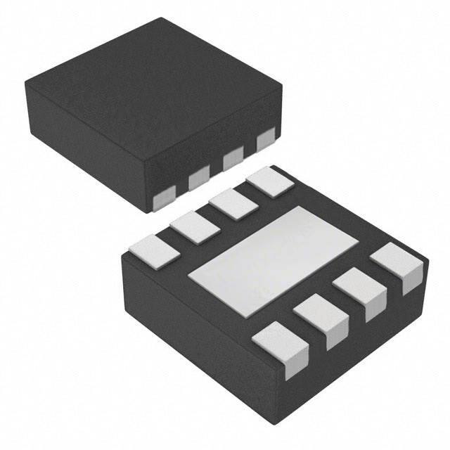


 工商网监
湘ICP备2023018690号
工商网监
湘ICP备2023018690号
