Product
Folder
Sample &
Buy
Tools &
Software
Technical
Documents
Support &
Community
OPA857-DIE
SBOS813 – AUGUST 2016
OPA857-DIE
Ultralow-Noise, Wideband, Selectable-Feedback Resistance Transimpedance Amplifier
1 Features
2 Applications
•
•
•
•
•
•
•
•
1
•
•
•
•
•
Internal Midscale Reference Voltage
Pseudo-Differential Output Voltage
Wide Dynamic Range
Closed-Loop Transimpedance Bandwidth:
– 125 MHz (5-kΩ Transimpedance Gain, 1.5-pF
External Parasitic Capacitance)
– 105 MHz (20-kΩ Transimpedance Gain, 1.5-pF
External Parasitic Capacitance)
Ultralow Input-Referred Current Noise (Brickwall
Filter BW = 135 MHz):
– 15 nARMS (20-kΩ Transimpedance)
Very Fast Overload Recovery Time: < 25 ns
Internal Input Protection Diode
Power Supply:
– Voltage: 2.7 V to 3.6 V
– Current: 23.4 mA
Extended Temperature Range: –40°C to +85°C
Photodiode Monitoring
High-Speed I/V Conversions
Optical Amplifiers
CAT-Scanner Front-Ends
3 Description
The OPA857-DIE is a wideband, fast overdrive
recovery, fast-settling, ultralow-noise transimpedance
amplifier
targeted
at
photodiode
monitoring
applications. With selectable feedback resistance, the
OPA857-DIE simplifies the design of highperformance optical systems. Very fast overload
recovery time and internal input protection provide the
best combination to protect the remainder of the
signal chain from overdrive while minimizing recovery
time. The two selectable transimpedance gain
configurations allow high dynamic range and flexibility
required in modern transimpedance amplifier
applications.
The device is characterized for operation over the full
industrial temperature range from –40°C to +85°C.
Ordering Information (1)
(1)
(2)
PRODUCT
PACKAGE
DESIGNATOR
PACKAGE
OPA857-DIE
TD
Bare die in gel pak VR (2)
ORDERABLE PART NUMBER
PACKAGE QUANTITY
OPA857TD1
324
OPA857TD2
10
For the most current package and ordering information, see the Package Option Addendum at the end of this document, or see the TI
web site at www.ti.com.
Processing is per the Texas Instruments commercial production baseline and is in compliance with the Texas Instruments Quality
Control System in effect at the time of manufacture. Electrical screening consists of DC parametric and functional testing at room
temperature only. Unless otherwise specified by Texas Instruments AC performance and performance over temperature is not
warranted. Visual Inspection is performed in accordance with MIL-STD-883 Test Method 2010 Condition B at 75X minimum.
1
An IMPORTANT NOTICE at the end of this data sheet addresses availability, warranty, changes, use in safety-critical applications,
intellectual property matters and other important disclaimers. PRODUCTION DATA.
�OPA857-DIE
SBOS813 – AUGUST 2016
www.ti.com
This integrated circuit can be damaged by ESD. Texas Instruments recommends that all integrated circuits be handled with
appropriate precautions. Failure to observe proper handling and installation procedures can cause damage.
ESD damage can range from subtle performance degradation to complete device failure. Precision integrated circuits may be more
susceptible to damage because very small parametric changes could cause the device not to meet its published specifications.
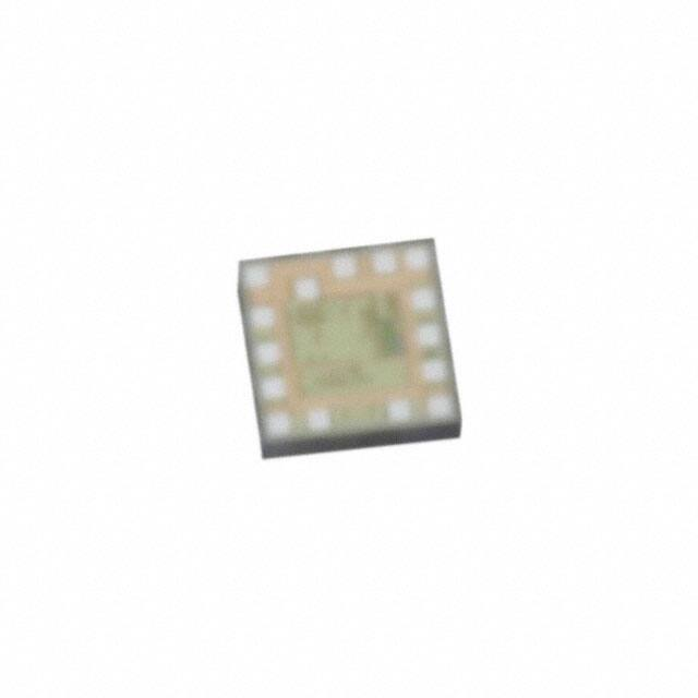
4 Bare Die Information
DIE THICKNESS
BACKSIDE FINISH
BACKSIDE
POTENTIAL
BOND PAD
METALLIZATION COMPOSITION
BOND PAD
THICKNESS
15 mils.
Silicon with backgrind
GND
TiW/AlCu (0.5%)
1100 nm
1
14
13
12
15
2
11
3
10
4
9
5
7
6
807.0
8
0
40
0
40
785.0
2
Submit Documentation Feedback
Copyright © 2016, Texas Instruments Incorporated
Product Folder Links: OPA857-DIE
�OPA857-DIE
www.ti.com
SBOS813 – AUGUST 2016
Bond Pad Coordinates in Microns
NAME
PAD
NUMBER
X MIN
Y MIN
X MAX
Y MAX
GND
1
15
637
90
712
Ground
CTRL
2
15
465
90
540
Control pin for transimpedance gain. GND, logic 0 = 5-kΩ
internal resistance; +VS, logic 1 = 20-kΩ internal resistance.
GND
3
15
315
90
390
Ground
GND
4
15
165
90
240
Ground
OUTN
5
15
15
90
90
Common-mode voltage output reference
GND
6
165
15
240
90
Ground
GND
7
465
15
540
90
Ground
OUT
8
615
15
690
90
Signal output
+VS
9
615
165
690
240
Supply voltage
+VS
10
615
315
690
390
Supply voltage
+VS
11
615
465
690
540
Supply voltage
GND
12
615
637
690
712
Ground
TESD_SD
13
493.7
637
568.7
712
Test mode enable. Connect to GND for normal operation, and
connect to +VS to enable test mode.
TEST_IN
14
343.7
637
418.7
712
Test mode input. Connect to +VS during normal operation.
IN
15
193.7
561.95
268.7
636.95
DESCRIPTION
Input
Submit Documentation Feedback
Copyright © 2016, Texas Instruments Incorporated
Product Folder Links: OPA857-DIE
3
�PACKAGE OPTION ADDENDUM
www.ti.com
24-Apr-2019
PACKAGING INFORMATION
Orderable Device
Status
(1)
Package Type Package Pins Package
Drawing
Qty
Eco Plan
Lead/Ball Finish
MSL Peak Temp
(2)
(6)
(3)
Op Temp (°C)
Device Marking
(4/5)
OPA857TD1
ACTIVE
0
324
TBD
Call TI
Call TI
-40 to 85
OPA857TD2
ACTIVE
0
120
TBD
Call TI
Call TI
-40 to 85
(1)
The marketing status values are defined as follows:
ACTIVE: Product device recommended for new designs.
LIFEBUY: TI has announced that the device will be discontinued, and a lifetime-buy period is in effect.
NRND: Not recommended for new designs. Device is in production to support existing customers, but TI does not recommend using this part in a new design.
PREVIEW: Device has been announced but is not in production. Samples may or may not be available.
OBSOLETE: TI has discontinued the production of the device.
(2)
RoHS: TI defines "RoHS" to mean semiconductor products that are compliant with the current EU RoHS requirements for all 10 RoHS substances, including the requirement that RoHS substance
do not exceed 0.1% by weight in homogeneous materials. Where designed to be soldered at high temperatures, "RoHS" products are suitable for use in specified lead-free processes. TI may
reference these types of products as "Pb-Free".
RoHS Exempt: TI defines "RoHS Exempt" to mean products that contain lead but are compliant with EU RoHS pursuant to a specific EU RoHS exemption.
Green: TI defines "Green" to mean the content of Chlorine (Cl) and Bromine (Br) based flame retardants meet JS709B low halogen requirements of
很抱歉,暂时无法提供与“OPA857TD2”相匹配的价格&库存,您可以联系我们找货
免费人工找货- 国内价格
- 1+120.74990
- 200+100.62500
- 500+80.50000
- 1000+67.08330