Order
Now
Product
Folder
Support &
Community
Tools &
Software
Technical
Documents
OPA859
SBOS852 – SEPTEMBER 2018
OPA859 1.8 GHz Unity-Gain Bandwidth, 3.3-nV/√Hz, FET Input Amplifier
1 Features
3 Description
•
•
•
•
•
•
The OPA859 is a wideband, low-noise operational
amplifier with CMOS inputs for wideband
transimpedance and voltage amplifier applications.
When the device is configured as a transimpedance
amplifier (TIA), the 0.9-GHz gain bandwidth product
(GBWP) enables high closed-loop bandwidths in lowcapacitance photodiode applications.
High Unity-Gain Bandwidth: 1.8 GHz
Gain Bandwidth Product: 900 MHz
Ultra-Low Bias Current MOSFET Inputs: 10 pA
Low Input Voltage Noise: 3.3 nV/√Hz
Slew Rate: 1150 V/µs
Low Input Capacitance:
– Common-Mode: 0.6 pF
– Differential: 0.2 pF
Wide Input Common-Mode Range:
– 1.4 V from Positive Supply
– Includes Negative Supply
2.5 VPP Output Swing in TIA Configuration
Supply Voltage Range: 3.3 V to 5.25 V
Quiescent Current: 20.5 mA
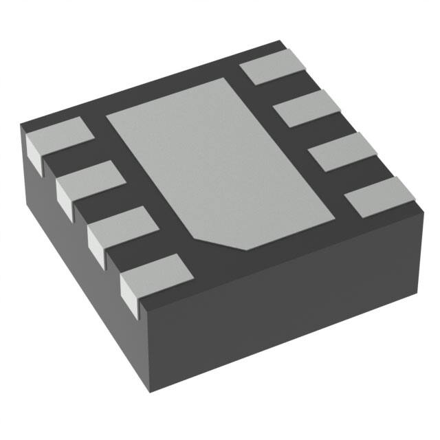
Package: 8-Pin WSON
Temperature Range: –40 to +125°C
•
•
•
•
•
•
2 Applications
•
•
•
•
•
•
•
•
•
High-Speed Transimpedance Amplifier
Laser Distance Measurement
CCD Output Buffer
High-Speed Buffer
Optical Time Domain Reflectometry (OTDR)
High-Speed Active Filter
3D Scanner
Silicon Photomultiplier (SiPM) Buffer Amplifier
Photomultiplier Tube Post Amplifier
High-Speed Time-of-Flight Receiver
The graph below shows the bandwidth and noise
performance of the OPA859 as a function of the
photodiode capacitance when the amplifier is set as a
TIA. The total noise is calculated along a bandwidth
range extending from dc to the calculated frequency,
f, on the left-hand scale. The OPA859 package has a
feedback pin (FB) that simplifies the feedback
network connection between the input and the output.
The OPA859 is optimized to operate in optical timeof-flight (ToF) systems where the OPA859 is used
with time-to-digital converters, such as the TDC7201.
Use the OPA859 to drive a high-speed analog-todigital converter (ADC) in high-resolution LIDAR
systems with a differential output amplifier, such as
the THS4541 or LMH5401.
Device Information(1)
PART NUMBER
OPA859
Photodiode Capacitance vs Bandwidth and Noise
225
RF
5V
TLV3501
±
+
3.5 V
OPA859
+
Stop 2
VREF
±
Start 2
Object
CF
RF
VBIAS
5V
TLV3501
±
TDC7201
(Time-toDigital
Converter)
+
3.5 V
+
OPA859
Stop 1
VREF
±
Start 1
Closed-loop Bandwidth, f-3dB (MHz)
Rx
Lens
BODY SIZE (NOM)
2.00 mm × 2.00 mm
(1) For all available packages, see the package option addendum
at the end of the data sheet.
CF
VBIAS
PACKAGE
WSON (8)
150
f-3dB, RF = 2 k:
f-3dB, RF = 5 k:
IRN, RF = 2 k:
IRN, RF = 5 k:
200
175
135
120
150
105
125
90
100
75
75
60
50
45
25
30
0
0
Tx
Lens
Pulsed Laser
Diode
MSP430
Controller
2
4
6
8
10
12
14
Photodiode capacitance (pF)
16
18
15
20
Integrated Input Referred Noise, IRN (nARMS)
1
D409
1
An IMPORTANT NOTICE at the end of this data sheet addresses availability, warranty, changes, use in safety-critical applications,
intellectual property matters and other important disclaimers. PRODUCTION DATA.
�OPA859
SBOS852 – SEPTEMBER 2018
www.ti.com
Table of Contents
1
2
3
4
5
6
7
Features ..................................................................
Applications ...........................................................
Description .............................................................
Revision History.....................................................
Device Comparison Table.....................................
Pin Configuration and Functions .........................
Specifications.........................................................
1
1
1
2
3
3
4
7.1
7.2
7.3
7.4
7.5
7.6
4
4
4
4
5
7
Absolute Maximum Ratings ......................................
ESD Ratings..............................................................
Recommended Operating Conditions.......................
Thermal Information ..................................................
Electrical Characteristics ..........................................
Typical Characteristics ..............................................
8
Parameter Measurement Information ................ 14
9
Detailed Description ............................................ 15
9.3 Feature Description................................................. 16
9.4 Device Functional Modes........................................ 19
10 Application and Implementation........................ 20
10.1 Application Information.......................................... 20
10.2 Typical Application ............................................... 21
11 Power Supply Recommendations ..................... 23
12 Layout................................................................... 24
12.1 Layout Guidelines ................................................. 24
12.2 Layout Example .................................................... 24
13 Device and Documentation Support ................. 25
13.1
13.2
13.3
13.4
13.5
13.6
13.7
8.1 Parameter Measurement Information ..................... 14
9.1 Overview ................................................................. 15
9.2 Functional Block Diagram ....................................... 15
Device Support......................................................
Documentation Support ........................................
Receiving Notification of Documentation Updates
Community Resources..........................................
Trademarks ...........................................................
Electrostatic Discharge Caution ............................
Glossary ................................................................
25
25
25
25
25
25
25
14 Mechanical, Packaging, and Orderable
Information ........................................................... 26
4 Revision History
2
DATE
REVISION
NOTES
September 2018
*
Initial release.
Submit Documentation Feedback
Copyright © 2018, Texas Instruments Incorporated
Product Folder Links: OPA859
�OPA859
www.ti.com
SBOS852 – SEPTEMBER 2018
5 Device Comparison Table
DEVICE
INPUT TYPE
MINIMUM STABLE
GAIN
VOLTAGE NOISE
(nV/√Hz)
INPUT
CAPACITANCE (pF)
GAIN BANDWIDTH
(GHz)
OPA859
CMOS
1 V/V
3.3
0.8
0.9
OPA858
CMOS
7 V/V
2.5
0.8
5.5
OPA855
Bipolar
7 V/V
0.98
0.8
8
LMH6629
Bipolar
10 V/V
0.69
5.7
4
6 Pin Configuration and Functions
DSG Package
8-Pin WSON With Exposed Thermal Pad
Top View
FB
1
NC
2
8
PD
7
VS+
Thermal pad
IN±
3
6
OUT
IN+
4
5
VS±
Not to scale
Pin Functions
PIN
NAME
NO.
I/O
DESCRIPTION
FB
1
I
Feedback connection to output of amplifier
IN–
3
I
Inverting input
IN+
4
I
Noninverting input
NC
2
—
Do not connect
OUT
6
O
Amplifier output
PD
8
I
Power down connection. PD = logic low = power off mode; PD = logic high = normal operation.
VS–
5
—
Negative voltage supply
VS+
7
—
Positive voltage supply
—
Connect the thermal pad to VS–
Thermal pad
Submit Documentation Feedback
Copyright © 2018, Texas Instruments Incorporated
Product Folder Links: OPA859
3
�OPA859
SBOS852 – SEPTEMBER 2018
www.ti.com
7 Specifications
7.1 Absolute Maximum Ratings
over operating free-air temperature range (unless otherwise noted) (1)
MIN
VS
Total supply voltage (VS+ – VS–)
VIN+, VIN–
Input voltage
VID
Differential input voltage
VOUT
Output voltage
IIN
Continuous input current
IOUT
Continuous output current (2)
TJ
Junction temperature
TA
Operating free-air temperature
Tstg
Storage temperature
(1)
(2)
MAX
(VS–) – 0.5
(VS–) – 0.5
UNIT
5.5
V
(VS+) + 0.5
V
1
V
(VS+) + 0.5
V
±10
mA
±100
mA
150
°C
–40
125
°C
–65
150
°C
Stresses beyond those listed under Absolute Maximum Ratings may cause permanent damage to the device. These are stress ratings
only, which do not imply functional operation of the device at these or any other conditions beyond those indicated under Recommended
Operating Conditions. Exposure to absolute-maximum-rated conditions for extended periods may affect device reliability.
Long-term continuous output current for electromigration limits.
7.2 ESD Ratings
VALUE
V(ESD)
(1)
(2)
Electrostatic discharge
Human-body model (HBM), per ANSI/ESDA/JEDEC JS-001 (1)
±1000
Charged-device model (CDM), per JEDEC specification JESD22-C101 (2)
±1500
UNIT
V
JEDEC document JEP155 states that 500-V HBM allows safe manufacturing with a standard ESD control process.
JEDEC document JEP157 states that 250-V CDM allows safe manufacturing with a standard ESD control process.
7.3 Recommended Operating Conditions
over operating free-air temperature range (unless otherwise noted)
MIN
NOM
MAX
5
5.25
V
125
°C
VS
Total supply voltage (VS+ – VS–)
3.3
TA
Operating free-air temperature
–40
UNIT
7.4 Thermal Information
OPA859
THERMAL METRIC (1)
DSG (WSON)
UNIT
8 PINS
RθJA
Junction-to-ambient thermal resistance
80.1
°C/W
RθJC(top)
Junction-to-case (top) thermal resistance
100
°C/W
RθJB
Junction-to-board thermal resistance
45
°C/W
ψJT
Junction-to-top characterization parameter
6.8
°C/W
ψJB
Junction-to-board characterization parameter
45.2
°C/W
RθJC(bot)
Junction-to-case (bottom) thermal resistance
22.7
°C/W
(1)
4
For more information about traditional and new thermal metrics, see the Semiconductor and IC Package Thermal Metrics application
report.
Submit Documentation Feedback
Copyright © 2018, Texas Instruments Incorporated
Product Folder Links: OPA859
�OPA859
www.ti.com
SBOS852 – SEPTEMBER 2018
7.5 Electrical Characteristics
VS+ = 5 V, VS- = 0 V, input common-mode biased at midsupply, unity gain configuration, RL = 200 Ω, output load is referenced
to midsupply, and TA ≈ +25℃ (unless otherwise noted)
PARAMETER
TEST CONDITIONS
MIN
TYP
MAX
UNIT
AC PERFORMANCE
SSBW
Small-signal bandwidth
VOUT = 100 mVPP
1.8
GHz
LSBW
Large-signal bandwidth
VOUT = 2 VPP
400
MHz
GBWP
Gain-bandwidth product
900
MHz
Bandwidth for 0.1dB flatness
140
MHz
1150
V/µs
SR
Slew rate (10% - 90%)
VOUT = 2-V step
tr
Rise time
VOUT = 100-mV step
0.3
ns
tf
Fall time
VOUT = 100-mV step
0.3
ns
Settling time to 0.1%
VOUT = 2-V step
8
ns
Settling time to 0.001%
VOUT = 2-V step
3000
ns
Overshoot/undershoot
VOUT = 2-V step
7%
HD2
Second-order harmonic distortion
HD3
Third-order harmonic distortion
en
Input-referred voltage noise
ZOUT
Closed-loop output impedance
f = 10 MHz, VOUT = 2 VPP
90
f = 100 MHz, VOUT = 2 VPP
60
f = 10 MHz, VOUT = 2 VPP
86
dBc
f = 100 MHz, VOUT = 2 VPP
64
dBc
f = 1 MHz
3.3
nV/√Hz
f = 1 MHz
0.15
Ω
dBc
DC PERFORMANCE
AOL
Open-loop voltage gain
VOS
Input offset voltage
TA = 25°C
60
65
–5
±0.9
dB
ΔVOS/ΔT
Input offset voltage drift
TA = –40°C to +125°C
IBN, IBI
Input bias current
TA = 25°C
–5
±0.5
5
pA
IBOS
Input offset current
TA = 25°C
–5
±0.1
5
pA
CMRR
Common-mode rejection ratio
VCM = ±0.5 V
70
84
dB
1
GΩ
5
–2
mV
µV/°C
INPUT
Common-mode input resistance
CCM
Common-mode input capacitance
Differential input resistance
CDIFF
Differential input capacitance
VIH
Common-mode input range (high)
VS+ = 3.3 V, CMRR > 66 dB
VIL
Common-mode input range (low)
VS+ = 3.3 V, CMRR > 66 dB
VIH
Common-mode input range (high)
VIL
Common-mode input range (low)
CMRR > 66 dB
1.7
0.62
pF
1
GΩ
0.2
pF
1.9
0
3.4
TA = –40°C to +125°C, CMRR > 66 dB
V
0.4
3.6
V
3.4
CMRR > 66 dB
TA = –40°C to +125°C, CMRR > 66 dB
V
0
0.4
0.35
0.45
V
OUTPUT
VOH
Output voltage (high)
VOH
Output voltage (high)
VOL
Output voltage (low)
VOL
Output voltage (low)
IO_LIN
Linear output drive (sink and source)
ISC
Output short-circuit current
VS+ = 3.3 V, TA = 25°C
TA = 25°C
2.3
2.4
3.95
4.1
TA = –40°C to +125°C
3.9
VS+ = 3.3 V, TA = 25°C
V
V
1.05
1.15
TA = 25°C
1.1
1.15
TA = –40°C to +125°C
1.2
RL = 10 Ω, AOL > 52 dB
65
TA = –40°C to +125°C, RL = 10 Ω,
AOL > 52 dB
105
Submit Documentation Feedback
Copyright © 2018, Texas Instruments Incorporated
Product Folder Links: OPA859
V
76
64
85
V
mA
mA
5
�OPA859
SBOS852 – SEPTEMBER 2018
www.ti.com
Electrical Characteristics (continued)
VS+ = 5 V, VS- = 0 V, input common-mode biased at midsupply, unity gain configuration, RL = 200 Ω, output load is referenced
to midsupply, and TA ≈ +25℃ (unless otherwise noted)
PARAMETER
TEST CONDITIONS
MIN
TYP
MAX
UNIT
POWER SUPPLY
VS+ = 5 V
VS+ = 3.3 V
IQ
Quiescent current
VS+ = 5.25 V
18
20.5
24
17.5
20
23.5
18
21
24
TA = 125°C
mA
24.5
TA = –40°C
18.5
PSRR+
Positive power-supply rejection ratio
66
74
PSRR–
Negative power-supply rejection ratio
64
72
dB
POWER DOWN
Disable voltage threshold
Amplifier OFF below this voltage
Enable voltage threshold
Amplifier ON above this voltage
1
V
1.5
1.8
V
Power-down quiescent current
70
140
µA
PD bias current
70
200
µA
Turnon time delay
Time to VOUT = 90% of final value
Turnoff time delay
6
0.65
Submit Documentation Feedback
25
ns
120
ns
Copyright © 2018, Texas Instruments Incorporated
Product Folder Links: OPA859
�OPA859
www.ti.com
SBOS852 – SEPTEMBER 2018
7.6 Typical Characteristics
3
3
0
0
Normalized Gain (dB)
Normalized Gain (dB)
at TA = 25°C, VS+ = 2.5 V, VS– = –2.5 V, VIN+ = 0 V, Gain = 1 V/V, RF = 0 Ω, RL = 200 Ω, and output load referenced to
midsupply (unless otherwise noted)
-3
-6
Gain = +1 V/V
Gain = 1 V/V
Gain = +2 V/V
Gain = +5 V/V
Gain = +20 V/V
-9
-12
1M
10M
-3
-6
-9
100M
Frequency (Hz)
1G
VS = 3.3 V
VS = 5 V
5G
-12
1M
D300
10M
VOUT = 100 mVPP; see Parameter Measurement Information for
circuit configuration
100M
Frequency (Hz)
1G
5G
D302
VOUT = 100 mVPP
Figure 1. Small-Signal Frequency Response vs Gain
Figure 2. Small-Signal Frequency Response vs Supply
Voltage
2
3
1
0
Normalized Gain (dB)
Normalized Gain (dB)
0
-3
-6
-9
-2
-3
-4
-5
-6
RL = 100 :
RL = 200 :
RL = 400 :
-12
1M
-1
-7
10M
100M
Frequency (Hz)
1G
-8
1M
5G
D303
VOUT = 100 mVPP
100M
Frequency (Hz)
1G
5G
D304
Figure 4. Small-Signal Frequency Response vs Ambient
Temperature
4
3
2
Normalized Gain (dB)
0
Normalized Gain (dB)
10M
VOUT = 100 mVPP
Figure 3. Small-Signal Frequency Response vs Output Load
-3
-6
-9
-12
TA = 125qC
TA = 85qC
TA = 25qC
TA = 0qC
TA = 40qC
VS = r1.65 V, VOUT = 100 mVPP, VCM = 0 V
VS = r2.5 V, VOUT = 100 mVPP, VCM = 0.9 V
VS = r2.5 V, VOUT = 2 VPP, VCM = 0 V
-15
1M
10M
Frequency (Hz)
Gain = 20 V/V
0
-2
-4
-6
-8
-10
-12
1M
100M
D301
RF = 453 Ω
RS = 18 :, CL = 10 pF
RS = 9.1 :, CL = 47 pF
RS = 6.2 :, CL = 100 pF
RS = 2 :, CL = 1 nF
10M
100M
Frequency (Hz)
1G
D305
VOUT = 100 mVPP, See Figure 46 for circuit configuration
Figure 5. Frequency Response at Gain = 20 V/V
Figure 6. Small-Signal Frequency Response vs Capacitive
Load
Submit Documentation Feedback
Copyright © 2018, Texas Instruments Incorporated
Product Folder Links: OPA859
7
�OPA859
SBOS852 – SEPTEMBER 2018
www.ti.com
Typical Characteristics (continued)
at TA = 25°C, VS+ = 2.5 V, VS– = –2.5 V, VIN+ = 0 V, Gain = 1 V/V, RF = 0 Ω, RL = 200 Ω, and output load referenced to
midsupply (unless otherwise noted)
3
0.2
0.1
Normalized Gain (dB)
-3
-6
Gain = +1 V/V
Gain = 1 V/V
Gain = +2 V/V
Gain = +5 V/V
Gain = +20 V/V
-9
-12
1M
0
-0.1
-0.2
-0.3
-0.4
10M
100M
Frequency (Hz)
-0.5
1M
1G
10M
Frequency (Hz)
D306
VOUT = 2 VPP
Figure 7. Large-Signal Frequency Response vs Gain
Figure 8. Large-Signal Response for 0.1-dB Gain Flatness
Open-Loop Magnitude (dB)
Closed-Loop Output Impedance (:)
75
10
1
0.1
0.01
100k
1M
10M
Frequency (Hz)
45
AOL Magnitude (dB)
AOL Phase (q)
60
-45
30
-90
15
-135
0
-180
-15
10k
100M
0
45
-225
100k
1M
10M
100M
Frequency (Hz)
D309
Small-Signal Response
1G
D310
Small-Signal Response
Figure 9. Closed-Loop Output Impedance vs Frequency
Figure 10. Open-Loop Magnitude and Phase vs Frequency
4
Input Referred Voltage Noise (nV/—Hz)
100
Input Referred Voltage Noise (nV/—Hz)
D307
VOUT = 2 VPP
100
10
1
1k
100M
Open-Loop Phase (q)
Normalized Gain (dB)
0
10k
100k
1M
Frequency (Hz)
10M
100M
3.8
3.6
3.4
3.2
3
2.8
2.6
-40
D311
-20
0
20
40
60
80
100
Ambient Temperature (qC)
120
140
D312
Frequency 10 MHz
Figure 11. Voltage Noise Density vs Frequency
8
Figure 12. Voltage Noise Density vs Ambient Temperature
Submit Documentation Feedback
Copyright © 2018, Texas Instruments Incorporated
Product Folder Links: OPA859
�OPA859
www.ti.com
SBOS852 – SEPTEMBER 2018
Typical Characteristics (continued)
at TA = 25°C, VS+ = 2.5 V, VS– = –2.5 V, VIN+ = 0 V, Gain = 1 V/V, RF = 0 Ω, RL = 200 Ω, and output load referenced to
midsupply (unless otherwise noted)
-40
-60
-70
-80
-90
-100
-110
-120
1M
10M
Frequency (Hz)
-80
-90
-100
10M
Frequency (Hz)
D313
HD2, RL = 100 :
HD2, RL = 200 :
HD2, RL = 400 :
-70
-80
-90
-100
-110
HD3, RL = 100 :
HD3, RL = 200 :
HD3, RL = 400 :
-60
-70
-80
-90
-100
-110
10M
Frequency (Hz)
-120
1M
100M
10M
Frequency (Hz)
D315
VOUT = 2 VPP
Figure 15. Harmonic Distortion (HD2) vs Output Load
Figure 16. Harmonic Distortion (HD3) vs Output Load
HD2, Gain = 1 V/V, RF = 0 :
HD2, Gain = 1 V/V, RF = 150 :
HD2, Gain = 2 V/V, RF = 150 :
HD2, Gain = 5 V/V, RF = 453 :
HD3, Gain = 1 V/V, RF = 0 :
HD3, Gain = 1 V/V, RF = 150 :
HD3, Gain = 2 V/V, RF = 150 :
HD3, Gain = 5 V/V, RF = 453 :
-50
Harmonic Distortion (dBc)
Harmonic Distortion (dBc)
D316
-40
-70
-80
-90
-100
-110
-120
1M
100M
VOUT = 2 VPP
-40
-60
D314
Figure 14. Harmonic Distortion (HD3) vs Output Swing
-50
-60
-50
100M
-40
Harmonic Distortion (dBc)
Harmonic Distortion (dBc)
-70
-120
1M
100M
Figure 13. Harmonic Distortion (HD2) vs Output Swing
-120
1M
-60
-110
-40
-50
HD3, VOUT = 0.5 VPP
HD3, VOUT = 1 VPP
HD3, VOUT = 2 VPP
HD3, VOUT = 2.5 VPP
-50
Harmonic Distortion (dBc)
Harmonic Distortion (dBc)
-50
-40
HD2, VOUT = 0.5 VPP
HD2, VOUT = 1 VPP
HD2, VOUT = 2 VPP
HD2, VOUT = 2.5 VPP
-60
-70
-80
-90
-100
-110
10M
Frequency (Hz)
100M
-120
1M
10M
Frequency (Hz)
D317
VOUT = 2 VPP
100M
D318
VOUT = 2 VPP
Figure 17. Harmonic Distortion (HD2) vs Gain
Figure 18. Harmonic Distortion (HD3) vs Gain
Submit Documentation Feedback
Copyright © 2018, Texas Instruments Incorporated
Product Folder Links: OPA859
9
�OPA859
SBOS852 – SEPTEMBER 2018
www.ti.com
Typical Characteristics (continued)
at TA = 25°C, VS+ = 2.5 V, VS– = –2.5 V, VIN+ = 0 V, Gain = 1 V/V, RF = 0 Ω, RL = 200 Ω, and output load referenced to
midsupply (unless otherwise noted)
60
1.25
Input
Output
0.75
Voltage Swing (V)
Voltage Swing (mV)
40
Input
Output
1
20
0
-20
0.5
0.25
0
-0.25
-0.5
-0.75
-40
-1
-60
-1.25
Time (5 ns/div)
Time (5 ns/div)
D319
Average Rise and Fall Time (10% - 90%) = 450 ps
Figure 19. Small-Signal Transient Response
Figure 20. Large-Signal Transient Response
4
0.075
3
0.05
2
Voltage Swing (V)
Voltage Swing (mV)
D320
Slew Rate: Falling = 1160 V/µs, Rising = 1400 V/µs
0.025
0
-0.025
-0.05
RS = 18 :, CL = 10 pF
RS = 9.1 :, CL = 47 pF
RS = 6.2 :, CL = 100 pF
RS = 2 :, CL = 1 nF
1
0
-1
-2
-3
Ideal Output
Measured Output
-4
-0.075
Time (10 ns/div)
Time (5 ns/div)
D322
D321
See Figure 46 for circuit configuration
Gain = 5 V/V, RF = 453 Ω, 2x Output Overdrive
Figure 21. Small-Signal Transient Response vs Capacitive
Load
Figure 22. Output Overload Response
3
3
2
Voltage Swing (V)
2
Voltage Swing (V)
Power Down (PD)
Output
1
0
-1
1
0
-1
-2
-2
Power Down (PD)
Output
-3
-3
Time (5 ns/div)
Time (5 ns/div)
D324
D323
Figure 23. Turnon Transient Response
10
Submit Documentation Feedback
Figure 24. Turnoff Transient Response
Copyright © 2018, Texas Instruments Incorporated
Product Folder Links: OPA859
�OPA859
www.ti.com
SBOS852 – SEPTEMBER 2018
Typical Characteristics (continued)
at TA = 25°C, VS+ = 2.5 V, VS– = –2.5 V, VIN+ = 0 V, Gain = 1 V/V, RF = 0 Ω, RL = 200 Ω, and output load referenced to
midsupply (unless otherwise noted)
80
CMRR
Power Supply Rejection Ratio (dB)
Common-Mode Rejection Ratio (dB)
100
80
60
40
20
0
10k
100k
1M
10M
Frequency (Hz)
100M
PSRR+
PSRR
60
40
20
0
-20
10k
1G
100k
1M
10M
Frequency (Hz)
D325
Small-Signal Response
100M
1G
D326
Small-Signal Response
Figure 25. Common-Mode Rejection Ratio vs Frequency
Figure 26. Power Supply Rejection Ratio vs Frequency
24
21.5
23
21
Quiescent Current (mA)
Quiescent Current (mA)
21.25
20.75
20.5
20.25
20
19.75
19.5
22
21
20
19
Unit 1
Unit 2
Unit 1
Unit 2
19.25
18
-40
19
3
3.25
3.5
3.75
4
4.25 4.5
Total Supply Voltage (V)
4.75
5
5.25
2 Typical Units
Figure 27. Quiescent Current vs Supply Voltage
1
78
0.75
76
0.5
74
72
70
20
40
60
80
100
Ambient Temperature (qC)
120
140
D361
2 Typical Units
Figure 28. Quiescent Current vs Ambient Temperature
Offset Voltage (mV)
Quiescent Current (PA)
0
VS = 5 V
80
Unit 1
Unit 2
Unit 3
0.25
0
-0.25
68
-0.5
66
-0.75
64
-40
-20
D360
-1
-20
0
20
40
60
80
100
Ambient Temperature (qC)
120
140
3
3.25
D362
32 Units Tested
3.5
3.75
4
4.25 4.5
Total Supply Voltage (V)
4.75
5
5.25
D363
3 Typical Units
Figure 29. Quiescent Current (Amplifier Disabled) vs
Ambient Temperature
Figure 30. Offset Voltage vs Supply Voltage
Submit Documentation Feedback
Copyright © 2018, Texas Instruments Incorporated
Product Folder Links: OPA859
11
�OPA859
SBOS852 – SEPTEMBER 2018
www.ti.com
Typical Characteristics (continued)
at TA = 25°C, VS+ = 2.5 V, VS– = –2.5 V, VIN+ = 0 V, Gain = 1 V/V, RF = 0 Ω, RL = 200 Ω, and output load referenced to
midsupply (unless otherwise noted)
2
0.8
Unit 1
Unit 2
Unit 3
1.5
0.4
Offset Voltage (mV)
Offset Voltage (mV)
0.6
0.2
0
-0.2
1
0.5
0
-0.4
-0.5
-0.6
-0.8
-40
-1
-20
0
20
40
60
80
100
Ambient Temperature (qC)
µ = –2.1 µV/°C
σ = 2 µV/°C
120
140
0
32 Units Tested
1
1.5
2
2.5
3
3.5
Common-Mode Voltage (V)
VS = 5 V
Figure 31. Offset Voltage vs Ambient Temperature
4
4.5
D366
3 Typical Units
Figure 32. Offset Voltage vs Input Common-Mode Voltage
5
1.5
TA = -40qC
TA = +25qC
TA = +125qC
4
3
1
Offset Voltage (mV)
Offset Voltage (mV)
0.5
D364
0.5
2
1
0
-1
-2
0
-3
Unit 1
Unit 2
Unit 3
-4
-5
-0.5
0
0.5
1
1.5
2
2.5
3
Common-Mode Voltage
3.5
4
1
4.5
1.5
2
D367
VS = 5 V
VS = 5 V
Figure 33. Offset Voltage vs Input Common-Mode Voltage
vs Ambient Temperature
2.5
3
Output Voltage (V)
3.5
4
4.5
D369
3 Typical Units
Figure 34. Offset Voltage vs Output Swing
10n
4
3
Input Bias Current (A)
Offset Voltage (mV)
1n
2
1
100p
0
-1
-2
1p
TA = -40qC
TA = +25qC
TA = +125qC
-3
-4
1
1.5
2
2.5
3
Output Voltage (V)
3.5
4
10p
4.5
0.1p
-40
D370
VS = 5 V
-20
0
20
40
60
80
100
Ambient Temperature (qC)
120
140
D371
3 Typical Units
Figure 35. Offset Voltage vs Output Swing vs Ambient
Temperature
12
Unit 1
Unit 2
Unit 3
Figure 36. Input Bias Current vs Ambient Temperature
Submit Documentation Feedback
Copyright © 2018, Texas Instruments Incorporated
Product Folder Links: OPA859
�OPA859
www.ti.com
SBOS852 – SEPTEMBER 2018
Typical Characteristics (continued)
at TA = 25°C, VS+ = 2.5 V, VS– = –2.5 V, VIN+ = 0 V, Gain = 1 V/V, RF = 0 Ω, RL = 200 Ω, and output load referenced to
midsupply (unless otherwise noted)
5
2.4
TA = -40qC
TA = +25qC
TA = +125qC
0
2.2
Output Voltage (V)
Input Bias Current (pA)
-5
-10
-15
-20
-25
-30
-35
-40
2
1.8
1.6
1.4
1.2
-45
-50
0
0.5
1
1.5
2
2.5
3
Common-Mode Voltage (V)
3.5
1
-120
4
-100
-80
-60
-40
Output Current (mA)
D372
VS = 5 V
-20
0
D373
VS = 5 V
Figure 37. Input Bias Current vs Input Common-Mode
Voltage
Figure 38. Output Swing vs Sinking Current
4.5
7000
4
6000
Amplifiers (Count)
3
2.5
2
1.5
TA = -40qC
TA = +25qC
TA = +125qC
3000
2000
D374
µ = 20.8 mA
Figure 39. Output Swing vs Sourcing Current
σ = 0.25 mA
24
23.5
23
D340
Quiescent Current (mA)
VS = 5 V
9150 Units Tested
Figure 40. Quiescent Current Distribution
2000
4500
1750
4000
3500
2000
Offset Voltage (mV)
µ = –0.38 mV
σ = 0.97 mV
D341
9150 Units Tested
D342
Input Bias Current (pA)
µ = –0.55 pA
Figure 41. Offset Voltage Distribution
σ = 0.23 pA
9150 Units Tested
Figure 42. Input Bias Current Distribution
Submit Documentation Feedback
Copyright © 2018, Texas Instruments Incorporated
Product Folder Links: OPA859
1.5
1.25
1
0.5
0.75
0
0.25
0
0
500
-0.25
250
-5
-4.5
-4
-3.5
-3
-2.5
-2
-1.5
-1
-0.5
0
0.5
1
1.5
2
2.5
3
3.5
4
4.5
5
1000
-0.5
1500
500
-0.75
750
2500
-1
1000
3000
-1.25
1250
-1.5
Amplifiers (Count)
1500
Amplifiers (Count)
22.5
120
22
100
21.5
40
60
80
Output Current (mA)
21
20
20.5
0
0
20
0
19.5
1000
19
0.5
4000
18.5
1
5000
18
Output Voltage (V)
3.5
13
�OPA859
SBOS852 – SEPTEMBER 2018
www.ti.com
8 Parameter Measurement Information
8.1 Parameter Measurement Information
The various test setup configurations for the OPA859 are shown in the figures below. When configuring the
OPA859 as a noninverting amplifier in gains less 3 V/V, set RF = 150 Ω. When configuring the OPA859 as a
noninverting amplifier in gains of 4 V/V and greater, set RF = 453 Ω.
GND
50
2.5 V
50
50Source
169
+
±
í2.5 V
50
71.5
50Measurement
System
GND
GND
Figure 43. Unity-Gain Buffer Configuration
2.5 V
50
50Source
169
+
50Measurement
System
±
í2.5 V
RG
50
71.5
GND
RF
GND
GND
RG values depend on gain configuration
Figure 44. Noninverting Configuration
2.5 V
169
+
GND
50Source
50Measurement
System
±
í2.5 V
50
150
50
71.5
GND
150
GND
75
GND
Figure 45. Inverting Configuration (Gain = –1 V/V)
GND
50
50Source
2.5 V
50
+
RS
169
±
í2.5 V
CL
GND
50
75
50Measurement
System
GND
GND
Figure 46. Capacitive Load Driver Configuration
14
Submit Documentation Feedback
Copyright © 2018, Texas Instruments Incorporated
Product Folder Links: OPA859
�OPA859
www.ti.com
SBOS852 – SEPTEMBER 2018
9 Detailed Description
9.1 Overview
The ultra-wide, 900-MHz gain bandwidth product (GBWP) of the OPA859, combined with the broadband voltage
noise of 3.3 nV/√Hz, produces a viable amplifier for wideband transimpedance applications, high-speed data
acquisition systems, and applications with weak signal inputs that require low-noise and high-gain front ends.
The OPA859 combines multiple features to optimize dynamic performance. In addition to the wide small-signal
bandwidth, the OPA859 has 400 MHz of large-signal bandwidth (VOUT = 2 VPP), and a slew rate of 1150 V/µs.
The OPA859 is offered in a 2-mm × 2-mm, 8-pin WSON package that features a feedback (FB) pin for a simple
feedback network connection between the amplifiers output and inverting input. Excess capacitance on an
amplifiers input pin can reduce phase margin causing instability. This problem is exacerbated in the case of very
wideband amplifiers like the OPA859. To reduce the effects of stray capacitance on the input node, the OPA859
pinout features an isolation pin (NC) between the feedback and inverting input pins that increases the physical
spacing between them thereby reducing parasitic coupling at high frequencies. The OPA859 also features a very
low capacitance input stage with only 0.8-pF of total input capacitance.
9.2 Functional Block Diagram
The OPA859 is a classic, voltage feedback operational amplifier (op amp) with two high-impedance inputs and a
low-impedance output. Standard application circuits are supported, like the two basic options shown in Figure 47
and Figure 48. The DC operating point for each configuration is level-shifted by the reference voltage (VREF),
which is typically set to midsupply in single-supply operation. VREF is typically connected to ground in split-supply
applications.
VSIG
VS+
VREF
VIN
(1 + RF / RG) × VSIG
+
VOUT
VREF
±
RG
VS±
VREF
RF
Figure 47. Noninverting Amplifier
VS+
VREF
VSIG
VREF
±(RF / RG) × VSIG
+
VOUT
VIN
RG
VREF
±
VS±
RF
Figure 48. Inverting Amplifier
Submit Documentation Feedback
Copyright © 2018, Texas Instruments Incorporated
Product Folder Links: OPA859
15
�OPA859
SBOS852 – SEPTEMBER 2018
www.ti.com
9.3 Feature Description
9.3.1 Input and ESD Protection
The OPA859 is fabricated on a low-voltage, high-speed, BiCMOS process. The internal, junction breakdown
voltages are low for these small geometry devices, and as a result, all device pins are protected with internal
ESD protection diodes to the power supplies as Figure 49 shows. There are two antiparallel diodes between the
inputs of the amplifier that clamp the inputs during an overrange or fault condition.
VS+
Power Supply
ESD Cell
VIN+
+
VOUT
±
VINí
FB
VSí
Figure 49. Internal ESD Structure
9.3.2 Feedback Pin
The OPA859 pin layout is optimized to minimize parasitic inductance and capacitance, which is critical in highspeed analog design. The FB pin (pin 1) is internally connected to the output of the amplifier. The FB pin is
separated from the inverting input of the amplifier (pin 3) by a no connect (NC) pin (pin 2). The NC pin must be
left floating. There are two advantages to this pin layout:
1. A feedback resistor (RF) can connect between the FB and IN– pin on the same side of the package (see
Figure 50) rather than going around the package.
2. The isolation created by the NC pin minimizes the capacitive coupling between the FB and IN– pins by
increasing the physical separation between the pins.
RF
FB 1
8
PD
NC 2
7
VS+
6
OUT
5
VS±
±
+
IN± 3
IN+ 4
Figure 50. RF Connection Between FB and IN– Pins
16
Submit Documentation Feedback
Copyright © 2018, Texas Instruments Incorporated
Product Folder Links: OPA859
�OPA859
www.ti.com
SBOS852 – SEPTEMBER 2018
Feature Description (continued)
9.3.3 Wide Gain-Bandwidth Product
Figure 10 shows the open-loop magnitude and phase response of the OPA859. Calculate the gain bandwidth
product of any op amp by determining the frequency at which the AOL is 40 dB and multiplying that frequency by
a factor of 100. The open-loop response shows the OPA859 to have approximately 63° of phase-margin when
configured as a unity-gain buffer.
Figure 51 shows the open-loop magnitude (AOL) of the OPA859 as a function of temperature. The results show
approximately 5° of phase-margin variation over the entire temperature range. Semiconductor process variation
is the naturally occurring variation in the attributes of a transistor (Early-voltage, β, channel-length and width) and
other passive elements (resistors and capacitors) when fabricated into an integrated circuit. The process
variation can occur across devices on a single wafer, or, across devices over multiple wafer lots over time.
Typically the variation across a single wafer is tightly controlled. Figure 52 shows the AOL magnitude of the
OPA859 as a function of process variation over time. The results show the AOL curve for the nominal process
corner and the variation one standard deviation from the nominal. The simulated results show less than 2° of
phase-margin difference within a standard deviation of process variation when the amplifier is configured as a
unity-gain bufffer.
75
75
AOL at 40qC
AOL at 25qC
AOL at +125qC
45
30
15
0
-15
100k
AOL ( V)
AOL (Typ.)
AOL ( V)
60
Open-Loop Gain (dB)
Open-Loop Gain (dB)
60
45
30
15
0
1M
10M
100M
Frequency (Hz)
-15
100k
1G
D404
Figure 51. Open-Loop Gain vs Temperature
1M
10M
100M
Frequency (Hz)
1G
D405
Figure 52. Open-Loop Gain vs Process Variation
Submit Documentation Feedback
Copyright © 2018, Texas Instruments Incorporated
Product Folder Links: OPA859
17
�OPA859
SBOS852 – SEPTEMBER 2018
www.ti.com
Feature Description (continued)
9.3.4 Slew Rate and Output Stage
In addition to wide bandwidth, the OPA859 features a high slew rate of 1150 V/µs. The slew rate is a critical
parameter in high-speed pulse applications with narrow sub-10-ns pulses, such as optical time-domain
reflectometry (OTDR) and LIDAR. The high slew rate of the OPA859 implies that the device accurately
reproduces a 2-V, sub-ns pulse edge, as seen in Figure 20. The wide bandwidth and slew rate of the OPA859
make it an excellent amplifier for high-speed, signal-chain front ends.
Figure 53 shows the open-loop output impedance of the OPA859 as a function of frequency. To achieve high
slew rates and low output impedance across frequency, the output swing of the OPA859 is limited to
approximately 3 V. The OPA859 is typically used in conjunction with high-speed pipeline ADCs and flash ADCs
that have limited input ranges. Therefore, the OPA859 output swing range coupled with the class-leading voltage
noise specification for a CMOS amplifier maximizes the overall dynamic range of the signal chain.
Open-Loop Output Impedance (ohms)
20
18
16
14
12
10
8
6
4
2
0
10k
100k
1M
10M
100M
Frequency (Hz)
1G
10G
D601
Figure 53. Open-Loop Output Impedance (ZOL) vs Frequency
9.3.5 Current Noise
The input impedance of CMOS and JFET input amplifiers at low frequencies exceed several GΩs. However, at
higher frequencies, the transistors parasitic capacitance to the drain, source, and substrate reduces the
impedance. The high impedance at low frequencies eliminates any bias current and the associated shot noise. At
higher frequencies, the input current noise increases (see Figure 54) as a result of capacitive coupling between
the CMOS gate oxide and the underlying transistor channel. This phenomenon is a natural artifact of the
construction of the transistor and is unavoidable.
100p
Current Noise (A/—Hz)
10p
1p
100f
10f
1f
1k
10k
100k
1M
10M
Frequency (Hz)
100M
1G
D607
Figure 54. Input Current Noise (IBN and IBI) vs Frequency
18
Submit Documentation Feedback
Copyright © 2018, Texas Instruments Incorporated
Product Folder Links: OPA859
�OPA859
www.ti.com
SBOS852 – SEPTEMBER 2018
9.4 Device Functional Modes
9.4.1 Split-Supply and Single-Supply Operation
The OPA859 can be configured with single-sided supplies or split-supplies as shown in Figure 60. Split-supply
operation using balanced supplies with the input common-mode set to ground eases lab testing because most
signal generators, network analyzers, spectrum analyzers, and other lab equipment typically reference inputs and
outputs to ground. Split-supply operation is preferred in systems where the signals swing around ground.
However, the system requires two supply rails. In split-supply operation, the thermal pad must be connected to
the negative supply.
Newer systems use a single power supply to improve efficiency and reduce the cost of the extra power supply.
The OPA859 can be used with a single positive supply (negative supply at ground) with no change in
performance if the input common-mode and output swing are biased within the linear operation of the device. In
single-supply operation, level shift the dc input and output reference voltages by half the difference between the
power supply rails. This configuration maintains the input common-mode and output load reference at midsupply.
To eliminate gain errors, the source driving the reference input common-mode voltage must have low output
impedance across the frequency range of interest . In this case, the thermal pad must be connected to ground.
9.4.2 Power-Down Mode
The OPA859 features a power-down mode to reduce the quiescent current to conserve power. Figure 23 and
Figure 24 show the transient response of the OPA859 as the PD pin toggles between the disabled and enabled
states.
The PD disable and enable threshold voltages are with reference to the negative supply. If the amplifier is
configured with the positive supply at 3.3 V and the negative supply at ground, then the disable and enable
threshold voltages are 0.65 V and 1.8 V, respectively. If the amplifier is configured with ±1.65-V supplies, then
the disable and enable threshold voltages are at –1 V and 0.15 V, respectively. If the amplifier is configured with
±2.5-V supplies, then the threshold voltages are at –1.85 V and –0.7 V.
25
25
20
20
Quiescent Current (mA)
Quiescent Current (mA)
Figure 55 shows the switching behavior of a typical amplifier as the PD pin is swept down from the enabled state
to the disabled state. Similarly, Figure 56 shows the switching behavior of a typical amplifier as the PD pin is
swept up from the disabled state to the enabled state. The small difference in the switching thresholds between
the down sweep and the up sweep is caused by the hysteresis designed into the amplifier to increase immunity
to noise on the PD pin.
15
10
5
15
10
5
TA = -40qC
TA = 25qC
TA = 125qC
0
TA = -40qC
TA = 25qC
TA = 125qC
0
-2
-1.5
-1
-0.5
0
0.5
Power Down Voltage (V)
1
1.5
2
-2
D200
Figure 55. Switching Threshold (PD Pin Swept from HIGH
to LOW)
-1.5
-1
-0.5
0
0.5
Power Down Voltage (V)
1
1.5
2
D201
Figure 56. Switching Threshold (PD Pin Swept from LOW
to HIGH)
Connecting the PD pin low disables the amplifier and places the output in a high-impedance state. When the
amplifier is configured as a noninverting amplifier, the feedback (RF) and gain (RG) resistor network form a
parallel load to the output of the amplifier. To protect the input stage of the amplifier, the OPA859 uses internal,
back-to-back protection diodes between the inverting and noninverting input pins as Figure 49 shows. In the
power-down state, if the differential voltage between the input pins of the amplifier exceeds a diode voltage drop,
an additional low-impedance path is created between the noninverting input pin and the output pin.
Submit Documentation Feedback
Copyright © 2018, Texas Instruments Incorporated
Product Folder Links: OPA859
19
�OPA859
SBOS852 – SEPTEMBER 2018
www.ti.com
10 Application and Implementation
NOTE
Information in the following applications sections is not part of the TI component
specification, and TI does not warrant its accuracy or completeness. TI’s customers are
responsible for determining suitability of components for their purposes. Customers should
validate and test their design implementation to confirm system functionality.
10.1 Application Information
The OPA859 offers high input impedance, very high-bandwidth, high slew-rate, low noise, and better than –60
dBc of distortion performance at frequencies up to 100 MHz. These features make this device an excellent frontend buffer in high-speed data acquisition systems. The wide bandwidth also makes this amplifier an excellent
choice for high-gain active filter systems.
20
Submit Documentation Feedback
Copyright © 2018, Texas Instruments Incorporated
Product Folder Links: OPA859
�OPA859
www.ti.com
SBOS852 – SEPTEMBER 2018
10.2 Typical Application
Figure 57 shows the OPA859 configured as a transimpedance amplifier (U1) in a wide-bandwidth, optical frontend system. A second OPA859 configured as a unity-gain buffer (U2) sets a dc offset voltage to the THS4520.
The THS4520 is used to convert the single-ended transimpedance output of the OPA859 into a differential output
signal. The THS4520 drives the input of the ADS54J64, 14-bit, 1-GSPS analog-to-digital converter (ADC) that
digitizes the analog signal.
CF
VBIAS
RF
5V
3.5 V
±
U1
+
499
OPA859
VOCM = 1.3 V
5V
2.95 V
±
U2
+
OPA859
499
499
5V
+ ±
± +
Low-pass
filter
ADS54J64
499
Figure 57. OPA859 as Both a TIA and a Buffer in an Optical Front-End System
10.2.1 Design Requirements
The objective is to design a low noise, wideband optical front-end system using the OPA859 as a
transimpedance amplifier. The design requirements are:
• Amplifier supply voltage: 5 V
• TIA common-mode voltage: 3.5 V
• THS4520 gain: 1 V/V
• ADC input common-mode voltage: 1.3 V
• ADC analog differential input range: 1.1 VPP
10.2.2 Detailed Design Procedure
The OPA859 meets the growing demand for wideband, low-noise photodiode amplifiers. The closed-loop
bandwidth of a transimpedance amplifier is a function of the following:
1. The total input capacitance (CIN). This total includes the photodiode capacitance, the input capacitance of the
amplifier (common-mode and differential capacitance) and any stray capacitance from the PCB.
2. The op amp gain bandwidth product (GBWP).
3. The transimpedance gain (RF).
Figure 57 shows the OPA859 configured as a TIA, with the avalanche photodiode (APD) reverse biased so that
the APD cathode is tied to a large positive bias voltage. In this configuration, the APD sources current into the op
amp feedback loop so that the output swings in a negative direction relative to the input common-mode voltage.
To maximize the output swing in the negative direction, the OPA859 common-mode voltage is set close to the
positive limit; only 1.5 V from the positive supply rail. The feedback resistance (RF) and the input capacitance
(CIN) form a zero in the noise gain that results in instability if left unchecked. To counteract the effect of the zero,
a pole is inserted into the noise gain transfer function by adding the feedback capacitor (CF).
The Transimpedance Considerations for High-Speed Amplifiers Application Report discusses theories and
equations that show how to compensate a transimpedance amplifier for a particular transimpedance gain and
input capacitance. The bandwidth and compensation equations from the application report are available in an
Excel™ calculator. What You Need To Know About Transimpedance Amplifiers – Part 1 provides a link to the
calculator.
Submit Documentation Feedback
Copyright © 2018, Texas Instruments Incorporated
Product Folder Links: OPA859
21
�OPA859
SBOS852 – SEPTEMBER 2018
www.ti.com
Typical Application (continued)
The equations and calculators in the referenced application report and blog posts are used to model the
bandwidth (f–3dB) and noise (IRN) performance of the OPA859 configured as a TIA. The resultant performance is
shown in Figure 58 and Figure 59. The left-side Y-axis shows the closed-loop bandwidth performance, whereas
the right side of the graph shows the integrated input-referred noise. The noise bandwidth to calculate IRN for a
fixed RF and CPD is set equal to the f–3dB frequency. Figure 58 shows the amplifier performance as a function of
photodiode capacitance (CPD) for RF = 10 kΩ and 20 kΩ. Increasing CPD decreases the closed-loop bandwidth.
To maximize bandwidth, make sure to reduce any stray parasitic capacitance from the PCB. The OPA859 is
designed with 0.8 pF of total input capacitance to minimize the effect of stray capacitance on system
performance. Figure 59 shows the amplifier performance as a function of RF for CPD = 1 pF and 2 pF. Increasing
RF results in lower bandwidth. To maximize the signal-to-noise ratio (SNR) in an optical front-end system,
maximize the gain in the TIA stage. Increasing RF by a factor of X increases the signal level by X, but only
increases the resistor noise contribution by √X, thereby improving SNR.
The OPA859 configured as a unity-gain buffer drives a dc offset voltage of 2.95 V into the lower half of the
THS4520. To maximize the dynamic range of the ADC, the two OPA859 amplifiers drive a differential commonmode of 3.5 V and 2.95 V into the THS4520. The dc offset voltage of the buffer amplifier can be derived using
Equation 1.
VBUF _ DC
VTIA _ CM
§
¨
¨ 1 u VADC _ DIFF _ IN
¨2
§ RF ·
¨
¨
¸
¨
© RG ¹
©
·
¸
¸
¸
¸
¸
¹
where
•
•
•
VTIA_CM is the common-mode voltage of the TIA (3.5 V)
VADC_DIFF_IN is the differential input voltage range of the ADC (1.1 VPP)
RF and RG are the feedback resistance (499 Ω) and gain resistance (499 Ω) of the THS4520 differential
amplifier
(1)
The low-pass filter between the THS4520 and the ADC54J64 minimizes high-frequency noise and maximizes
SNR. The ADC54J64 has an internal buffer that isolates the output of the THS4520 from the ADC samplingcapacitor input, so a traditional charge bucket filter is not required.
200
175
135
120
150
105
125
90
100
75
75
60
50
45
25
30
0
0
2
4
6
8
10
12
14
Photodiode capacitance (pF)
16
18
15
20
140
f-3dB, CF = 0.5 pF
f-3dB, CF = 1 pF
120
IRN, CF = 0.5 pF
IRN, RF = 1 pF
100
300
250
200
80
150
60
100
40
50
20
0
1
D409
Figure 58. Bandwidth and Noise vs Photodiode
Capacitance
22
350
10
Feedback Resistance (k:)
0
100
Integrated Input Referred Noise, IRN (nARMS)
150
f-3dB, RF = 2 k:
f-3dB, RF = 5 k:
IRN, RF = 2 k:
IRN, RF = 5 k:
Closed-loop Bandwidth, f-3dB (MHz)
Closed-loop Bandwidth, f-3dB (MHz)
225
Integrated Input Referred Noise, IRN (nARMS)
10.2.3 Application Curves
D410
Figure 59. Bandwidth and Noise vs Feedback Resistance
Submit Documentation Feedback
Copyright © 2018, Texas Instruments Incorporated
Product Folder Links: OPA859
�OPA859
www.ti.com
SBOS852 – SEPTEMBER 2018
11 Power Supply Recommendations
The OPA859 operates on supplies from 3.3 V to 5.25 V. The OPA859 operates on single-sided supplies, split
and balanced bipolar supplies, and unbalanced bipolar supplies. Because the OPA859 does not feature rail-torail inputs or outputs, the input common-mode and output swing ranges are limited at 3.3-V supplies.
a) Single supply configuration
VS+
VS+
2
+
0.1 …F
RG
75
6.8 …F
RF
453
±
50-Ÿ 6RXUFH
+
VI
200
RT
49.9
VS+
2
VS+
2
b) Split supply configuration
VS+
+
0.1 …F
RG
75
6.8 …F
RF
453
±
50-Ÿ 6RXUFH
+
VI
200
+
RT
49.9
0.1 …F
6.8 …F
VS±
Figure 60. Split and Single Supply Circuit Configuration , Gain = 7 V/V
Submit Documentation Feedback
Copyright © 2018, Texas Instruments Incorporated
Product Folder Links: OPA859
23
�OPA859
SBOS852 – SEPTEMBER 2018
www.ti.com
12 Layout
12.1 Layout Guidelines
Achieving optimum performance with a high-frequency amplifier like the OPA859 requires careful attention to
board layout parasitics and external component types. Recommendations that optimize performance include:
• Minimize parasitic capacitance from the signal I/O pins to ac ground. Parasitic capacitance on the output
and inverting input pins can cause instability. To reduce unwanted capacitance, cut out the power and ground
traces under the signal input and output pins. Otherwise, ground and power planes must be unbroken
elsewhere on the board. When configuring the amplifier as a TIA, if the required feedback capacitor is less
than 0.15 pF, consider using two series resistors, each of half the value of a single resistor in the feedback
loop to minimize the parasitic capacitance from the resistor.
• Minimize the distance (less than 0.25") from the power-supply pins to high-frequency bypass
capacitors. Use high-quality, 100-pF to 0.1-µF, C0G and NPO-type decoupling capacitors with voltage
ratings at least three times greater than the amplifiers maximum power supplies. This configuration makes
sure that there is a low-impedance path to the amplifiers power-supply pins across the amplifiers gain
bandwidth specification. At the device pins, do not allow the ground and power plane layout to be in close
proximity to the signal I/O pins. Avoid narrow power and ground traces to minimize inductance between the
pins and the decoupling capacitors. The power-supply connections must always be decoupled with these
capacitors. Larger (2.2-µF to 6.8-µF) decoupling capacitors that are effective at lower frequency must be used
on the supply pins. Place these decoupling capacitors further from the device. Share the decoupling
capacitors among several devices in the same area of the printed circuit board (PCB).
• Careful selection and placement of external components preserves the high-frequency performance
of the OPA859. Use low-reactance resistors. Surface-mount resistors work best and allow a tighter overall
layout. Never use wirewound resistors in a high-frequency application. Because the output pin and inverting
input pin are the most sensitive to parasitic capacitance, always position the feedback and series output
resistor, if any, as close to the output pin as possible. Place other network components (such as noninverting
input termination resistors) close to the package. Even with a low parasitic capacitance shunting the external
resistors, high resistor values create significant time constants that can degrade performance. When
configuring the OPA859 as a voltage amplifier, keep resistor values as low as possible and consistent with
load driving considerations. Decreasing the resistor values keeps the resistor noise terms low and minimizes
the effect of the parasitic capacitance. However, lower resistor values increase the dynamic power
consumption because RF and RG become part of the output load network of the amplifier.
12.2 Layout Example
Representative schematic
Connect PD to VS+ to enable the
amplifier
VS+
1
CBYP
RS
+
±
CBYP
VSRG
RF
NC (Pin 2) isolates the IN- and FB
pins thereby reducing capacitive
coupling
2
7
Thermal
Pad
RF
Place gain and feedback resistors
close to pins to minimize stray
capacitance
8
3
CBYP
6
RS
RG
4
5
CBYP
Ground and power plane exist on
inner layers.
Connect the thermal pad to the
negative supply pin
Ground and power plane removed
from inner layers. Ground fill on
outer layers also removed
Place bypass capacitor
close to power pins
Figure 61. Layout Recommendation
24
Submit Documentation Feedback
Copyright © 2018, Texas Instruments Incorporated
Product Folder Links: OPA859
�OPA859
www.ti.com
SBOS852 – SEPTEMBER 2018
13 Device and Documentation Support
13.1 Device Support
13.1.1 Development Support
• Wide Bandwidth Optical Front-end Reference Design
• LIDAR-Pulsed Time-of-Flight Reference Design Using High-Speed Data Converters
• LIDAR Pulsed Time of Flight Reference Design
13.2 Documentation Support
13.2.1 Related Documentation
For related documentation see the following:
• OPA858EVM User's Guide
• Transimpedance Considerations for High-Speed Amplifiers Application Report
• What You Need To Know About Transimpedance Amplifiers – Part 1
• What You Need To Know About Transimpedance Amplifiers – Part 2
• Training Video: How to Design Transimpedance Amplifier Circuits
• Training Video: High-Speed Transimpedance Amplifier Design Flow
• Training Video: How to Convert a TINA-TI Model into a Generic SPICE Model
13.3 Receiving Notification of Documentation Updates
To receive notification of documentation updates, navigate to the device product folder on ti.com. In the upper
right corner, click on Alert me to register and receive a weekly digest of any product information that has
changed. For change details, review the revision history included in any revised document.
13.4 Community Resources
The following links connect to TI community resources. Linked contents are provided "AS IS" by the respective
contributors. They do not constitute TI specifications and do not necessarily reflect TI's views; see TI's Terms of
Use.
TI E2E™ Online Community TI's Engineer-to-Engineer (E2E) Community. Created to foster collaboration
among engineers. At e2e.ti.com, you can ask questions, share knowledge, explore ideas and help
solve problems with fellow engineers.
Design Support TI's Design Support Quickly find helpful E2E forums along with design support tools and
contact information for technical support.
13.5 Trademarks
E2E is a trademark of Texas Instruments.
Excel is a trademark of Microsoft Corporation.
All other trademarks are the property of their respective owners.
13.6 Electrostatic Discharge Caution
This integrated circuit can be damaged by ESD. Texas Instruments recommends that all integrated circuits be handled with
appropriate precautions. Failure to observe proper handling and installation procedures can cause damage.
ESD damage can range from subtle performance degradation to complete device failure. Precision integrated circuits may be more
susceptible to damage because very small parametric changes could cause the device not to meet its published specifications.
13.7 Glossary
SLYZ022 — TI Glossary.
This glossary lists and explains terms, acronyms, and definitions.
Submit Documentation Feedback
Copyright © 2018, Texas Instruments Incorporated
Product Folder Links: OPA859
25
�OPA859
SBOS852 – SEPTEMBER 2018
www.ti.com
14 Mechanical, Packaging, and Orderable Information
The following pages include mechanical, packaging, and orderable information. This information is the most
current data available for the designated devices. This data is subject to change without notice and revision of
this document. For browser-based versions of this data sheet, refer to the left-hand navigation.
26
Submit Documentation Feedback
Copyright © 2018, Texas Instruments Incorporated
Product Folder Links: OPA859
�PACKAGE OPTION ADDENDUM
www.ti.com
28-Sep-2021
PACKAGING INFORMATION
Orderable Device
Status
(1)
Package Type Package Pins Package
Drawing
Qty
Eco Plan
(2)
Lead finish/
Ball material
MSL Peak Temp
Op Temp (°C)
Device Marking
(3)
(4/5)
(6)
OPA859IDSGR
ACTIVE
WSON
DSG
8
3000
RoHS & Green
NIPDAU
Level-1-260C-UNLIM
-40 to 125
859
OPA859IDSGT
ACTIVE
WSON
DSG
8
250
RoHS & Green
NIPDAU
Level-1-260C-UNLIM
-40 to 125
859
(1)
The marketing status values are defined as follows:
ACTIVE: Product device recommended for new designs.
LIFEBUY: TI has announced that the device will be discontinued, and a lifetime-buy period is in effect.
NRND: Not recommended for new designs. Device is in production to support existing customers, but TI does not recommend using this part in a new design.
PREVIEW: Device has been announced but is not in production. Samples may or may not be available.
OBSOLETE: TI has discontinued the production of the device.
(2)
RoHS: TI defines "RoHS" to mean semiconductor products that are compliant with the current EU RoHS requirements for all 10 RoHS substances, including the requirement that RoHS substance
do not exceed 0.1% by weight in homogeneous materials. Where designed to be soldered at high temperatures, "RoHS" products are suitable for use in specified lead-free processes. TI may
reference these types of products as "Pb-Free".
RoHS Exempt: TI defines "RoHS Exempt" to mean products that contain lead but are compliant with EU RoHS pursuant to a specific EU RoHS exemption.
Green: TI defines "Green" to mean the content of Chlorine (Cl) and Bromine (Br) based flame retardants meet JS709B low halogen requirements of


 工商网监
湘ICP备2023018690号
工商网监
湘ICP备2023018690号
