Order
Now
Product
Folder
Support &
Community
Tools &
Software
Technical
Documents
OPT3002
SBOS745A – MAY 2016 – REVISED JUNE 2016
OPT3002
Light-to-Digital Sensor
1 Features
3 Description
•
•
The OPT3002 light-to-digital sensor provides the
functionality of an optical power meter within a single
device. This optical sensor greatly improves system
performance over photodiodes and photoresistors.
The OPT3002 has a wide spectral bandwidth, ranging
from 300 nm to 1000 nm. Measurements can be
made from 1.2 nW/cm2 up to 10 mW/cm2, without the
need to manually select the full-scale ranges by using
the built-in, full-scale setting feature. This capability
allows light measurement over a 23-bit effective
dynamic range. The results are compensated for
dark-current effects, as well as other temperature
variations.
Wide Optical Spectrum: 300 nm to 1000 nm
Automatic Full-Scale Setting Feature Simplifies
Software and Configuration
Measurement Levels:
– 1.2 nW/cm2 to 10 mW/cm2
23-Bit Effective Dynamic Range With
Automatic Gain Ranging
12 Binary-Weighted, Full-Scale Range Settings:
< 0.2% (typ) Matching Between Ranges
Low Operating Current: 1.8 µA (typ)
Operating Temperature: –40°C to +85°C
Wide Power-Supply: 1.6 V to 3.6 V
5.5-V Tolerant I/O
Flexible Interrupt System
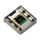
Small Form Factor: 2.0 mm × 2.0 mm × 0.65 mm
1
•
•
•
•
•
•
•
•
•
2 Applications
•
•
•
•
•
•
•
•
Intrusion and Door-Open Detection Systems
System Wake-Up Circuits
Medical and Scientific Instrumentation
Display Backlight Controls
Lighting Control Systems
Tablet and Notebook Computers
Thermostats and Home Automation Appliances
Outdoor Traffic and Street Lights
Use the OPT3002 in optical spectral systems that
require detection of a variety of wavelengths, such as
optically-based diagnostic systems. The interrupt pin
system can summarize the result of the measurement
with one digital pin. Power consumption is very low,
allowing the OPT3002 to be used as a low-power,
battery-operated, wake-up sensor when an enclosed
system is opened.
The OPT3002 is fully integrated and provides optical
power reading directly from the I2C- and SMBuscompatible, two-wire, serial interface. Measurements
are either continuous or single-shot. The OPT3002
fully-operational power consumption is as low as
0.8 µW at 0.8 SPS on a 1.8-V supply.
Device Information(1)
PART NUMBER
PACKAGE
OPT3002
USON (6)
BODY SIZE (NOM)
2.00 mm x 2.00 mm
(1) For all available packages, see the package option addendum
at the end of the datasheet.
Spectral Response
Block Diagram
VDD
1
OPT3002
0.9
Normalized Response
0.8
VDD
OPT3002
0.7
SCL
0.6
0.5
Light
ADC
I2C
SDA
Interface
INT
ADDR
0.4
0.3
0.2
GND
0.1
0
300
Copyright © 2016, Texas Instruments Incorporated
400
500
600
700
Wavelength (nm)
800
900
1000
D001
1
An IMPORTANT NOTICE at the end of this data sheet addresses availability, warranty, changes, use in safety-critical applications,
intellectual property matters and other important disclaimers. PRODUCTION DATA.
�OPT3002
SBOS745A – MAY 2016 – REVISED JUNE 2016
www.ti.com
Table of Contents
1
2
3
4
5
6
7
Features ..................................................................
Applications ...........................................................
Description .............................................................
Revision History.....................................................
Pin Configuration and Functions .........................
Specifications.........................................................
1
1
1
2
3
4
6.1
6.2
6.3
6.4
6.5
6.6
6.7
4
4
4
4
5
6
7
Absolute Maximum Ratings ......................................
ESD Ratings..............................................................
Recommended Operating Conditions.......................
Thermal Information ..................................................
Electrical Characteristics...........................................
Timing Requirements ................................................
Typical Characteristics ..............................................
Detailed Description ............................................ 10
7.1
7.2
7.3
7.4
7.5
Overview .................................................................
Functional Block Diagram ......................................
Feature Description.................................................
Device Functional Modes........................................
Programming...........................................................
10
10
11
13
16
7.6 Register Maps ......................................................... 19
8
Application and Implementation ........................ 26
8.1 Application Information............................................ 26
8.2 Do's and Don'ts ...................................................... 27
9 Power-Supply Recommendations...................... 27
10 Layout................................................................... 28
10.1 Layout Guidelines ................................................. 28
10.2 Layout Example .................................................... 28
11 Device and Documentation Support ................. 29
11.1
11.2
11.3
11.4
11.5
11.6
Documentation Support ........................................
Receiving Notification of Documentation Updates
Community Resources..........................................
Trademarks ...........................................................
Electrostatic Discharge Caution ............................
Glossary ................................................................
29
29
29
29
29
29
12 Mechanical, Packaging, and Orderable
Information ........................................................... 30
12.1 Soldering and Handling Recommendations.......... 30
12.2 DNP (S-PDSO-N6) Mechanical Drawings ............ 30
4 Revision History
NOTE: Page numbers for previous revisions may differ from page numbers in the current version.
Changes from Original (May 2016) to Revision A
•
2
Page
Released to production .......................................................................................................................................................... 1
Submit Documentation Feedback
Copyright © 2016, Texas Instruments Incorporated
Product Folder Links: OPT3002
�OPT3002
www.ti.com
SBOS745A – MAY 2016 – REVISED JUNE 2016
5 Pin Configuration and Functions
DNP Package
6-Pin USON
Top View
VDD
1
6
SDA
ADDR
2
5
INT
GND
3
4
SCL
Not to scale
Pin Functions
PIN
NO.
NAME
DESCRIPTION
I/O
1
VDD
Power
2
ADDR
Digital input
3
GND
Power
4
SCL
Digital input
5
INT
Digital output
6
SDA
Digital input/output
Device power. Connect to a 1.6-V to 3.6-V supply.
Address pin. This pin sets the LSBs of the I2C address.
Ground
I2C clock. Connect with a 10-kΩ resistor to a 1.6-V to 5.5-V supply.
Interrupt output open-drain. Connect with a 10-kΩ resistor to a 1.6-V to 5.5-V supply.
I2C data. Connect with a 10-kΩ resistor to a 1.6-V to 5.5-V supply.
Submit Documentation Feedback
Copyright © 2016, Texas Instruments Incorporated
Product Folder Links: OPT3002
3
�OPT3002
SBOS745A – MAY 2016 – REVISED JUNE 2016
www.ti.com
6 Specifications
6.1 Absolute Maximum Ratings (1)
Voltage
MIN
MAX
VDD to GND
–0.5
6
SDA, SCL, INT, and ADDR to GND
–0.5
6
Current into any pin
(1)
(2)
V
10
Junction, TJ
Temperature
UNIT
mA
150
Storage, Tstg
°C
150 (2)
–65
Stresses beyond those listed under Absolute Maximum Ratings may cause permanent damage to the device. These are stress ratings
only, which do not imply functional operation of the device at these or any other conditions beyond those indicated under Recommended
Operating Conditions. Exposure to absolute-maximum-rated conditions for extended periods may affect device reliability.
Long exposure to temperatures higher than 105°C can cause package discoloration, spectral distortion, and measurement inaccuracy.
6.2 ESD Ratings
VALUE
V(ESD)
(1)
(2)
Electrostatic discharge
Human-body model (HBM), per ANSI/ESDA/JEDEC JS-001 (1)
±2000
Charged-device model (CDM), per JEDEC specification JESD22-C101 (2)
±500
UNIT
V
JEDEC document JEP155 states that 500-V HBM allows safe manufacturing with a standard ESD control process.
JEDEC document JEP157 states that 250-V CDM allows safe manufacturing with a standard ESD control process.
6.3 Recommended Operating Conditions
MIN
NOM
MAX
UNIT
Operating power-supply voltage
1.6
3.6
V
Operating temperature
–40
85
°C
6.4 Thermal Information
OPT3002
THERMAL METRIC (1)
DNP (USON)
UNIT
6 PINS
RθJA
Junction-to-ambient thermal resistance
71.2
°C/W
RθJC(top)
Junction-to-case (top) thermal resistance
45.7
°C/W
RθJB
Junction-to-board thermal resistance
42.2
°C/W
ψJT
Junction-to-top characterization parameter
2.4
°C/W
ψJB
Junction-to-board characterization parameter
42.8
°C/W
RθJC(bot)
Junction-to-case (bottom) thermal resistance
17.0
°C/W
(1)
4
For more information about traditional and new thermal metrics, see the Semiconductor and IC Package Thermal Metrics application
report.
Submit Documentation Feedback
Copyright © 2016, Texas Instruments Incorporated
Product Folder Links: OPT3002
�OPT3002
www.ti.com
SBOS745A – MAY 2016 – REVISED JUNE 2016
6.5 Electrical Characteristics
at TA = 25°C, VDD = 3.3 V, 800-ms conversion time (CT = 1) (1), automatic full-scale range (RN[3:0] = 1100b (1)), 505-nm LED
stimulus, and normal-angle incidence of light (unless otherwise specified)
PARAMETER
TEST CONDITIONS
MIN
TYP
MAX
UNIT
OPTICAL
Peak irradiance spectral responsivity
Resolution (LSB) at 505 nm
Lowest full-scale range (FSR), RN[3:0] =
0000b (1)
Full-scale illuminance at 505 nm
Measurement output result
505-nm LED stimulus, FSR setting = 628,992
(nW/cm2), 153.6 (nW/cm2) per ADC code
(RN[3:0] = 0111) (1)
2 klux white LED stimulus, FSR setting =
628,992 (nW/cm2), 153.6 (nW/cm2) per ADC
code (RN[3:0] = 0111) (1) (3)
nm
1.2
nW/cm2 (2)
10.064
mW/cm2 (2)
384,000
nW/cm2 (2)
2500
2250
Relative accuracy between gain
ranges (4)
2500
ADC codes
2750
ADC codes
3
ADC codes
0.2%
Infrared response (850 nm) relative to
response at 505 nm (3)
20%
2
Linearity
505
2%
Input illuminance > 5000 nW/cm
Input illuminance < 5000 nW/cm2
5%
2
PSRR
Dark condition, ADC output
Lowest FSR, RN[3:0] = 0000b, 4914 (nW/cm ),
1.2 (nW/cm2) per ADC code
Half-power angle
50% of full-power reading
60
Degrees
Power-supply rejection ratio
VDD at 3.6 V and 1.6 V
0.1
%/V (5)
0
POWER SUPPLY
I2C pullup resistor operating range
VI²C
I2C pullup resistor, VDD ≤ VI²C
Dark
IQ
Quiescent current
Full-scale
range
POR
Power-on-reset threshold
1.6
5.5
Active, VDD = 3.6 V
1.8
2.5
Shutdown (M[1:0] = 00) (1),
VDD = 3.6 V
0.3
0.47
Active, VDD = 3.6 V
3.7
Shutdown,
(M[1:0] = 00) (1)
0.4
TA = 25°C
V
µA
0.8
V
DIGITAL
I/O pin capacitance
Total integration time (6)
3
pF
(CT = 1) (1), 800-ms mode, fixed FSR
720
800
880
(CT = 0) (1), 100-ms mode, fixed FSR
90
100
110
ms
VIL
Low-level input voltage
(SDA, SCL, and ADDR)
0
0.3 × VDD
V
VIH
High-level input voltage
(SDA, SCL, and ADDR)
0.7 × VDD
5.5
V
IIL
Low-level input current
(SDA, SCL, and ADDR)
0.25 (7)
µA
VOL
Low-level output voltage
(SDA and INT)
IOL = 3 mA
0.32
V
IZH
Output logic high, high-Z leakage
current (SDA, INT)
At VDD pin
0.25 (7)
µA
(1)
(2)
(3)
(4)
(5)
(6)
(7)
0.01
0.01
Refers to a control field within the configuration register.
All nW/cm2 units assume a 505-nm stimulus. To scale the LSB size, full-scale, and results at other wavelengths, see the Compensation
for the Spectral Response section.
Tested with the white LED calibrated to 2 klux and an 850-nm LED.
Characterized by measuring fixed near-full-scale light levels on the higher adjacent full-scale range setting.
PSRR is the percent change of the measured optical power output from its current value, divided by the change in power-supply
voltage, as characterized by results from the 3.6-V and 1.6-V power supplies.
The conversion time, from start of conversion until data are ready to be read, is the integration time plus 3 ms.
The specified leakage current is dominated by the production test equipment limitations. Typical values are much smaller.
Submit Documentation Feedback
Copyright © 2016, Texas Instruments Incorporated
Product Folder Links: OPT3002
5
�OPT3002
SBOS745A – MAY 2016 – REVISED JUNE 2016
www.ti.com
6.6 Timing Requirements (1)
MIN
TYP
MAX
UNIT
0.4
MHz
I2C FAST MODE
fSCL
SCL operating frequency
0.01
tBUF
Bus free time between stop and start
1300
ns
tHDSTA
Hold time after repeated start
600
ns
tSUSTA
Setup time for repeated start
600
ns
tSUSTO
Setup time for stop
600
ns
tHDDAT
Data hold time
20
tSUDAT
Data setup time
100
ns
tLOW
SCL clock low period
1300
ns
tHIGH
SCL clock high period
600
tRC and tFC
Clock rise and fall time
300
ns
tRD and tFD
Data rise and fall time
300
ns
tTIMEO
Bus timeout period. If the SCL line is held low for this duration of time, then the
bus state machine is reset.
900
ns
ns
28
ms
2
I C HIGH-SPEED MODE
fSCL
SCL operating frequency
0.01
tBUF
Bus free time between stop and start
160
ns
tHDSTA
Hold time after repeated start
160
ns
tSUSTA
Setup time for repeated start
160
ns
tSUSTO
Setup time for stop
160
tHDDAT
Data hold time
20
tSUDAT
Data setup time
20
ns
tLOW
SCL clock low period
240
ns
tHIGH
SCL clock high period
60
tRC and tFC
Clock rise and fall time
40
ns
tRD and tFD
Data rise and fall time
80
ns
tTIMEO
Bus timeout period. If the SCL line is held low for this duration of time, then the
bus state machine is reset.
(1)
2.6
MHz
ns
140
ns
ns
28
ms
All timing parameters are referenced to low and high voltage thresholds of 30% and 70%, respectively, of the final settled value.
1/fSCL
tRC
tFC
70%
30%
SCL
tLOW
tHDDAT tHIGH
tSUDAT
tSUSTA
tHDSTA
tSUSTO
70%
30%
SDA
tBUF
Stop
Start
tRD
tFD
Start
Stop
Figure 1. I2C Detailed Timing Diagram
6
Submit Documentation Feedback
Copyright © 2016, Texas Instruments Incorporated
Product Folder Links: OPT3002
�OPT3002
www.ti.com
SBOS745A – MAY 2016 – REVISED JUNE 2016
6.7 Typical Characteristics
at TA = 25°C, VDD = 3.3 V, 800-ms conversion time (CT = 1), automatic full-scale range (RN[3:0] = 1100b), white LED, and
normal-angle incidence of light (unless otherwise specified)
1
1.020
OPT3002
0.9
1.010
0.7
Relative Response
Normalized Response
0.8
0.6
0.5
0.4
0.3
1.000
1.000
1.001
1.002
1.001
1.002
0.997
0.997
39312
78624 157248 314496
0.990
0.2
0.1
0
300
400
500
600
700
Wavelength (nm)
800
900
0.980
1000
4914
9828
19656
Full-Scale Range ( nW/cm2)
D001
D006
Input illuminance = 3960 nW/cm2,
normalized to response of 4914 nW/cm2 full-scale
Figure 2. Spectral Response vs Wavelength
Figure 3. Full-Scale-Range Matching (Lowest 7 Ranges)
10
Dark Output Response (nW/cm2)
1.020
Relative Response
1.010
1.000
1.000
1.002
1.003
1.004
1.002
1.000
0.990
9
8
7
6
5
4
3
2
1
0
-40
0.980
314496
628992 1257984 2515968 5031936 10063872
Full-Scale Range (nW/cm2)
-20
0
D007
Input illuminance = 298,800 nW/cm ,
normalized to response of 314,496 nW/cm2 full-scale
80
100
D0016
Figure 5. Dark Response vs Temperature
Figure 4. Full-Scale-Range Matching (Highest 6 Ranges)
1.2
1000
400nm
550nm
700nm
1.1
Conversion Time (ms)
Normalized Response
60
Average of 30 devices
2
1.15
20
40
Temperature (qC)
1.05
1
0.95
0.9
900
800
700
0.85
0.8
-40 -30 -20 -10
0
10 20 30 40 50 60 70 80 90
Temperature [°C]
D008
Figure 6. Normalized Response vs Temperature
600
1.6
2
2.4
2.8
Power Supply (V)
3.2
3.6
D017
Figure 7. Conversion Time vs Power Supply
Submit Documentation Feedback
Copyright © 2016, Texas Instruments Incorporated
Product Folder Links: OPT3002
7
�OPT3002
SBOS745A – MAY 2016 – REVISED JUNE 2016
www.ti.com
Typical Characteristics (continued)
at TA = 25°C, VDD = 3.3 V, 800-ms conversion time (CT = 1), automatic full-scale range (RN[3:0] = 1100b), white LED, and
normal-angle incidence of light (unless otherwise specified)
1
OPT3002 Normalized Response
1.002
Normalized Response
1.001
1
0.999
0.9
0.8
0.7
0.6
0.5
0.4
0.3
0.2
0.1
0.998
1.6
2
2.4
2.8
Power Supply (V)
3.2
0
-80
3.6
0.5
3.5
0.45
3
2.5
2
60
80
D010
0.4
0.35
0.3
0.2
1
10000
100000
1000000
Input Illuminance (nW/cm 2)
0
1E+7
2000000 4000000 6000000 8000000
Input Illuminance (nW/cm 2)
D011
M[1:0] = 10b, illuminance derived from white LED
1E+7
1.2E+7
D011
D012
M[1:0] = 00b, illuminance derived from white LED
Figure 10. Supply Current in Active State vs
Input Illuminance
Figure 11. Supply Current in Shutdown State vs
Input Illuminance
3.5
1.6
Shutdown Supply Current (PA)
Vdd = 3.3V
Vdd = 1.6V
3
Supply Current (PA)
-20
0
20
40
Incidence Angle (Degrees)
0.25
1.5
2.5
2
1.5
-20
0
20
40
Temperature (qC)
60
80
100
Vdd = 3.3V
Vdd = 1.6V
1.4
1.2
1
0.8
0.6
0.4
0.2
-40
-20
D013
0
20
40
Temperature (qC)
60
80
100
D014
M[1:0] = 00b, input illuminance = 0 nW/cm2
M[1:0] = 10b
Figure 12. Supply Current in Active State vs Temperature
8
-40
Figure 9. Normalized Response vs Incidence Angle
4
Supply Current (PA)
Supply Current (PA)
Figure 8. Normalized Response vs Power-Supply Voltage
1
-40
-60
D009
Figure 13. Supply Current in Shutdown State vs
Temperature
Submit Documentation Feedback
Copyright © 2016, Texas Instruments Incorporated
Product Folder Links: OPT3002
�OPT3002
www.ti.com
SBOS745A – MAY 2016 – REVISED JUNE 2016
Typical Characteristics (continued)
at TA = 25°C, VDD = 3.3 V, 800-ms conversion time (CT = 1), automatic full-scale range (RN[3:0] = 1100b), white LED, and
normal-angle incidence of light (unless otherwise specified)
100
Shutdown Current (PA)
Vdd = 3.3V
Vdd = 1.6V
10
1
0.1
0.01
0.1
1
10
100
1000
Continuous I2C Frequency (KHz)
10000
D015
SCL = SDA, continuously toggled at I2C frequency
Note: A typical application runs at a lower duty cycle and thus consumes a lower current.
Figure 14. Supply Current in Shutdown State vs Continuous I2C Frequency
Submit Documentation Feedback
Copyright © 2016, Texas Instruments Incorporated
Product Folder Links: OPT3002
9
�OPT3002
SBOS745A – MAY 2016 – REVISED JUNE 2016
www.ti.com
7 Detailed Description
7.1 Overview
The OPT3002 measures the light that illuminates the device within the device spectral range of 300 nm to
1000 nm.
The OPT3002 is fully self-contained to measure the ambient light and report the result digitally over the I2C bus.
The result can also be used to alert a system and interrupt a processor with the INT pin. The result can also be
summarized with a programmable window comparison and communicated with the INT pin.
The OPT3002 can be configured into an automatic full-scale, range-setting mode that always selects the optimal
full-scale range setting for the lighting conditions. This mode automatically selects the optimal full-scale range for
the given lighting condition, thus eliminating the requirement of programming many measurement and
readjustment cycles of the full-scale range. The device can operate continuously or in single-shot measurement
modes.
The device integrates its result over either 100 ms or 800 ms, so the effects of 50-Hz and 60-Hz noise sources
from typical light bulbs are nominally reduced to a minimum.
The device starts up in a low-power shutdown state, such that the OPT3002 only consumes active-operation
power after being programmed into an active state.
7.2 Functional Block Diagram
VDD
VDD
OPT3002
SCL
Light
ADC
I2C
SDA
Interface
INT
ADDR
GND
Copyright © 2016, Texas Instruments Incorporated
10
Submit Documentation Feedback
Copyright © 2016, Texas Instruments Incorporated
Product Folder Links: OPT3002
�OPT3002
www.ti.com
SBOS745A – MAY 2016 – REVISED JUNE 2016
7.3 Feature Description
7.3.1 Automatic Full-Scale Range Setting
The OPT3002 has an automatic full-scale range setting feature that eliminates the need to predict and set the
optimal range for the device. In this mode, the OPT3002 automatically selects the optimal full-scale range for the
given lighting condition. The OPT3002 has a high degree of result matching between the full-scale range
settings. This matching eliminates the problem of varying results or the need for range-specific, user-calibrated
gain factors when different full-scale ranges are chosen. For further details, see the Automatic Full-Scale Setting
Mode section.
7.3.2 Interrupt Operation, INT Pin, and Interrupt Reporting Mechanisms
The device has an interrupt reporting system that allows the processor connected to the I2C bus to go to sleep,
or otherwise ignore the device results, until a user-defined event occurs that requires possible action.
Alternatively, this same mechanism can also be used with any system that can take advantage of a single digital
signal that indicates whether the light is above or below the levels of interest.
The interrupt event conditions are controlled by the high-limit and low-limit registers, as well as the configuration
register latch and fault count fields. The results of comparing the result register with the high-limit register and
low-limit register are referred to as fault events. The fault count field (configuration register, bits FC[1:0]) dictates
how many consecutive same-result fault events are required to trigger an interrupt event and subsequently
change the state of the interrupt reporting mechanisms (that is, the INT pin, the flag high field, and the flag low
field). The latch field allows a choice between a latched window-style comparison and a transparent hysteresisstyle comparison.
The INT pin has an open-drain output that requires the use of a pullup resistor. This open-drain output allows
multiple devices with open-drain INT pins to be connected to the same line, thus creating a logical NOR or AND
function between the devices. The polarity of the INT pin can be controlled with the polarity of the interrupt field
in the configuration register. When the POL field is set to 0, the pin operates in an active low behavior that pulls
the pin low when the INT pin becomes active. When the POL field is set to 1, the pin operates in an active high
behavior and becomes high impedance, thus allowing the pin to go high when the INT pin becomes active.
Additional details of the interrupt reporting registers are described in the Interrupt Reporting Mechanism Modes
and Internal Registers sections.
Submit Documentation Feedback
Copyright © 2016, Texas Instruments Incorporated
Product Folder Links: OPT3002
11
�OPT3002
SBOS745A – MAY 2016 – REVISED JUNE 2016
www.ti.com
Feature Description (continued)
7.3.3 I2C Bus Overview
The OPT3002 offers compatibility with both I2C and SMBus interfaces. The I2C and SMBus protocols are
essentially compatible with one another. The I2C interface is used throughout this document as the primary
example with the SMBus protocol specified only when a difference between the two protocols is discussed.
The OPT3002 is connected to the bus with two pins: an SCL clock input pin and an SDA open-drain bidirectional
data pin. The bus must be controlled by a master device that generates the serial clock (SCL), controls the bus
access, and generates start and stop conditions. To address a specific device, the master initiates a start
condition by pulling the data signal line (SDA) from a high logic level to a low logic level when SCL is high. All
slaves on the bus shift in the slave address byte on the SCL rising edge, with the last bit indicating whether a
read or write operation is intended. During the ninth clock pulse, the slave being addressed responds to the
master by generating an acknowledge bit by pulling SDA low.
Data transfer is then initiated and eight bits of data are sent, followed by an acknowledge bit. During data
transfer, SDA must remain stable when SCL is high. Any change in SDA when SCL is high is interpreted as a
start or stop condition. When all data are transferred, the master generates a stop condition, as indicated by
pulling SDA from low to high when SCL is high. The OPT3002 includes a 28-ms timeout on the I2C interface to
prevent locking up the bus. If the SCL line is held low for this duration of time, then the bus state machine is
reset.
7.3.3.1 Serial Bus Address
To communicate with the OPT3002, the master must first initiate an I2C start command. Then, the master must
address slave devices via a slave address byte. The slave address byte consists of seven address bits and a
direction bit that indicates whether the action is to be a read or write operation.
Four I2C addresses are possible by connecting the ADDR pin to one of four pins: GND, VDD, SDA, or SCL.
Table 1 summarizes the possible addresses with the corresponding ADDR pin configuration. The state of the
ADDR pin is sampled on every bus communication and must be driven or connected to the desired level before
any activity on the interface occurs.
Table 1. Possible I2C Addresses with the Corresponding ADDR Configuration
DEVICE I2C ADDRESS
ADDR PIN
1000100
GND
1000101
VDD
1000110
SDA
1000111
SCL
7.3.3.2 Serial Interface
The OPT3002 operates as a slave device on both the I2C bus and SMBus. Connections to the bus are made via
the SCL clock input line and the SDA open-drain I/O line. The OPT3002 supports the transmission protocol for
standard mode (up to 100 kHz), fast mode (up to 400 kHz), and high-speed mode (up to 2.6 MHz). All data bytes
are transmitted most-significant bits first.
The SDA and SCL pins feature integrated spike-suppression filters and Schmitt triggers to minimize the effects of
input spikes and bus noise. See the Electrical Interface section for further details of the I2C bus noise immunity.
12
Submit Documentation Feedback
Copyright © 2016, Texas Instruments Incorporated
Product Folder Links: OPT3002
�OPT3002
www.ti.com
SBOS745A – MAY 2016 – REVISED JUNE 2016
7.4 Device Functional Modes
7.4.1 Automatic Full-Scale Setting Mode
The OPT3002 has an automatic full-scale-range setting mode that eliminates the need for a user to predict and
set the optimal range for the device. This mode is entered when the configuration register range number field
(RN[3:0]) is set to 1100b.
The first measurement that the device takes in auto-range mode is a 10-ms range assessment measurement.
The device then determines the appropriate full-scale range to take its first full measurement.
For subsequent measurements, the full-scale range is set by the result of the previous measurement. If a
measurement is towards the low side of full-scale, then the full-scale range is decreased by one or two settings
for the next measurement. If a measurement is towards the upper side of full-scale, then the full-scale range is
increased by one setting for the next measurement.
If the measurement exceeds the full-scale range, resulting from a fast-increasing optical transient event, then the
current measurement is aborted. This invalid measurement is not reported. A 10-ms measurement is taken to
assess and properly reset the full-scale range. Then, a new measurement is taken with this proper full-scale
range. Therefore, during a fast-increasing optical transient in this mode, a measurement can possibly take longer
to complete and report than indicated by the configuration register conversion time field (CT).
7.4.2 Interrupt Reporting Mechanism Modes
There are two major types of interrupt reporting mechanism modes: latched window-style comparison mode and
transparent hysteresis-style comparison mode. The configuration register latch field (L) (see the configuration
register, bit 4) controls which of these two modes is used. An end-of-conversion mode is also associated with
each major mode type. The end-of-conversion mode is active when the two most significant bits of the threshold
low register are set to 11b. The mechanisms report via the flag high and flag low fields, the conversion ready
field, and the INT pin.
7.4.2.1 Latched Window-Style Comparison Mode
The latched window-style comparison mode is typically selected when using the OPT3002 to interrupt an
external processor. In this mode, a fault is recognized when the input signal is above the high-limit register or
below the low-limit register. When the consecutive fault events trigger the interrupt reporting mechanisms, these
mechanisms are latched, thus reporting whether the fault is the result of a high or low comparison. These
mechanisms remain latched until the configuration register is read, which clears the INT pin and flag high and
flag low fields. The SMBus alert response protocol, described in detail in the SMBus Alert Response section,
clears the pin but does not clear the flag high and flag low fields. The behavior of this mode, along with the
conversion ready flag, is summarized in Table 2. Note that Table 2 does not apply when the two threshold low
register MSBs (see the Transparent Hysteresis-Style Comparison Mode section for clarification on the MSBs) are
set to 11b.
Submit Documentation Feedback
Copyright © 2016, Texas Instruments Incorporated
Product Folder Links: OPT3002
13
�OPT3002
SBOS745A – MAY 2016 – REVISED JUNE 2016
www.ti.com
Device Functional Modes (continued)
Table 2. Latched Window-Style Comparison Mode: Flag Setting and Clearing Summary (1) (2)
FLAG HIGH
FIELD
FLAG LOW
FIELD
INT PIN (3)
CONVERSION
READY FIELD
The result register is above the high-limit register for fault count times;
see the result register and the high-limit register for further details.
1
X
Active
1
The result register is below the low-limit register for fault count times;
see the result register and the low-limit register for further details.
X
1
Active
1
The conversion is complete with fault count criterion not met
X
X
X
1
OPERATION
Configuration register read
(4)
0
0
Inactive
0
Configuration register write, M[1:0] = 00b (shutdown)
X
X
X
X
Configuration register write, M[1:0] > 00b (not shutdown)
X
X
X
0
SMBus alert response protocol
X
X
Inactive
X
(1)
(2)
(3)
(4)
X = no change from the previous state.
The high-limit register is assumed to be greater than the low-limit register. If this assumption is incorrect, the flag high field and flag low
field can take on different behaviors.
The INT pin depends on the setting of the polarity field (POL). The INT pin is low when the pin state is active and POL = 0 (active low)
or when the pin state is inactive and POL = 1 (active high).
Immediately after the configuration register is read, the device automatically resets the conversion ready field to its 0 state. Thus, if two
configuration register reads are performed immediately after a conversion completion, the first reads 1 and the second reads 0.
7.4.2.2 Transparent Hysteresis-Style Comparison Mode
The transparent hysteresis-style comparison mode is typically used when a single digital signal is desired that
indicates whether the input light is higher than or lower than a light level of interest. If the result register is higher
than the high-limit register for a consecutive number of events set by the fault count field, then the INT line is set
to active, the flag high field is set to 1, and the flag low field is set to 0. If the result register is lower than the lowlimit register for a consecutive number of events set by the fault count field, then the INT line is set to inactive,
the flag low field is set to 1, and the flag high field is set to 0. The INT pin and flag high and flag low fields do not
change state with configuration reads and writes. The INT pin and flag fields continually report the appropriate
comparison of the light to the low-limit and high-limit registers. The device does not respond to the SMBus alert
response protocol when in either of the two transparent comparison modes (configuration register, latch field =
0). The behavior of this mode, along with the conversion ready is summarized in Table 3. Note that Table 3 does
not apply when the two threshold low register MSBs (LE[3:2] from Table 11) are set to 11.
Table 3. Transparent Hysteresis-Style Comparison Mode: Flag Setting and Clearing Summary (1) (2)
FLAG HIGH
FIELD
FLAG LOW
FIELD
INT PIN (3)
CONVERSION
READY FIELD
The result register is above the high-limit register for fault count times;
see the result register and the high-limit register for further details.
1
0
Active
1
The result register is below the low-limit register for fault count times;
see the result register and the low-limit register for further details.
0
1
Inactive
1
The conversion is complete with fault count criterion not met
X
X
X
1
OPERATION
Configuration register read
(4)
X
X
X
0
Configuration register write, M[1:0] = 00b (shutdown)
X
X
X
X
Configuration register write, M[1:0] > 00b (not shutdown)
X
X
X
0
SMBus alert response protocol
X
X
X
X
(1)
(2)
(3)
(4)
14
X = no change from the previous state.
The high-limit register is assumed to be greater than the low-limit register. If this assumption is incorrect, the flag high field and flag low
field can take on different behaviors.
The INT pin depends on the setting of the polarity field (POL). The INT pin is low when the pin state is active and POL = 0 (active low)
or when the pin state is inactive and POL = 1 (active high).
Immediately after the configuration register is read, the device automatically resets the conversion ready field to its 0 state. Thus, if two
configuration register reads are performed immediately after a conversion completion, the first reads 1 and the second reads 0.
Submit Documentation Feedback
Copyright © 2016, Texas Instruments Incorporated
Product Folder Links: OPT3002
�OPT3002
www.ti.com
SBOS745A – MAY 2016 – REVISED JUNE 2016
7.4.2.3 End-of-Conversion Mode
An end-of-conversion indicator mode can be used when every measurement is desired to be read by the
processor, prompted by the INT pin going active on every measurement completion. This mode is entered by
setting the most significant two bits of the low-limit register (LE[3:2] from the low-limit register) to 11b. This endof-conversion mode is typically used in conjunction with the latched window-style comparison mode. The INT pin
becomes inactive when the configuration register is read or the configuration register is written with a nonshutdown parameter or in response to an SMBus alert response. Table 4 summarizes the interrupt reporting
mechanisms as a result of various operations.
Table 4. End-of-Conversion Mode When in Latched Window-Style Comparison Mode:
Flag Setting and Clearing Summary (1)
FLAG HIGH
FIELD
FLAG LOW
FIELD
INT PIN (2)
CONVERSION
READY FIELD
The result register is above the high-limit register for fault count times;
see the result register and the high-limit register for further details.
1
X
Active
1
The result register is below the low-limit register for fault count times;
see the result register and the low-limit register for further details.
X
1
Active
1
The conversion is complete with fault count criterion not met
X
X
Active
1
OPERATION
Configuration register read
(3)
0
0
Inactive
0
Configuration register write, M[1:0] = 00b (shutdown)
X
X
X
X
Configuration register write, M[1:0] > 00b (not shutdown)
X
X
X
0
SMBus alert response protocol
X
X
Inactive
X
(1)
(2)
(3)
X = no change from the previous state.
The INT pin depends on the setting of the polarity field (POL). The INT pin is low when the pin state is active and POL = 0 (active low)
or when the pin state is inactive and POL = 1 (active high).
Immediately after the configuration register is read, the device automatically resets the conversion ready field to its 0 state. Thus, if two
configuration register reads are performed immediately after a conversion completion, the first reads 1 and the second reads 0.
Note that when transitioning from end-of-conversion mode to the standard comparison modes (that is,
programming LE[3:2] from 11b to 00b) when the configuration register latch field (L) is 1, a subsequent write to
the configuration register latch field (L) to 0 is necessary in order to properly clear the INT pin. The latch field can
then be set back to 1 if desired.
7.4.2.4 End-of-Conversion and Transparent Hysteresis-Style Comparison Mode
The combination of end-of-conversion mode and transparent hysteresis-style comparison mode can also be
programmed simultaneously. The behavior of this combination is shown in Table 5.
Table 5. End-Of-Conversion Mode When in Transparent Hysteresis-Style Comparison Mode:
Flag Setting and Clearing Summary (1)
FLAG HIGH
FIELD
FLAG LOW
FIELD
INT PIN (2)
CONVERSION
READY FIELD
The result register is above the high-limit register for fault count times;
see the result register and the high-limit register for further details.
1
0
Active
1
The result register is below the low-limit register for fault count times;
see the result register and the low-limit register for further details.
0
1
Active
1
The conversion is complete with fault count criterion not met
X
X
Active
1
Configuration register read (3)
X
X
Inactive
0
Configuration register write, M[1:0] = 00b (shutdown)
X
X
X
X
Configuration register write, M[1:0] > 00b (not shutdown)
X
X
Inactive
0
SMBus alert response protocol
X
X
X
X
OPERATION
(1)
(2)
(3)
X = no change from the previous state.
The INT pin depends on the setting of the polarity field (POL). The INT pin is low when the pin state is active and POL = 0 (active low)
or when the pin state is inactive and POL = 1 (active high).
Immediately after the configuration register is read, the device automatically resets the conversion ready field to its 0 state. Thus, if two
configuration register reads are performed immediately after a conversion completion, the first reads 1 and the second reads 0.
Submit Documentation Feedback
Copyright © 2016, Texas Instruments Incorporated
Product Folder Links: OPT3002
15
�OPT3002
SBOS745A – MAY 2016 – REVISED JUNE 2016
www.ti.com
7.5 Programming
The OPT3002 supports the transmission protocol for standard mode (up to 100 kHz), fast mode (up to 400 kHz),
and high-speed mode (up to 2.6 MHz). Fast and standard modes are described as the default protocol, referred
to as F/S. High-speed mode is described in the High-Speed I2C Mode section.
7.5.1 Writing and Reading
Accessing a specific register on the OPT3002 is accomplished by writing the appropriate register address during
the I2C transaction sequence. See Table 6 for a complete list of registers and the corresponding register
addresses. The value for the register address (as shown in Figure 15) is the first byte transferred after the slave
address byte with the R/W bit low.
1
9
1
9
SCL
SDA
1
0
0
0
Start by
Master
1
A1
A0
R/W
RA
7
RA
6
RA
5
RA
4
RA
3
RA
2
RA
1
ACK by
OPT3002
Frame 1: Two-Wire Slave Address Byte (1)
RA
0
ACK by
OPT3002
Stop by
Master
(optional)
Frame 2: Register Address Byte
(1) The value of the slave address byte is determined by the ADDR pin setting; see Table 1.
Figure 15. Setting the I2C Register Address Timing Diagram
Writing to a register begins with the first byte transmitted by the master. This byte is the slave address with the
R/W bit low. The OPT3002 then acknowledges receipt of a valid address. The next byte transmitted by the
master is the address of the register that data are to be written to. The next two bytes are written to the register
addressed by the register address. The OPT3002 acknowledges receipt of each data byte. The master can
terminate the data transfer by generating a start or stop condition.
When reading from the OPT3002, the last value stored in the register address by a write operation determines
which register is read during a read operation. To change the register address for a read operation, a new partial
I2C write transaction must be initiated. This partial write is accomplished by issuing a slave address byte with the
R/W bit low, followed by the register address byte and a stop command. The master then generates a start
condition and sends the slave address byte with the R/W bit high to initiate the read command. The next byte is
transmitted by the slave and is the most significant byte of the register indicated by the register address. This
byte is followed by an acknowledge from the master; then the slave transmits the least significant byte. The
master acknowledges receipt of the data byte. The master can terminate the data transfer by generating a notacknowledge after receiving any data byte, or by generating a start or stop condition. If repeated reads from the
same register are desired, continually sending the register address bytes is not necessary; the OPT3002 retains
the register address until that number is changed by the next write operation.
16
Submit Documentation Feedback
Copyright © 2016, Texas Instruments Incorporated
Product Folder Links: OPT3002
�OPT3002
www.ti.com
SBOS745A – MAY 2016 – REVISED JUNE 2016
Programming (continued)
Figure 16 and Figure 17 show the write and read operation timing diagrams, respectively. Note that register
bytes are sent most significant byte first, followed by the least significant byte.
1
9
9
1
1
9
1
9
SCL
SDA
1
0
0
0
1
A1
A0
Start by
Master
RA
7
R/W
RA
6
RA
5
RA
4
RA
3
RA
2
RA
1
RA
0
ACK by
OPT3002
Frame 1 Two-Wire Slave Address Byte (1)
D15 D14 D13 D12 D11 D10 D9
Frame 2 Register Address Byte
D8
D7
D6
D5
D4
D3
D2
D1
D0
ACK by
OPT3002
ACK by
OPT3002
ACK by
OPT3002
Frame 3 Data MSByte
Stop by
Master
Frame 4 Data LSByte
(1) The value of the slave address byte is determined by the setting of the ADDR pin; see Table 1.
Figure 16. I2C Write Example Timing Diagram
1
9
1
9
1
9
SCL
SDA
1
0
0
0
1
A1
A0 R/W
Start by
Master
D15 D14 D13 D12 D11 D10 D9
ACK by
OPT3002
Frame 1 Two-Wire Slave Address Byte (1)
From
OPT3002
D8
D7
D6
D5
ACK by
Master
Frame 2 Data MSByte
D4
D3
D2
D1
From
OPT3002
D0
No ACK Stop by
by
Master
Master(2)
Frame 3 Data LSByte
(1) The value of the slave address byte is determined by the ADDR pin setting; see Table 1.
(2) An ACK by the master can also be sent.
Figure 17. I2C Read Example Timing Diagram
7.5.1.1 High-Speed I2C Mode
When the bus is idle, both the SDA and SCL lines are pulled high by the pullup resistors or the active pullup
devices. The master generates a start condition followed by a valid serial byte containing the high-speed (HS)
master code 0000 1XXXb. This transmission is made in either standard mode or fast mode (up to 400 kHz). The
OPT3002 does not acknowledge the HS master code but does recognize the code and switches its internal filters
to support a 2.6-MHz operation.
The master then generates a repeated start condition (a repeated start condition has the same timing as the start
condition). After this repeated start condition, the protocol is the same as F/S mode, except that transmission
speeds up to 2.6 MHz are allowed. Instead of using a stop condition, use repeated start conditions to secure the
bus in HS mode. A stop condition ends the HS mode and switches all internal filters of the OPT3002 to support
the F/S mode.
7.5.1.2 General-Call Reset Command
The I2C general-call reset allows the host controller in one command to reset all devices on the bus that respond
to the general-call reset command. The general call is initiated by writing to the I2C address 0 (0000 0000b). The
reset command is initiated when the subsequent second address byte is 06h (0000 0110b). With this transaction,
the device issues an acknowledge bit and sets all of its registers to the power-on-reset default condition.
Submit Documentation Feedback
Copyright © 2016, Texas Instruments Incorporated
Product Folder Links: OPT3002
17
�OPT3002
SBOS745A – MAY 2016 – REVISED JUNE 2016
www.ti.com
Programming (continued)
7.5.1.3 SMBus Alert Response
The SMBus alert response provides a quick identification for which device issued the interrupt. Without this alert
response capability, the processor does not know which device pulled the interrupt line when there are multiple
slave devices connected.
The OPT3002 is designed to respond to the SMBus alert response address, when in the latched window-style
comparison mode (configuration register, latch field = 1). The OPT3002 does not respond to the SMBus alert
response when in transparent mode (configuration register, latch field = 0).
The response behavior of the OPT3002 to the SMBus alert response is shown in Figure 18. When the interrupt
line to the processor is pulled to active, the master can broadcast the alert response slave address (0001
1001b). Following this alert response, any slave devices that generated an alert identify themselves by
acknowledging the alert response and sending their respective I2C address on the bus. The alert response can
activate several different slave devices simultaneously. If more than one slave attempts to respond, bus
arbitration rules apply. The device with the lowest address wins the arbitration. If the OPT3002 loses the
arbitration, then the device does not acknowledge the I2C transaction and its INT pin remains in an active state,
prompting the I2C master processor to issue a subsequent SMBus alert response. When the OPT3002 wins the
arbitration, the device acknowledges the transaction and sets its INT pin to inactive. The master can issue that
same command again, as many times as necessary to clear the INT pin. See the Interrupt Reporting Mechanism
Modes section for additional details of how the flags and INT pin are controlled. The master can obtain
information about the source of the OPT3002 interrupt from the address broadcast in the above process. The
flag high field (configuration register, bit 6) is sent as the final LSB of the address to provide the master additional
information about the cause of the OPT3002 interrupt. If the master requires additional information, then the
result register or the configuration register can be queried. The flag high and flag low fields are not cleared upon
an SMBus alert response.
INT
1
9
1
9
SCL
SDA
0
0
0
1
1
0
0
Start By
Master
R/W
1
0
ACK By
Device
Frame 1 SMBus ALERT Response Address Byte
0
0
1
A1
A0
From
Device
FH(1)
NACK By
Master
Stop By
Master
(2)
Frame 2 Slave Address Byte
(1) FH is the flag high field (FH) in the configuration register (see Table 10).
(2) A1 and A0 are determined by the ADDR pin; see Table 1.
Figure 18. SMBus Alert Response Timing Diagram
18
Submit Documentation Feedback
Copyright © 2016, Texas Instruments Incorporated
Product Folder Links: OPT3002
�OPT3002
www.ti.com
SBOS745A – MAY 2016 – REVISED JUNE 2016
7.6 Register Maps
7.6.1 Internal Registers
The device is operated over the I2C bus with registers that contain configuration, status, and result information. All registers are 16 bits long.
There are four main registers: result, configuration, low-limit, and high-limit. There is also a manufacturer ID register. Table 6 lists these registers. Do not
write or read registers that are not shown on this register map.
Table 6. Register Map
REGISTER
ADDRESS
(Hex)
15
14
13
12
11
10
9
8
7
6
5
4
3
2
1
0
Result
00h
E3
E2
E1
E0
R11
R10
R9
R8
R7
R6
R5
R4
R3
R2
R1
R0
Configuration
01h
RN3
RN2
RN1
RN0
CT
M1
M0
OVF
CRF
FH
FL
L
POL
ME
FC1
FC0
Low-limit
02h
LE3
LE2
LE1
LE0
TL11
TL10
TL9
TL8
TL7
TL6
TL5
TL4
TL3
TL2
TL1
TL0
High-limit
03h
HE3
HE2
HE1
HE0
TH11
TH10
TH9
TH8
TH7
TH6
TH5
TH4
TH3
TH2
TH1
TH0
Manufacturer ID
7Eh
ID15
ID14
ID13
ID12
ID11
ID10
ID9
ID8
ID7
ID6
ID5
ID4
ID3
ID2
ID1
ID0
Submit Documentation Feedback
Copyright © 2016, Texas Instruments Incorporated
Product Folder Links: OPT3002
19
�OPT3002
SBOS745A – MAY 2016 – REVISED JUNE 2016
www.ti.com
7.6.1.1 Register Descriptions
7.6.1.1.1 Result Register (address = 00h)
This register contains the result of the most recent light-to-digital conversion. This 16-bit register has two fields: a
4-bit exponent and a 12-bit mantissa.
Figure 19. Result Register (Read-Only)
15
E3
R-0h
14
E2
R-0h
13
E1
R-0h
12
E0
R-0h
11
R11
R-0h
10
R10
R-0h
9
R9
R-0h
8
R8
R-0h
7
R7
R-0h
6
R6
R-0h
5
R5
R-0h
4
R4
R-0h
3
R3
R-0h
2
R2
R-0h
1
R1
R-0h
0
R0
R-0h
LEGEND: R = Read only; -n = value after reset
Table 7. Result Register Field Descriptions
Bit
Field
Type
Reset
Description
15-12
E[3:0]
R
0h
Exponent.
These bits are the exponent bits. Table 8 provides further details.
11-0
R[11:0]
R
000h
Fractional result.
These bits are the result in straight binary coding (zero to full-scale).
Table 8. Result Register: Full-Scale Range (FSR) and LSB Size as a Function of Exponent Level
E3
E2
E1
E0
FSR AT 505-nm WAVELENGTH
(nW/cm2)
LSB WEIGHT AT 505-nm WAVELENGTH
(nW/cm2)
0
0
0
0
4,914
1.2
0
0
0
1
9,828
2.4
0
0
1
0
19,656
4.8
0
0
1
1
39,312
9.6
0
1
0
0
78,624
19.2
0
1
0
1
157,248
38.4
0
1
1
0
314,496
76.8
0
1
1
1
628,992
153.6
1
0
0
0
1,257,984
307.2
1
0
0
1
2,515,968
614.4
1
0
1
0
5,031,936
1,228.8
1
0
1
1
10,063,872
2,457.6
The formula to translate this register into optical power is given in Equation 1:
Optical_Power = R[11:0] × LSB_Size
where
•
LSB_Size = 2E[3:0] × 1.2 [nW/cm2]
(1)
LSB_Size can also be taken from Table 8. The complete optical power equation is shown in Equation 2:
Optical_Power = (2E[3:0]) × R[11:0] × 1.2 [nW/cm2]
20
Submit Documentation Feedback
(2)
Copyright © 2016, Texas Instruments Incorporated
Product Folder Links: OPT3002
�OPT3002
www.ti.com
SBOS745A – MAY 2016 – REVISED JUNE 2016
A series of result register output examples with the corresponding LSB weight and resulting optical power are
given in Table 9. Note that many combinations of exponents (E[3:0]) and fractional results (R[11:0]) can map
onto the same optical power result, as shown in the examples of Table 9.
Table 9. Examples of Decoding the Result Register into Optical Power
FRACTIONAL
RESULT
(R[11:0], Hex)
LSB WEIGHT AT 505-nm
WAVELENGTH
(nW/cm2, Decimal)
00h
001h
1.2
1.2
00h
FFFh
1.2
4,914
456h
9.6
338,227.2
89Ah
153.6
629,145.6
800h
307.2
629,145.6
09h
400h
614.4
629,145.6
1010 0010 0000 0000b
0Ah
200h
1228.8
629,145.6
1011 0001 0000 0000b
0Bh
100h
2457.6
629,145.6
1011 0000 0000 0001b
0Bh
001h
2457.6
2457.6
1011 1111 1111 1111b
0Bh
FFFh
2457.6
10,063,872
RESULT REGISTER
(Bits 15-0, Binary)
EXPONENT
(E[3:0], Hex)
0000 0000 0000 0001b
0000 1111 1111 1111b
0011 0100 0101 0110b
03h
0111 1000 1001 1010b
07h
1000 1000 0000 0000b
08h
1001 0100 0000 0000b
RESULTING OPTICAL POWER
AT 505-nm WAVELENGTH
(nW/cm2, Decimal)
To compensate for the spectral response of the device, for input wavelengths other than 505 nm, see the
Compensation for the Spectral Response section.
Note that the exponent field can be disabled (set to zero) by enabling the exponent mask (configuration register,
ME field = 1) and manually programming the full-scale range (configuration register, RN[3:0] < 1100b (0Ch)),
allowing for simpler operation in a manually-programmed, full-scale mode. Calculating optical power from the
result register contents only requires multiplying the result register by the LSB weight (in nW/cm2) associated
with the specific programmed full-scale range (see Table 8). See the low-limit register for details.
See the configuration register conversion time field (CT, bit 11) description for more information on optical power
measurement resolution as a function of conversion time.
7.6.1.1.2 Configuration Register (address = 01h) [reset = C810h]
This register controls the major operational modes of the device. This register has 11 fields, as documented in
this section. If a measurement conversion is in progress when the configuration register is written, then the active
measurement conversion immediately aborts. If the new configuration register directs a new conversion, then
that conversion is subsequently started.
Figure 20. Configuration Register
15
RN3
R/W-1h
14
RN2
R/W-1h
13
RN1
R/W-0h
12
RN0
R/W-0h
11
CT
R/W-1h
10
M1
R/W-0h
9
M0
R/W-0h
8
OVF
R-0h
7
CRF
R-0h
6
FH
R-0h
5
FL
R-0h
4
L
R/W-1h
3
POL
R/W-0h
2
ME
R/W-0h
1
FC1
R/W-0h
0
FC0
R/W-0h
LEGEND: R/W = Read/Write; R = Read only; -n = value after reset
Table 10. Configuration Register Field Descriptions
Bit
15-12
Field
RN[3:0]
Type
R/W
Reset
Description
0Ch
Range number field (read or write).
The range number field selects the full-scale optical power range of the device. The format of
this field is the same as the result register exponent field (E[3:0]); see Table 8.
When RN[3:0] is set to 1100b (0Ch), the device operates in automatic full-scale setting mode,
as described in the Automatic Full-Scale Setting Mode section. In this mode, the automatically
chosen range is reported in the result exponent (register 00h, E[3:0]).
The device powers up as 1100 in automatic full-scale setting mode.
Codes 1101b, 1110b, and 1111b (0Dh, 0Eh, and 0Fh) are reserved for future use.
Submit Documentation Feedback
Copyright © 2016, Texas Instruments Incorporated
Product Folder Links: OPT3002
21
�OPT3002
SBOS745A – MAY 2016 – REVISED JUNE 2016
www.ti.com
Table 10. Configuration Register Field Descriptions (continued)
Bit
11
10-9
8
7
6
5
22
Field
CT
M[1:0]
OVF
CRF
FH
FL
Type
R/W
R/W
R
R
R
R
Reset
Description
1h
Conversion time field (read or write).
The conversion time field determines the length of the light-to-digital conversion process.
The choices are 100 ms and 800 ms. A longer integration time allows for a lower noise
measurement.
The conversion time also relates to the effective resolution of the data conversion process.
The 800-ms conversion time allows for the fully specified optical power resolution. The 100-ms
conversion time with full-scale ranges above 0101b for E[3:0] in the result and configuration
registers also allows for the fully specified optical power resolution. The 100-ms conversion
time with full-scale ranges below and including 0101b for E[3:0] can reduce the effective result
resolution by up to three bits, as a function of the selected full-scale range. Range 0101b
reduces by one bit. Ranges 0100b, 0011b, 0010b, and 0001b reduce by two bits. Range
0000b reduces by three bits. The result register format and associated LSB weight does not
change as a function of the conversion time.
0 = 100 ms
1 = 800 ms
0h
Mode of conversion operation field (read or write).
The mode of conversion operation field controls whether the device is operating in continuous
conversion, single-shot, or low-power shutdown mode. The default is 00b (shutdown mode),
such that upon power-up, the device only consumes an operational level of power after
appropriately programming the device.
When single-shot mode is selected by writing 01b to this field, the field continues to read 01b
when the device is actively converting. When the single-shot conversion is complete, the mode
of conversion operation field is automatically set to 00b and the device is shut down.
When the device enters shutdown mode, either by completing a single-shot conversion or by a
manual write to the configuration register, there is no change to the state of the reporting flags
(conversion ready, flag high, flag low) or the INT pin. These signals are retained for
subsequent read operations when the device is in shutdown mode.
00 = Shutdown (default)
01 = Single-shot
10, 11 = Continuous conversions
0h
Overflow flag field (read-only).
The overflow flag field indicates when an overflow condition occurs in the data conversion
process, typically because the light illuminating the device exceeds the programmed full-scale
range of the device. Under this condition OVF is set to 1, otherwise OVF remains at 0. The
field is reevaluated on every measurement.
If the full-scale range is manually set (RN[3:0] field < 1100b), the overflow flag field can be set
when the result register reports a value less than full-scale. This result occurs if the input light
has a temporary high spike level that temporarily overloads the integrating ADC converter
circuitry but returns to a level within range before the conversion is complete. Thus, the
overflow flag reports a possible error in the conversion process. This behavior is common to
integrating-style converters.
If the full-scale range is automatically set (RN[3:0] field = 1100b), the only condition that sets
the overflow flag field is if the input light is beyond the full-scale level of the entire device.
When there is an overflow condition and the full-scale range is not at maximum, the OPT3002
aborts the current conversion, sets the full-scale range to a higher level, and starts a new
conversion. The flag is set at the end of the process. This process repeats until there is either
no overflow condition or until the full-scale range is set to its maximum range.
0h
Conversion ready field (read-only).
The conversion ready field indicates when a conversion completes. The field is set to 1 at the
end of a conversion and is cleared (set to 0) when the configuration register is subsequently
read or written with any value except for one containing the shutdown mode (mode of
operation field, M[1:0] = 00b). Writing a shutdown mode does not affect the state of this field;
see the Interrupt Reporting Mechanism Modes section for more details.
0h
Flag high field (read-only).
The flag high field (FH) identifies that the result of a conversion is larger than a specified level
of interest. FH is set to 1 when the result is larger than the level in the high-limit register
(register address 03h) for a consecutive number of measurements defined by the fault count
field (FC[1:0]). See the Interrupt Reporting Mechanism Modes section for more details on
clearing and other behaviors of this field.
0h
Flag low field (read-only).
The flag low field (FL) identifies that the result of a conversion is smaller than a specified level
of interest. FL is set to 1 when the result is smaller than the level in the low-limit register
(register address 02h) for a consecutive number of measurements defined by the fault count
field (FC[1:0]). See the Interrupt Reporting Mechanism Modes section for more details on
clearing and other behaviors of this field.
Submit Documentation Feedback
Copyright © 2016, Texas Instruments Incorporated
Product Folder Links: OPT3002
�OPT3002
www.ti.com
SBOS745A – MAY 2016 – REVISED JUNE 2016
Table 10. Configuration Register Field Descriptions (continued)
Bit
4
Field
Type
L
3
R/W
POL
2
R/W
ME
1-0
R/W
FC[1:0]
R/W
Reset
Description
1h
Latch field (read or write).
The latch field controls the functionality of the interrupt reporting mechanisms: the INT pin, the
flag high field (FH), and flag low field (FL). This bit selects the reporting style between a
latched window-style comparison and a transparent hysteresis-style comparison.
0 = The device functions in transparent hysteresis-style comparison operation, where the three
interrupt reporting mechanisms directly reflect the comparison of the result register with the
high- and low-limit registers with no user-controlled clearing event. See the Interrupt Operation,
INT Pin, and Interrupt Reporting Mechanisms section for further details.
1 = The device functions in latched window-style comparison operation, latching the interrupt
reporting mechanisms until a user-controlled clearing event.
0h
Polarity field (read or write).
The polarity field controls the polarity or active state of the INT pin.
0 = The INT pin reports active low, pulling the pin low upon an interrupt event.
1 = Operation of the INT pin is inverted, where the INT pin reports active high, becoming high
impedance and allowing the INT pin to be pulled high upon an interrupt event.
0h
Mask exponent field (read or write).
The mask exponent field forces the result register exponent field (register 00h, bits E[3:0]) to
0000b when the full-scale range is manually set, which can simplify the processing of the
result register when the full-scale range is manually programmed. This behavior occurs when
the mask exponent field is set to 1 and the range number field (RN[3:0]) is set to less than
1100b. Note that the masking is only performed on the result register. When using the interrupt
reporting mechanisms, the result comparison with the low-limit and high-limit registers is
unaffected by the ME field.
0h
Fault count field (read or write).
The fault count field instructs the device as to how many consecutive fault events are required
to trigger the interrupt reporting mechanisms: the INT pin, the flag high field (FH), and flag low
field (FL). The fault events are described in the latch field (L), flag high field (FH), and flag low
field (FL) descriptions.
00 = One fault count (default)
01 = Two fault counts
10 = Four fault counts
11 = Eight fault counts
7.6.1.1.3 Low-Limit Register (address = 02h) [reset = C0000h]
This register sets the lower comparison limit for the interrupt reporting mechanisms: the INT pin, the flag high
field (FH), and flag low field (FL), as described in the Interrupt Reporting Mechanism Modes section.
Figure 21. Low-Limit Register
15
LE3
R/W-0h
14
LE2
R/W-0h
13
LE1
R/W-0h
12
LE0
R/W-0h
11
TL11
R/W-0h
10
TL10
R/W-0h
9
TL9
R/W-0h
8
TL8
R/W-0h
7
TL7
R/W-0h
6
TL6
R/W-0h
5
TL5
R/W-0h
4
TL4
R/W-0h
3
TL3
R/W-0h
2
TL2
R/W-0h
1
TL1
R/W-0h
0
TL0
R/W-0h
LEGEND: R/W = Read/Write; -n = value after reset
Table 11. Low-Limit Register Field Descriptions
Bit
Field
Type
Reset
Description
15-12
LE[3:0]
R/W
0h
Exponent.
These bits are the exponent bits. Table 12 provides further details.
11-0
TL[11:0]
R/W
000h
Result.
These bits are the result in straight binary coding (zero to full-scale).
The format of this register is nearly identical to the format of the result register. The low-limit register exponent
(LE[3:0]) is similar to the result register exponent (E[3:0]). The low-limit register result (TL[11:0]) is similar to the
result register result (R[11:0]).
The equation to translate this register into the optical power threshold is given in Equation 3, which is similar to
the equation for the result register, Equation 2.
Optical_Power = 1.2 × (2LE[3:0]) × TL[11:0]
(3)
Submit Documentation Feedback
Copyright © 2016, Texas Instruments Incorporated
Product Folder Links: OPT3002
23
�OPT3002
SBOS745A – MAY 2016 – REVISED JUNE 2016
www.ti.com
Table 12 gives the full-scale range and LSB size of the low-limit register. The detailed discussion and examples
given for the result register apply to the low-limit register as well.
Table 12. Low Limit Register: Full-Scale Range (FSR) and LSB Size as a Function of Exponent Level
LE3
LE2
LE1
LE0
FSR AT 505-nm WAVELENGTH
(nW/cm2)
LSB WEIGHT AT 505-nm WAVELENGTH
(nW/cm2)
0
0
0
0
4,914
1.2
0
0
0
1
9,828
2.4
0
0
1
0
19,656
4.8
0
0
1
1
39,312
9.6
0
1
0
0
78,624
19.2
0
1
0
1
157,248
38.4
0
1
1
0
314,496
76.8
0
1
1
1
628,992
153.6
1
0
0
0
1,257,984
307.2
1
0
0
1
2,515,968
614.4
1
0
1
0
5,031,936
1,228.8
1
0
1
1
10,063,872
2,457.6
NOTE
The result and limit registers are all converted into optical power values internally for
comparison. These registers can have different exponent fields. However, when using a
manually-set, full-scale range (configuration register, RN < 0Ch, with mask enable (ME)
active), programming the manually-set, full-scale range into the LE[3:0] and HE[3:0] fields
can simplify the choice of programming the register. This simplification results in only
having to consider the fractional result and not the exponent part of the result.
24
Submit Documentation Feedback
Copyright © 2016, Texas Instruments Incorporated
Product Folder Links: OPT3002
�OPT3002
www.ti.com
SBOS745A – MAY 2016 – REVISED JUNE 2016
7.6.1.1.4 High-Limit Register (address = 03h) [reset = BFFFh]
The high-limit register sets the upper comparison limit for the interrupt reporting mechanisms: the INT pin, the
flag high field (FH), and flag low field (FL), as described in the Interrupt Operation, INT Pin, and Interrupt
Reporting Mechanisms section. The format of this register is almost identical to the format of the low-limit register
and the result register. To explain the similarity in more detail, the high-limit register exponent (HE[3:0]) is similar
to the low-limit register exponent (LE[3:0]) and the result register exponent (E[3:0]). The high-limit register result
(TH[11:0]) is similar to the low-limit result (TH[11:0]) and the result register result (R[11:0]). Note that the
comparison of the high-limit register with the result register is unaffected by the ME bit.
When using a manually-set, full-scale range with the mask enable (ME) active, programming the manually-set,
full-scale range into the HE[3:0] bits can simplify the choice of values required to program into this register. The
formula to translate this register into optical power is similar to Equation 3. The full-scale values are similar to
Table 8.
Figure 22. High-Limit Register
15
HE3
R/W-0h
14
HE2
R/W-0h
13
HE1
R/W-0h
12
HE0
R/W-0h
11
TH11
R/W-0h
10
TH10
R/W-0h
9
TH9
R/W-0h
8
TH8
R/W-0h
7
TH7
R/W-0h
6
TH6
R/W-0h
5
TH5
R/W-0h
4
TH4
R/W-0h
3
TH3
R/W-0h
2
TH2
R/W-0h
1
TH1
R/W-0h
0
TH0
R/W-0h
LEGEND: R/W = Read/Write; -n = value after reset
Table 13. High-Limit Register Field Descriptions
Bit
Field
Type
Reset
Description
15-12
HE[3:0]
R/W
Bh
Exponent.
These bits are the exponent bits.
11-0
TH[11:0]
R/W
FFFh
Result.
These bits are the result in straight binary coding (zero to full-scale).
7.6.1.1.5 Manufacturer ID Register (address = 7Eh) [reset = 5449h]
This register is intended to help identify the device.
Figure 23. Manufacturer ID Register
15
ID15
R-0h
14
ID14
R-0h
13
ID13
R-0h
12
ID12
R-0h
11
ID11
R-0h
10
ID10
R-0h
9
ID9
R-0h
8
ID8
R-0h
7
ID7
R-0h
6
ID6
R-0h
5
ID5
R-0h
4
ID4
R-0h
3
ID3
R-0h
2
ID2
R-0h
1
ID1
R-0h
0
ID0
R-0h
LEGEND: R = Read only; -n = value after reset
Table 14. Manufacturer ID Register Field Descriptions
Bit
15-0
Field
Type
Reset
Description
ID[15:0]
R
5449h
Manufacturer ID.
The manufacturer ID reads 5449h. In ASCII code, this register reads TI.
Submit Documentation Feedback
Copyright © 2016, Texas Instruments Incorporated
Product Folder Links: OPT3002
25
�OPT3002
SBOS745A – MAY 2016 – REVISED JUNE 2016
www.ti.com
8 Application and Implementation
NOTE
Information in the following applications sections is not part of the TI component
specification, and TI does not warrant its accuracy or completeness. TI’s customers are
responsible for determining suitability of components for their purposes. Customers should
validate and test their design implementation to confirm system functionality.
8.1 Application Information
There are two categories of interface to the OPT3002: electrical and optical.
8.1.1 Electrical Interface
The electrical interface is quite simple and is accomplished by connecting the OPT3002 I2C SDA and SCL pins
to the same pins of an applications processor, microcontroller, or other digital processor. If that digital processor
requires an interrupt resulting from an event of interest from the OPT3002, then connect the INT pin to either an
interrupt or general-purpose I/O pin of the processor. There are multiple uses for this interrupt, including signaling
the system to wake up from low-power mode, processing other tasks when waiting for an ambient light event of
interest, or alerting the processor that a sample is ready to be read. Connect pullup resistors between a power
supply appropriate for digital communication and the SDA and SCL pins (because they have open-drain output
structures). If the INT pin is used, connect a pullup resistor to the INT pin. A typical value for these pullup
resistors is 10 kΩ. The resistor choice can be optimized in conjunction to the bus capacitance to balance the
system speed, power, noise immunity, and other requirements.
The power supply and grounding considerations are discussed in the Power-Supply Recommendations section.
Although spike suppression is integrated in the SDA and SCL pin circuits, use proper layout practices to
minimize the amount of coupling into the communication lines. One possible introduction of noise occurs from
capacitively coupling signal edges between the two communication lines themselves. Another possible noise
introduction comes from other switching noise sources present in the system, especially for long communication
lines. In noisy environments, shield communication lines to reduce the possibility of unintended noise coupling
into the digital I/O lines that can be incorrectly interpreted.
8.1.2 Optical Interface
The optical interface is physically located within the package, facing away from the printed circuit board (PCB),
as specified by the Sensor Area in Figure 26.
Physical components, such as a plastic housing and a window that allows light from outside of the design to
illuminate the sensor, can help protect the OPT3002 and neighboring circuitry. Sometimes, a dark or opaque
window is used to further enhance the visual appeal of the design by hiding the sensor from view. This window
material is typically transparent plastic or glass.
Any physical component that affects the light that illuminates the sensing area of a light sensor also affects the
performance of that light sensor. Therefore, for optimal performance, make sure to understand and control the
effect of these components. If a window is to be used, design its width and height to permit light from a sufficient
field of view to illuminate the sensor. For best performance for non-collimated light, use a field of view of at least
±35°, or ideally ±45° or more. Understanding and designing the field of view is discussed further in the OPT3001:
Ambient Light Sensor Application Guide application report.
Light pipes can appear attractive for aiding in the optomechanical design that brings light to the sensor; however,
do not use light pipes with any ambient light sensor unless the system designer fully understands the
ramifications of the optical physics of light pipes within the full context of the design and the design objectives.
For best results, illuminate the sensor area uniformly.
26
Submit Documentation Feedback
Copyright © 2016, Texas Instruments Incorporated
Product Folder Links: OPT3002
�OPT3002
www.ti.com
SBOS745A – MAY 2016 – REVISED JUNE 2016
Application Information (continued)
8.1.3 Compensation for the Spectral Response
If the input wavelength is known and compensation for the nominal spectral response of the device is desired,
apply Equation 4.
Optical_Power at Wavelength W = Optical_Power at 505 nm / R
where
•
R is the relative response of the device from Figure 2 at wavelength W
(4)
For example, if the input wavelength is 700 nm, then Figure 2 illustrates that the relative response is 0.6. Building
on an example from Table 9, if the OPT3002 result register is E[3:0] = 03h and R[11:0] = 456h, then the optical
power for light at a 505-nm wavelength is 338,2287 nW/cm2. Equation 5 demonstrates the correction for a 700nm input. Note that this simple technique only works for a single wavelength input.
Optical_Power for a 700-nm Input = 338,227 [ nW/cm2] / 0.6 = 563,712 [ nW/cm2]
(5)
8.2 Do's and Don'ts
As with any optical product, special care must be taken into consideration when handling the OPT3002. Although
the OPT3002 has low sensitivity to dust and scratches, proper optical device handling procedures are still
recommended.
The optical surface of the device must be kept clean for optimal performance in both prototyping with the device
and mass production manufacturing procedures. Tweezers with plastic or rubber contact surfaces are
recommended to avoid scratches on the optical surface. Avoid manipulation with metal tools when possible. The
optical surface must be kept clean of fingerprints, dust, and other optical-inhibiting contaminants.
If the device optical surface requires cleaning, the use of de-ionized water or isopropyl alcohol is recommended.
A few gentile brushes with a soft swab are appropriate. Avoid potentially abrasive cleaning and manipulating
tools and excessive force that can scratch the optical surface.
If the OPT3002 performs less than optimally, inspect the optical surface for dirt, scratches, or other optical
artifacts.
9 Power-Supply Recommendations
Although the OPT3002 has low sensitivity to power-supply issues, good practices are always recommended. For
best performance, the OPT3002 VDD pin must have a stable, low-noise power supply with a 100-nF bypass
capacitor close to the device and solid grounding. There are many options for powering the OPT3002 because
the device current consumption levels are very low.
Submit Documentation Feedback
Copyright © 2016, Texas Instruments Incorporated
Product Folder Links: OPT3002
27
�OPT3002
SBOS745A – MAY 2016 – REVISED JUNE 2016
www.ti.com
10 Layout
10.1 Layout Guidelines
The PCB layout design for the OPT3002 requires a couple of considerations. Bypass the power supply with a
capacitor placed close to the OPT3002. Note that optically reflective surfaces of components also affect the
performance of the design. The three-dimensional geometry of all components and structures around the sensor
must be taken into consideration to prevent unexpected results from secondary optical reflections. Placing
capacitors and components at a distance of at least twice the height of the component is usually sufficient. The
most optimal optical layout is to place all close components on the opposite side of the PCB from the OPT3002.
However, this approach may not be practical for the constraints of every design.
Electrically connecting the thermal pad to ground is recommended. This connection can be created either with a
PCB trace or with vias to ground directly on the thermal pad itself. If the thermal pad contains vias, they are
recommended to be of a small diameter (< 0.2 mm) to prevent them from wicking the solder away from the
appropriate surfaces.
An example PCB layout with the OPT3002 is shown in Figure 24.
10.2 Layout Example
Bypass Capacitor
OPT3002
To VDD
Power Supply
To
Processor
Copyright © 2016, Texas Instruments Incorporated
Figure 24. Example PCB Layout with the OPT3002
28
Submit Documentation Feedback
Copyright © 2016, Texas Instruments Incorporated
Product Folder Links: OPT3002
�OPT3002
www.ti.com
SBOS745A – MAY 2016 – REVISED JUNE 2016
11 Device and Documentation Support
11.1 Documentation Support
11.1.1 Related Documentation
For related documentation see the following:
• OPT3001: Ambient Light Sensor Application Guide (SBEA002)
• OPT3002EVM User's Guide (SBOU160)
• QFN/SON PCB Attachment Application Report (SLUA271)
11.2 Receiving Notification of Documentation Updates
To receive notification of documentation updates, navigate to the device product folder on ti.com. In the upper
right corner, click on Alert me to register and receive a weekly digest of any product information that has
changed. For change details, review the revision history included in any revised document.
11.3 Community Resources
The following links connect to TI community resources. Linked contents are provided "AS IS" by the respective
contributors. They do not constitute TI specifications and do not necessarily reflect TI's views; see TI's Terms of
Use.
TI E2E™ Online Community TI's Engineer-to-Engineer (E2E) Community. Created to foster collaboration
among engineers. At e2e.ti.com, you can ask questions, share knowledge, explore ideas and help
solve problems with fellow engineers.
Design Support TI's Design Support Quickly find helpful E2E forums along with design support tools and
contact information for technical support.
11.4 Trademarks
E2E is a trademark of Texas Instruments.
All other trademarks are the property of their respective owners.
11.5 Electrostatic Discharge Caution
This integrated circuit can be damaged by ESD. Texas Instruments recommends that all integrated circuits be handled with
appropriate precautions. Failure to observe proper handling and installation procedures can cause damage.
ESD damage can range from subtle performance degradation to complete device failure. Precision integrated circuits may be more
susceptible to damage because very small parametric changes could cause the device not to meet its published specifications.
11.6 Glossary
SLYZ022 — TI Glossary.
This glossary lists and explains terms, acronyms, and definitions.
Submit Documentation Feedback
Copyright © 2016, Texas Instruments Incorporated
Product Folder Links: OPT3002
29
�OPT3002
SBOS745A – MAY 2016 – REVISED JUNE 2016
www.ti.com
12 Mechanical, Packaging, and Orderable Information
The following pages include mechanical packaging and orderable information. This information is the most
current data available for the designated devices. This data is subject to change without notice and revision of
this document. For browser-based versions of this data sheet, refer to the left-hand navigation.
12.1 Soldering and Handling Recommendations
The OPT3002 is qualified for three soldering reflow operations as per JEDEC JSTD-020.
Note that excessive heat can discolor the device and affect optical performance.
See application report QFN/SON PCB Attachment for details on the soldering thermal profile and other
information. If the OPT3002 must be removed from a PCB, discard the device and do not reattach.
As with most optical devices, handle the OPT3002 with special care to ensure optical surfaces stay clean and
free from damage. See the Do's and Don'ts section for more detailed recommendations. For best optical
performance, solder flux and any other possible debris must be cleaned after soldering processes.
12.2 DNP (S-PDSO-N6) Mechanical Drawings
Figure 25. Package Orientation Visual Reference of Pin 1
(Top View)
30
Submit Documentation Feedback
Copyright © 2016, Texas Instruments Incorporated
Product Folder Links: OPT3002
�OPT3002
www.ti.com
SBOS745A – MAY 2016 – REVISED JUNE 2016
DNP (S-PDSO-N6) Mechanical Drawings (continued)
Top View
0.49
0.39
0.09
Side View
Figure 26. Mechanical Outline Showing Sensing Area Location
(Top and Side Views)
Submit Documentation Feedback
Copyright © 2016, Texas Instruments Incorporated
Product Folder Links: OPT3002
31
�PACKAGE OPTION ADDENDUM
www.ti.com
10-Dec-2020
PACKAGING INFORMATION
Orderable Device
Status
(1)
Package Type Package Pins Package
Drawing
Qty
Eco Plan
(2)
Lead finish/
Ball material
MSL Peak Temp
Op Temp (°C)
Device Marking
(3)
(4/5)
(6)
OPT3002DNPR
ACTIVE
USON
DNP
6
3000
RoHS & Green
NIPDAUAG
Level-3-260C-168 HR
-40 to 85
5B
OPT3002DNPT
ACTIVE
USON
DNP
6
250
RoHS & Green
NIPDAUAG
Level-3-260C-168 HR
-40 to 85
5B
(1)
The marketing status values are defined as follows:
ACTIVE: Product device recommended for new designs.
LIFEBUY: TI has announced that the device will be discontinued, and a lifetime-buy period is in effect.
NRND: Not recommended for new designs. Device is in production to support existing customers, but TI does not recommend using this part in a new design.
PREVIEW: Device has been announced but is not in production. Samples may or may not be available.
OBSOLETE: TI has discontinued the production of the device.
(2)
RoHS: TI defines "RoHS" to mean semiconductor products that are compliant with the current EU RoHS requirements for all 10 RoHS substances, including the requirement that RoHS substance
do not exceed 0.1% by weight in homogeneous materials. Where designed to be soldered at high temperatures, "RoHS" products are suitable for use in specified lead-free processes. TI may
reference these types of products as "Pb-Free".
RoHS Exempt: TI defines "RoHS Exempt" to mean products that contain lead but are compliant with EU RoHS pursuant to a specific EU RoHS exemption.
Green: TI defines "Green" to mean the content of Chlorine (Cl) and Bromine (Br) based flame retardants meet JS709B low halogen requirements of