User's Guide
SBOU160 – May 2016
OPT3002EVM User's Guide
This user’s guide describes the characteristics, operation, and use of the OPT3002 evaluation module
(EVM). This user's guide discusses how to set up and configure the software and hardware, and reviews
various aspects of the program operation. Throughout this document, the terms evaluation board,
evaluation module, and EVM are synonymous with the OPT3002EVM. This document also includes an
electrical schematic, printed circuit board (PCB) layout drawings, and a parts list for the EVM.
Windows, Windows 7 are registered trademarks of Microsoft Corporation.
SPI is a trademark of Motorola Inc.
All other trademarks are the property of their respective owners.
SBOU160 – May 2016
Submit Documentation Feedback
OPT3002EVM User's Guide
Copyright © 2016, Texas Instruments Incorporated
1
�www.ti.com
1
2
3
4
Contents
Overview ..................................................................................................................... 3
1.1
Kit Contents.......................................................................................................... 3
1.2
Related Documentation from Texas Instruments ............................................................... 4
Hardware...................................................................................................................... 4
2.1
Theory of Operation ................................................................................................ 5
2.2
Hardware Overview................................................................................................. 5
Software ....................................................................................................................... 7
3.1
Hardware Requirements ........................................................................................... 7
3.2
Software Installation ................................................................................................ 7
3.3
Launching the Software ............................................................................................ 8
3.4
Software Operation ................................................................................................. 9
Schematic, PCB Layout, and Bill of Materials .......................................................................... 12
4.1
Schematic .......................................................................................................... 12
4.2
PCB Layout ........................................................................................................ 13
4.3
Bill of Materials .................................................................................................... 14
List of Figures
1
Hardware Included With OPT3002EVM Kit .............................................................................. 3
2
Hardware Setup .............................................................................................................. 4
3
OPT3002 Test Board Block Diagram ..................................................................................... 5
4
Typical Hardware Connection .............................................................................................. 6
5
Typical Response After Connecting OPT3002EVM to the Computer ................................................ 6
6
OPT3002EVM Software-Installation Launch ............................................................................. 7
7
Software-Installation Prompts .............................................................................................. 7
8
Main Operation Screen
9
Hardware Error Message ................................................................................................... 8
10
Power Indicators ............................................................................................................. 9
11
Default I2C Address Selection .............................................................................................. 9
12
Register x00 Button and Recorded Values ............................................................................. 10
13
Register x01 Control and Status Register Bits ......................................................................... 10
14
Registers x02 and x03 LSB Limit Controls
15
16
17
18
19
20
21
22
23
.....................................................................................................
.............................................................................
Simulated Screen Backlight Dimmer ....................................................................................
Weighted LSB vs. Sample Number Plot ................................................................................
Re-Initialize Button .........................................................................................................
Data Logging Setup and Enable .........................................................................................
OPT3002 Test-Board Schematic .........................................................................................
PCB Top Layer .............................................................................................................
PCB Bottom Layer .........................................................................................................
PCB Top-Layer Assembly Drawing ......................................................................................
PCB Bottom-Layer Assembly Drawing ..................................................................................
8
10
10
11
11
12
12
13
13
14
14
List of Tables
2
1
Kit Contents................................................................................................................... 3
2
Related Documentation ..................................................................................................... 4
3
OPT3002 Test Board Parts List
.........................................................................................
OPT3002EVM User's Guide
14
SBOU160 – May 2016
Submit Documentation Feedback
Copyright © 2016, Texas Instruments Incorporated
�Overview
www.ti.com
1
Overview
The OPT3002 is an ambient light sensor (ALS) with a digital output integrated circuit. The OPT3002 uses
a two-wire interface that works with the I2C protocol, making this device ideal for many applications. The
OPT3002EVM is a platform for evaluating the performance of the OPT3002 under various conditions. The
OPT3002EVM consists of two PCBs. The first PCB is the SM-USB-DIG board that communicates with the
computer, provides power, and sends and receives appropriate digital signals. The second PCB is the
OPT3002 test board that contains the OPT3002 device and its support circuitry.
1.1
Kit Contents
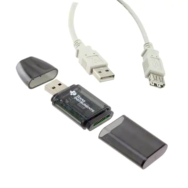
Table 1 summarizes the contents of the OPT3002EVM kit. Figure 1 shows the included hardware. Contact
the Texas Instruments Worldwide Customer Support Center nearest you if any component is missing. It is
highly recommended that you also check the OPT3002 product folder on the TI web site at www.ti.com to
verify you have the latest versions of the released software.
Table 1. Kit Contents
Item
Quantity
OPT3002 test board
1
SM-USB-DIG board
1
USB extension cable
1
Figure 1. Hardware Included With OPT3002EVM Kit
SBOU160 – May 2016
Submit Documentation Feedback
OPT3002EVM User's Guide
Copyright © 2016, Texas Instruments Incorporated
3
�Overview
1.2
www.ti.com
Related Documentation from Texas Instruments
The following documents provide information regarding Texas Instruments' integrated circuits used in the
assembly of the OPT3002EVM. This user's guide is available from the TI web site under literature number
SBOU160. Any letter appended to the literature number corresponds to the document revision that is
current at the time of the writing of this document. For the latest revision, click the link in Table 2. The
latest revision is also available from the TI website at www.ti.com, the Texas Instruments' Literature
Response Center at (800) 477-8924, and the Product Information Center at (972) 644-5580. When
ordering, identify the document by both title and literature number.
Table 2. Related Documentation
Document
2
Literature Number
OPT3002 product data sheet
SBOS745
SM-USB-DIG Platform user's guide
SBOU098
Hardware
Figure 2 shows the system setup for the OPT3002EVM. The computer runs the graphical user interface
(GUI) software that communicates with the SM-USB-DIG over a USB connection. The SM-USB-DIG
translates the USB commands from the computer into power, I2C, SPI™, and general-purpose
input/output (GPIO) commands for the OPT3002 test board. The OPT3002EVM does not require any
additional components to operate.
Figure 2. Hardware Setup
4
OPT3002EVM User's Guide
SBOU160 – May 2016
Submit Documentation Feedback
Copyright © 2016, Texas Instruments Incorporated
�Hardware
www.ti.com
2.1
Theory of Operation
A block diagram of the OPT3002 test board hardware is shown in Figure 3. The OPT3002 test board
contains connections for the power, I2C, and an interrupt signal. For evaluation purposes, the board also
has a 5-pin header that allows the OPT3002 test board to be connected to hardware other than the SMUSB-DIG Platform.
VDUT Supply
(Switched 3.3-V Power)
Interrupt
10-Pin, Female
SM-USB-DIG
Connector
OPT3002
Five
100-mil-Spaced
Test Points
I2C Interface
Figure 3. OPT3002 Test Board Block Diagram
2.2
Hardware Overview
If not already assembled, the basic hardware setup for the OPT3002EVM involves connecting the
OPT3002 test board to the SM-USB-DIG Platform, and then connecting the USB cable. This section
presents the details of this procedure.
CAUTION
Many of the components on the OPT3002EVM are susceptible to damage by
electrostatic discharge (ESD). Customers are advised to observe proper ESD
handling precautions when unpacking and handling the EVM, including the use
of a grounded wrist strap at an approved ESD workstation.
SBOU160 – May 2016
Submit Documentation Feedback
OPT3002EVM User's Guide
Copyright © 2016, Texas Instruments Incorporated
5
�Hardware
2.2.1
www.ti.com
Typical Hardware Setup
Connect the right-angle female socket on the OPT3002 test board to the right-angle male header on the
SM-USB-DIG Platform, as shown in Figure 4. Take special care to make sure that the two 10-pin sockets
directly align with each other. Plug the female USB-A cable to the SM-USB-DIG Platform, and then plug
the male USB-A cable into the computer.
NOTE:
Always connect the two boards together before connecting the USB cable to avoid any
issues if the connectors are misaligned.
Figure 4. Typical Hardware Connection
Figure 5 shows the typical response when the SM-USB-DIG is plugged into the USB port of the computer
for the first time. Typically, the computer responds with a Found New Hardware, USB Device pop-up
dialog window. The pop-up window then typically changes to Found New Hardware, USB Human Interface
Device. This pop-up indicates that the device is ready to be used. The SM-USB-DIG Platform uses the
human interface device drivers that are part of the Windows® operating system.
Figure 5. Typical Response After Connecting OPT3002EVM to the Computer
In some cases, the Add Hardware Wizard appears. If this installation prompt occurs, allow the device
manager to install the human interface device drivers by clicking Yes at each request to install the drivers.
6
OPT3002EVM User's Guide
SBOU160 – May 2016
Submit Documentation Feedback
Copyright © 2016, Texas Instruments Incorporated
�Software
www.ti.com
3
Software
This section describes the installation and operation of the OPT3002EVM software.
3.1
Hardware Requirements
The OPT3002EVM software has been tested on the Windows 7® operating system (OS) with United
States regional settings. The software should function correctly on other Windows operating systems.
3.2
Software Installation
The OPT3002EVM software is available through the OPT3002EVM Product Folder on the TI web site
(www.ti.com). To install the software to your computer, launch the OPT3002EVM installation file,
setup_OPT3002_EVM.exe.
The OPT3002EVM software then begins the installation process, as shown in Figure 6.
Figure 6. OPT3002EVM Software-Installation Launch
Follow the prompts shown in Figure 7 to install the OPT3002EVM software. After the prompts, the
OPT3002EVM GUI software completes installation.
Figure 7. Software-Installation Prompts
SBOU160 – May 2016
Submit Documentation Feedback
OPT3002EVM User's Guide
Copyright © 2016, Texas Instruments Incorporated
7
�Software
3.3
www.ti.com
Launching the Software
With the OPT3002EVM properly connected (see Figure 4), launch the EVM GUI software from the
Windows Start menu by navigating to the folder titled Texas Instruments and clicking on the OPT3002
EVM application. The software launches with a screen similar to that shown in Figure 8.
Figure 8. Main Operation Screen
If the message shown in Figure 9 appears when the OPT3002EVM GUI software is launched, disconnect
all components of the OPT3002EVM kit, and repeat the hardware assembly and connection instructions.
Figure 9. Hardware Error Message
8
OPT3002EVM User's Guide
SBOU160 – May 2016
Submit Documentation Feedback
Copyright © 2016, Texas Instruments Incorporated
�Software
www.ti.com
3.4
Software Operation
This section primarily discusses software operation and basic GUI functionality, and gives a description of
the various tabs.
3.4.1
Getting Started
With the hardware properly connected, and the EVM software installed and operating, make sure that the
power to the device is turned on by checking the LED on the SM-USB-DIG board and the VDUT indicator
on the SM-USB-DIG tab in the GUI software, as shown in Figure 10. The GUI has a primary window that
is used to configure and read from the OPT3002EVM, along with a secondary window used to access
different features of the OPT3002EVM.
Figure 10. Power Indicators
If the hardware address of the OPT3002EVM on the EVM board has not been reconfigured, then the
address fields shown on the SM-USB-DIG tab are set by default, as shown in Figure 11.
Figure 11. Default I2C Address Selection
To quickly start using the device, leave the default settings selected, click the Write Reg x01 button, and
then click the Run Continuously flip switch. The software then begins capturing data from the device. This
quick-start procedure is a good test to make sure everything is operational. To stop the computer from
capturing data and plotting, click Run Continuously again.
SBOU160 – May 2016
Submit Documentation Feedback
OPT3002EVM User's Guide
Copyright © 2016, Texas Instruments Incorporated
9
�Software
3.4.2
www.ti.com
Feature Descriptions
Register x00 is a read-only register that holds the range and converted value. These data are used (per
the OPT3002 data sheet) to compute the output, labeled Reg x00 in Figure 12. Click the Read Reg x00
button to update these fields and the plot with the latest values from the OPT3002EVM.
Figure 12. Register x00 Button and Recorded Values
Register x01 configures the OPT3002 device and provides feedback about the state of the device; the bit
names and full descriptions are shown in the OPT3002 data sheet. Figure 13 shows the control and status
register bits for register x01. All the configurable read-and-write bits have a drop-down menu to select the
appropriate value. All the read-only status bits have an associated small, blue indicator. Two buttons are
provided to operate register x01 because some of the bits have read and write capability. The Full Scale
Range selection field has four identical automatic range modes: 0x0C, 0x0D, 0x0E, and 0x0F. Also, the
Mode selection field has two identical continuous sampling options: 0x02 and 0x03.
Figure 13. Register x01 Control and Status Register Bits
Registers x02 and x03 enforce low and high limits, respectively, on the output ranges (exponent) and
values (mantissa) from the OPT3002. These registers are programmed using the appropriate fields, as
shown in Figure 14. Change the values of the data in these fields to write and read the values from the
OPT3002. No button press is required; however, make sure to exit the text field for the field to update.
Figure 14. Registers x02 and x03 LSB Limit Controls
There is a simulated screen backlight dimmer represented by a rectangle, shown in Figure 15. This
rectangle changes from black, through 254 shades of grey, to white, depending on the value of the output
measured by the OPT3002. The rectangle shows a brighter backlight for high-output situations, and a dim
backlight for low-output situations. The low limit (darkest backlight) is always 0, and the high limit
(brightest backlight) can be adjusted with the LSB for White numeric field.
Figure 15. Simulated Screen Backlight Dimmer
10
OPT3002EVM User's Guide
SBOU160 – May 2016
Submit Documentation Feedback
Copyright © 2016, Texas Instruments Incorporated
�Software
www.ti.com
The software provides a plot of the register x01 output labeled Weighted LSB vs. Sample Number, as
shown in Figure 16. As readings are collected, the plot is updated with those values. The y-axis is
autoscaled to show the magnitude of the output value recorded, and has a visible history of 100 samples
along the x-axis. To reset the plot, return to the SM-USB-DIG tab and click the Re-Initialize button, as
shown in Figure 17. To access the plot axis range and formatting, right-click the plot.
Figure 16. Weighted LSB vs. Sample Number Plot
Figure 17. Re-Initialize Button
SBOU160 – May 2016
Submit Documentation Feedback
OPT3002EVM User's Guide
Copyright © 2016, Texas Instruments Incorporated
11
�Schematic, PCB Layout, and Bill of Materials
www.ti.com
There is a data logging feature included in the software that recorda the date and time from the host
computer, along with the measured value reported by the device. After a destination file is selected by
clicking Select a File/Path, as shown in Figure 18, turn on the Logging On/Off selector switch to append
data to that file in .tab format.
Figure 18. Data Logging Setup and Enable
4
Schematic, PCB Layout, and Bill of Materials
4.1
Schematic
Figure 19 shows the complete schematic of the OPT3002 test board. SDA and SCK are pulled up by the
SM-USB-DIG Platform; therefore, there are no pull-up resistors present on the board. R2 is a pull-up
resistor for the interrupt signal, C1 is a bypass capacitor for VDUT, and R4 is a jumper to tie the address
pin to ground. If another address is desired, remove R4 and install a wire to the pad or via, and then to the
appropriate signal source.
J2
GND
1
2
3
4
5
SCK
INT
SDA
VDUT
GND
VDUT
SDA
INT
SCK
SM-USB-DIG Header
J1
1
2
3
4
5
6
7
8
9
10
R1 R2 R3
DNP
DNP
10k 10k
10k
1
VDUT
VDD
C1
0.1µF
SCL
SDA
INT
ADDR
GND
PAD
4
6
5
2
3
7
SCK
SDA
INT
R4
0
U1
GND
Figure 19. OPT3002 Test-Board Schematic
The OPT3002 is mounted on the back side of the board; therefore, the LED light from the SM-USB-DIG is
directed away from the device. Also, no additional LEDs are installed on the test board in order to reduce
total ambient light around the device. The back side of the board is mostly planar; mounting holes are
included to accommodate evaluation.
12
OPT3002EVM User's Guide
SBOU160 – May 2016
Submit Documentation Feedback
Copyright © 2016, Texas Instruments Incorporated
�Schematic, PCB Layout, and Bill of Materials
www.ti.com
4.2
PCB Layout
Figure 20 and Figure 21 show the top and bottom PCB layers of the test board, respectively. Figure 22
and Figure 23 show the assembly drawings of the top and bottom PCB layers, respectively.
Figure 20. PCB Top Layer
Figure 21. PCB Bottom Layer
SBOU160 – May 2016
Submit Documentation Feedback
OPT3002EVM User's Guide
Copyright © 2016, Texas Instruments Incorporated
13
�Schematic, PCB Layout, and Bill of Materials
www.ti.com
Figure 22. PCB Top-Layer Assembly Drawing
Figure 23. PCB Bottom-Layer Assembly Drawing
4.3
Bill of Materials
Table 3 lists the bill of materials for the OPT3002 test board.
Table 3. OPT3002 Test Board Parts List
14
Qty
RefDes
1
C1
CAP, CERM, 0.1uF, 50V, +/-10%, X7R, 0805
Description
08055C104KAT2A
AVX Corp.
1
J1
Receptacle, 50mil 10x1, R/A, TH
851-43-010-20-001000
Mill-Max
1
R2
RES, 10k ohm, 5%, 0.125W, 0805
CRCW080510K0JNEA
Vishay Dale
1
R4
RES, 0 ohm, 5%, 0.125W, 0805
CRCW08050000Z0EA
Vishay Dale
1
U1
Light Sensor, DNP0006A
OPT3002DNP
Texas Instruments
OPT3002EVM User's Guide
Part Number
MFR
SBOU160 – May 2016
Submit Documentation Feedback
Copyright © 2016, Texas Instruments Incorporated
�STANDARD TERMS AND CONDITIONS FOR EVALUATION MODULES
1.
Delivery: TI delivers TI evaluation boards, kits, or modules, including any accompanying demonstration software, components, or
documentation (collectively, an “EVM” or “EVMs”) to the User (“User”) in accordance with the terms and conditions set forth herein.
Acceptance of the EVM is expressly subject to the following terms and conditions.
1.1 EVMs are intended solely for product or software developers for use in a research and development setting to facilitate feasibility
evaluation, experimentation, or scientific analysis of TI semiconductors products. EVMs have no direct function and are not
finished products. EVMs shall not be directly or indirectly assembled as a part or subassembly in any finished product. For
clarification, any software or software tools provided with the EVM (“Software”) shall not be subject to the terms and conditions
set forth herein but rather shall be subject to the applicable terms and conditions that accompany such Software
1.2 EVMs are not intended for consumer or household use. EVMs may not be sold, sublicensed, leased, rented, loaned, assigned,
or otherwise distributed for commercial purposes by Users, in whole or in part, or used in any finished product or production
system.
2
Limited Warranty and Related Remedies/Disclaimers:
2.1 These terms and conditions do not apply to Software. The warranty, if any, for Software is covered in the applicable Software
License Agreement.
2.2 TI warrants that the TI EVM will conform to TI's published specifications for ninety (90) days after the date TI delivers such EVM
to User. Notwithstanding the foregoing, TI shall not be liable for any defects that are caused by neglect, misuse or mistreatment
by an entity other than TI, including improper installation or testing, or for any EVMs that have been altered or modified in any
way by an entity other than TI. Moreover, TI shall not be liable for any defects that result from User's design, specifications or
instructions for such EVMs. Testing and other quality control techniques are used to the extent TI deems necessary or as
mandated by government requirements. TI does not test all parameters of each EVM.
2.3 If any EVM fails to conform to the warranty set forth above, TI's sole liability shall be at its option to repair or replace such EVM,
or credit User's account for such EVM. TI's liability under this warranty shall be limited to EVMs that are returned during the
warranty period to the address designated by TI and that are determined by TI not to conform to such warranty. If TI elects to
repair or replace such EVM, TI shall have a reasonable time to repair such EVM or provide replacements. Repaired EVMs shall
be warranted for the remainder of the original warranty period. Replaced EVMs shall be warranted for a new full ninety (90) day
warranty period.
3
Regulatory Notices:
3.1 United States
3.1.1
Notice applicable to EVMs not FCC-Approved:
This kit is designed to allow product developers to evaluate electronic components, circuitry, or software associated with the kit
to determine whether to incorporate such items in a finished product and software developers to write software applications for
use with the end product. This kit is not a finished product and when assembled may not be resold or otherwise marketed unless
all required FCC equipment authorizations are first obtained. Operation is subject to the condition that this product not cause
harmful interference to licensed radio stations and that this product accept harmful interference. Unless the assembled kit is
designed to operate under part 15, part 18 or part 95 of this chapter, the operator of the kit must operate under the authority of
an FCC license holder or must secure an experimental authorization under part 5 of this chapter.
3.1.2
For EVMs annotated as FCC – FEDERAL COMMUNICATIONS COMMISSION Part 15 Compliant:
CAUTION
This device complies with part 15 of the FCC Rules. Operation is subject to the following two conditions: (1) This device may not
cause harmful interference, and (2) this device must accept any interference received, including interference that may cause
undesired operation.
Changes or modifications not expressly approved by the party responsible for compliance could void the user's authority to
operate the equipment.
FCC Interference Statement for Class A EVM devices
NOTE: This equipment has been tested and found to comply with the limits for a Class A digital device, pursuant to part 15 of
the FCC Rules. These limits are designed to provide reasonable protection against harmful interference when the equipment is
operated in a commercial environment. This equipment generates, uses, and can radiate radio frequency energy and, if not
installed and used in accordance with the instruction manual, may cause harmful interference to radio communications.
Operation of this equipment in a residential area is likely to cause harmful interference in which case the user will be required to
correct the interference at his own expense.
SPACER
SPACER
SPACER
SPACER
SPACER
SPACER
SPACER
SPACER
�FCC Interference Statement for Class B EVM devices
NOTE: This equipment has been tested and found to comply with the limits for a Class B digital device, pursuant to part 15 of
the FCC Rules. These limits are designed to provide reasonable protection against harmful interference in a residential
installation. This equipment generates, uses and can radiate radio frequency energy and, if not installed and used in accordance
with the instructions, may cause harmful interference to radio communications. However, there is no guarantee that interference
will not occur in a particular installation. If this equipment does cause harmful interference to radio or television reception, which
can be determined by turning the equipment off and on, the user is encouraged to try to correct the interference by one or more
of the following measures:
•
•
•
•
Reorient or relocate the receiving antenna.
Increase the separation between the equipment and receiver.
Connect the equipment into an outlet on a circuit different from that to which the receiver is connected.
Consult the dealer or an experienced radio/TV technician for help.
3.2 Canada
3.2.1
For EVMs issued with an Industry Canada Certificate of Conformance to RSS-210
Concerning EVMs Including Radio Transmitters:
This device complies with Industry Canada license-exempt RSS standard(s). Operation is subject to the following two conditions:
(1) this device may not cause interference, and (2) this device must accept any interference, including interference that may
cause undesired operation of the device.
Concernant les EVMs avec appareils radio:
Le présent appareil est conforme aux CNR d'Industrie Canada applicables aux appareils radio exempts de licence. L'exploitation
est autorisée aux deux conditions suivantes: (1) l'appareil ne doit pas produire de brouillage, et (2) l'utilisateur de l'appareil doit
accepter tout brouillage radioélectrique subi, même si le brouillage est susceptible d'en compromettre le fonctionnement.
Concerning EVMs Including Detachable Antennas:
Under Industry Canada regulations, this radio transmitter may only operate using an antenna of a type and maximum (or lesser)
gain approved for the transmitter by Industry Canada. To reduce potential radio interference to other users, the antenna type
and its gain should be so chosen that the equivalent isotropically radiated power (e.i.r.p.) is not more than that necessary for
successful communication. This radio transmitter has been approved by Industry Canada to operate with the antenna types
listed in the user guide with the maximum permissible gain and required antenna impedance for each antenna type indicated.
Antenna types not included in this list, having a gain greater than the maximum gain indicated for that type, are strictly prohibited
for use with this device.
Concernant les EVMs avec antennes détachables
Conformément à la réglementation d'Industrie Canada, le présent émetteur radio peut fonctionner avec une antenne d'un type et
d'un gain maximal (ou inférieur) approuvé pour l'émetteur par Industrie Canada. Dans le but de réduire les risques de brouillage
radioélectrique à l'intention des autres utilisateurs, il faut choisir le type d'antenne et son gain de sorte que la puissance isotrope
rayonnée équivalente (p.i.r.e.) ne dépasse pas l'intensité nécessaire à l'établissement d'une communication satisfaisante. Le
présent émetteur radio a été approuvé par Industrie Canada pour fonctionner avec les types d'antenne énumérés dans le
manuel d’usage et ayant un gain admissible maximal et l'impédance requise pour chaque type d'antenne. Les types d'antenne
non inclus dans cette liste, ou dont le gain est supérieur au gain maximal indiqué, sont strictement interdits pour l'exploitation de
l'émetteur
3.3 Japan
3.3.1
Notice for EVMs delivered in Japan: Please see http://www.tij.co.jp/lsds/ti_ja/general/eStore/notice_01.page 日本国内に
輸入される評価用キット、ボードについては、次のところをご覧ください。
http://www.tij.co.jp/lsds/ti_ja/general/eStore/notice_01.page
3.3.2
Notice for Users of EVMs Considered “Radio Frequency Products” in Japan: EVMs entering Japan may not be certified
by TI as conforming to Technical Regulations of Radio Law of Japan.
If User uses EVMs in Japan, not certified to Technical Regulations of Radio Law of Japan, User is required by Radio Law of
Japan to follow the instructions below with respect to EVMs:
1.
2.
3.
Use EVMs in a shielded room or any other test facility as defined in the notification #173 issued by Ministry of Internal
Affairs and Communications on March 28, 2006, based on Sub-section 1.1 of Article 6 of the Ministry’s Rule for
Enforcement of Radio Law of Japan,
Use EVMs only after User obtains the license of Test Radio Station as provided in Radio Law of Japan with respect to
EVMs, or
Use of EVMs only after User obtains the Technical Regulations Conformity Certification as provided in Radio Law of Japan
with respect to EVMs. Also, do not transfer EVMs, unless User gives the same notice above to the transferee. Please note
that if User does not follow the instructions above, User will be subject to penalties of Radio Law of Japan.
SPACER
SPACER
SPACER
SPACER
SPACER
�【無線電波を送信する製品の開発キットをお使いになる際の注意事項】 開発キットの中には技術基準適合証明を受けて
いないものがあります。 技術適合証明を受けていないもののご使用に際しては、電波法遵守のため、以下のいずれかの
措置を取っていただく必要がありますのでご注意ください。
1.
2.
3.
電波法施行規則第6条第1項第1号に基づく平成18年3月28日総務省告示第173号で定められた電波暗室等の試験設備でご使用
いただく。
実験局の免許を取得後ご使用いただく。
技術基準適合証明を取得後ご使用いただく。
なお、本製品は、上記の「ご使用にあたっての注意」を譲渡先、移転先に通知しない限り、譲渡、移転できないものとします。
上記を遵守頂けない場合は、電波法の罰則が適用される可能性があることをご留意ください。 日本テキサス・イ
ンスツルメンツ株式会社
東京都新宿区西新宿6丁目24番1号
西新宿三井ビル
3.3.3
Notice for EVMs for Power Line Communication: Please see http://www.tij.co.jp/lsds/ti_ja/general/eStore/notice_02.page
電力線搬送波通信についての開発キットをお使いになる際の注意事項については、次のところをご覧くださ
い。http://www.tij.co.jp/lsds/ti_ja/general/eStore/notice_02.page
SPACER
4
EVM Use Restrictions and Warnings:
4.1 EVMS ARE NOT FOR USE IN FUNCTIONAL SAFETY AND/OR SAFETY CRITICAL EVALUATIONS, INCLUDING BUT NOT
LIMITED TO EVALUATIONS OF LIFE SUPPORT APPLICATIONS.
4.2 User must read and apply the user guide and other available documentation provided by TI regarding the EVM prior to handling
or using the EVM, including without limitation any warning or restriction notices. The notices contain important safety information
related to, for example, temperatures and voltages.
4.3 Safety-Related Warnings and Restrictions:
4.3.1
User shall operate the EVM within TI’s recommended specifications and environmental considerations stated in the user
guide, other available documentation provided by TI, and any other applicable requirements and employ reasonable and
customary safeguards. Exceeding the specified performance ratings and specifications (including but not limited to input
and output voltage, current, power, and environmental ranges) for the EVM may cause personal injury or death, or
property damage. If there are questions concerning performance ratings and specifications, User should contact a TI
field representative prior to connecting interface electronics including input power and intended loads. Any loads applied
outside of the specified output range may also result in unintended and/or inaccurate operation and/or possible
permanent damage to the EVM and/or interface electronics. Please consult the EVM user guide prior to connecting any
load to the EVM output. If there is uncertainty as to the load specification, please contact a TI field representative.
During normal operation, even with the inputs and outputs kept within the specified allowable ranges, some circuit
components may have elevated case temperatures. These components include but are not limited to linear regulators,
switching transistors, pass transistors, current sense resistors, and heat sinks, which can be identified using the
information in the associated documentation. When working with the EVM, please be aware that the EVM may become
very warm.
4.3.2
EVMs are intended solely for use by technically qualified, professional electronics experts who are familiar with the
dangers and application risks associated with handling electrical mechanical components, systems, and subsystems.
User assumes all responsibility and liability for proper and safe handling and use of the EVM by User or its employees,
affiliates, contractors or designees. User assumes all responsibility and liability to ensure that any interfaces (electronic
and/or mechanical) between the EVM and any human body are designed with suitable isolation and means to safely
limit accessible leakage currents to minimize the risk of electrical shock hazard. User assumes all responsibility and
liability for any improper or unsafe handling or use of the EVM by User or its employees, affiliates, contractors or
designees.
4.4 User assumes all responsibility and liability to determine whether the EVM is subject to any applicable international, federal,
state, or local laws and regulations related to User’s handling and use of the EVM and, if applicable, User assumes all
responsibility and liability for compliance in all respects with such laws and regulations. User assumes all responsibility and
liability for proper disposal and recycling of the EVM consistent with all applicable international, federal, state, and local
requirements.
5.
Accuracy of Information: To the extent TI provides information on the availability and function of EVMs, TI attempts to be as accurate
as possible. However, TI does not warrant the accuracy of EVM descriptions, EVM availability or other information on its websites as
accurate, complete, reliable, current, or error-free.
SPACER
SPACER
SPACER
SPACER
SPACER
SPACER
�SPACER
6.
Disclaimers:
6.1 EXCEPT AS SET FORTH ABOVE, EVMS AND ANY WRITTEN DESIGN MATERIALS PROVIDED WITH THE EVM (AND THE
DESIGN OF THE EVM ITSELF) ARE PROVIDED "AS IS" AND "WITH ALL FAULTS." TI DISCLAIMS ALL OTHER
WARRANTIES, EXPRESS OR IMPLIED, REGARDING SUCH ITEMS, INCLUDING BUT NOT LIMITED TO ANY IMPLIED
WARRANTIES OF MERCHANTABILITY OR FITNESS FOR A PARTICULAR PURPOSE OR NON-INFRINGEMENT OF ANY
THIRD PARTY PATENTS, COPYRIGHTS, TRADE SECRETS OR OTHER INTELLECTUAL PROPERTY RIGHTS.
6.2 EXCEPT FOR THE LIMITED RIGHT TO USE THE EVM SET FORTH HEREIN, NOTHING IN THESE TERMS AND
CONDITIONS SHALL BE CONSTRUED AS GRANTING OR CONFERRING ANY RIGHTS BY LICENSE, PATENT, OR ANY
OTHER INDUSTRIAL OR INTELLECTUAL PROPERTY RIGHT OF TI, ITS SUPPLIERS/LICENSORS OR ANY OTHER THIRD
PARTY, TO USE THE EVM IN ANY FINISHED END-USER OR READY-TO-USE FINAL PRODUCT, OR FOR ANY
INVENTION, DISCOVERY OR IMPROVEMENT MADE, CONCEIVED OR ACQUIRED PRIOR TO OR AFTER DELIVERY OF
THE EVM.
7.
USER'S INDEMNITY OBLIGATIONS AND REPRESENTATIONS. USER WILL DEFEND, INDEMNIFY AND HOLD TI, ITS
LICENSORS AND THEIR REPRESENTATIVES HARMLESS FROM AND AGAINST ANY AND ALL CLAIMS, DAMAGES, LOSSES,
EXPENSES, COSTS AND LIABILITIES (COLLECTIVELY, "CLAIMS") ARISING OUT OF OR IN CONNECTION WITH ANY
HANDLING OR USE OF THE EVM THAT IS NOT IN ACCORDANCE WITH THESE TERMS AND CONDITIONS. THIS OBLIGATION
SHALL APPLY WHETHER CLAIMS ARISE UNDER STATUTE, REGULATION, OR THE LAW OF TORT, CONTRACT OR ANY
OTHER LEGAL THEORY, AND EVEN IF THE EVM FAILS TO PERFORM AS DESCRIBED OR EXPECTED.
8.
Limitations on Damages and Liability:
8.1 General Limitations. IN NO EVENT SHALL TI BE LIABLE FOR ANY SPECIAL, COLLATERAL, INDIRECT, PUNITIVE,
INCIDENTAL, CONSEQUENTIAL, OR EXEMPLARY DAMAGES IN CONNECTION WITH OR ARISING OUT OF THESE
TERMS ANDCONDITIONS OR THE USE OF THE EVMS PROVIDED HEREUNDER, REGARDLESS OF WHETHER TI HAS
BEEN ADVISED OF THE POSSIBILITY OF SUCH DAMAGES. EXCLUDED DAMAGES INCLUDE, BUT ARE NOT LIMITED
TO, COST OF REMOVAL OR REINSTALLATION, ANCILLARY COSTS TO THE PROCUREMENT OF SUBSTITUTE GOODS
OR SERVICES, RETESTING, OUTSIDE COMPUTER TIME, LABOR COSTS, LOSS OF GOODWILL, LOSS OF PROFITS,
LOSS OF SAVINGS, LOSS OF USE, LOSS OF DATA, OR BUSINESS INTERRUPTION. NO CLAIM, SUIT OR ACTION SHALL
BE BROUGHT AGAINST TI MORE THAN ONE YEAR AFTER THE RELATED CAUSE OF ACTION HAS OCCURRED.
8.2 Specific Limitations. IN NO EVENT SHALL TI'S AGGREGATE LIABILITY FROM ANY WARRANTY OR OTHER OBLIGATION
ARISING OUT OF OR IN CONNECTION WITH THESE TERMS AND CONDITIONS, OR ANY USE OF ANY TI EVM
PROVIDED HEREUNDER, EXCEED THE TOTAL AMOUNT PAID TO TI FOR THE PARTICULAR UNITS SOLD UNDER
THESE TERMS AND CONDITIONS WITH RESPECT TO WHICH LOSSES OR DAMAGES ARE CLAIMED. THE EXISTENCE
OF MORE THAN ONE CLAIM AGAINST THE PARTICULAR UNITS SOLD TO USER UNDER THESE TERMS AND
CONDITIONS SHALL NOT ENLARGE OR EXTEND THIS LIMIT.
9.
Return Policy. Except as otherwise provided, TI does not offer any refunds, returns, or exchanges. Furthermore, no return of EVM(s)
will be accepted if the package has been opened and no return of the EVM(s) will be accepted if they are damaged or otherwise not in
a resalable condition. If User feels it has been incorrectly charged for the EVM(s) it ordered or that delivery violates the applicable
order, User should contact TI. All refunds will be made in full within thirty (30) working days from the return of the components(s),
excluding any postage or packaging costs.
10. Governing Law: These terms and conditions shall be governed by and interpreted in accordance with the laws of the State of Texas,
without reference to conflict-of-laws principles. User agrees that non-exclusive jurisdiction for any dispute arising out of or relating to
these terms and conditions lies within courts located in the State of Texas and consents to venue in Dallas County, Texas.
Notwithstanding the foregoing, any judgment may be enforced in any United States or foreign court, and TI may seek injunctive relief
in any United States or foreign court.
Mailing Address: Texas Instruments, Post Office Box 655303, Dallas, Texas 75265
Copyright © 2015, Texas Instruments Incorporated
spacer
�IMPORTANT NOTICE
Texas Instruments Incorporated and its subsidiaries (TI) reserve the right to make corrections, enhancements, improvements and other
changes to its semiconductor products and services per JESD46, latest issue, and to discontinue any product or service per JESD48, latest
issue. Buyers should obtain the latest relevant information before placing orders and should verify that such information is current and
complete. All semiconductor products (also referred to herein as “components”) are sold subject to TI’s terms and conditions of sale
supplied at the time of order acknowledgment.
TI warrants performance of its components to the specifications applicable at the time of sale, in accordance with the warranty in TI’s terms
and conditions of sale of semiconductor products. Testing and other quality control techniques are used to the extent TI deems necessary
to support this warranty. Except where mandated by applicable law, testing of all parameters of each component is not necessarily
performed.
TI assumes no liability for applications assistance or the design of Buyers’ products. Buyers are responsible for their products and
applications using TI components. To minimize the risks associated with Buyers’ products and applications, Buyers should provide
adequate design and operating safeguards.
TI does not warrant or represent that any license, either express or implied, is granted under any patent right, copyright, mask work right, or
other intellectual property right relating to any combination, machine, or process in which TI components or services are used. Information
published by TI regarding third-party products or services does not constitute a license to use such products or services or a warranty or
endorsement thereof. Use of such information may require a license from a third party under the patents or other intellectual property of the
third party, or a license from TI under the patents or other intellectual property of TI.
Reproduction of significant portions of TI information in TI data books or data sheets is permissible only if reproduction is without alteration
and is accompanied by all associated warranties, conditions, limitations, and notices. TI is not responsible or liable for such altered
documentation. Information of third parties may be subject to additional restrictions.
Resale of TI components or services with statements different from or beyond the parameters stated by TI for that component or service
voids all express and any implied warranties for the associated TI component or service and is an unfair and deceptive business practice.
TI is not responsible or liable for any such statements.
Buyer acknowledges and agrees that it is solely responsible for compliance with all legal, regulatory and safety-related requirements
concerning its products, and any use of TI components in its applications, notwithstanding any applications-related information or support
that may be provided by TI. Buyer represents and agrees that it has all the necessary expertise to create and implement safeguards which
anticipate dangerous consequences of failures, monitor failures and their consequences, lessen the likelihood of failures that might cause
harm and take appropriate remedial actions. Buyer will fully indemnify TI and its representatives against any damages arising out of the use
of any TI components in safety-critical applications.
In some cases, TI components may be promoted specifically to facilitate safety-related applications. With such components, TI’s goal is to
help enable customers to design and create their own end-product solutions that meet applicable functional safety standards and
requirements. Nonetheless, such components are subject to these terms.
No TI components are authorized for use in FDA Class III (or similar life-critical medical equipment) unless authorized officers of the parties
have executed a special agreement specifically governing such use.
Only those TI components which TI has specifically designated as military grade or “enhanced plastic” are designed and intended for use in
military/aerospace applications or environments. Buyer acknowledges and agrees that any military or aerospace use of TI components
which have not been so designated is solely at the Buyer's risk, and that Buyer is solely responsible for compliance with all legal and
regulatory requirements in connection with such use.
TI has specifically designated certain components as meeting ISO/TS16949 requirements, mainly for automotive use. In any case of use of
non-designated products, TI will not be responsible for any failure to meet ISO/TS16949.
Products
Applications
Audio
www.ti.com/audio
Automotive and Transportation
www.ti.com/automotive
Amplifiers
amplifier.ti.com
Communications and Telecom
www.ti.com/communications
Data Converters
dataconverter.ti.com
Computers and Peripherals
www.ti.com/computers
DLP® Products
www.dlp.com
Consumer Electronics
www.ti.com/consumer-apps
DSP
dsp.ti.com
Energy and Lighting
www.ti.com/energy
Clocks and Timers
www.ti.com/clocks
Industrial
www.ti.com/industrial
Interface
interface.ti.com
Medical
www.ti.com/medical
Logic
logic.ti.com
Security
www.ti.com/security
Power Mgmt
power.ti.com
Space, Avionics and Defense
www.ti.com/space-avionics-defense
Microcontrollers
microcontroller.ti.com
Video and Imaging
www.ti.com/video
RFID
www.ti-rfid.com
OMAP Applications Processors
www.ti.com/omap
TI E2E Community
e2e.ti.com
Wireless Connectivity
www.ti.com/wirelessconnectivity
Mailing Address: Texas Instruments, Post Office Box 655303, Dallas, Texas 75265
Copyright © 2016, Texas Instruments Incorporated
�


 工商网监
湘ICP备2023018690号
工商网监
湘ICP备2023018690号
