Product
Folder
Sample &
Buy
Support &
Community
Tools &
Software
Technical
Documents
PCM1794A
SLES117B – AUGUST 2004 – REVISED DECEMBER 2015
PCM1794A 24-Bit, 192-kHz Sampling, Advanced Segment, Audio Stereo
Digital-to-Analog Converter
1 Features
2 Applications
•
•
•
•
•
•
•
1
•
•
•
•
•
•
•
•
•
•
•
•
•
•
24-Bit Resolution
Analog Performance:
– Dynamic Range:
– 132 dB (9 V RMS, Mono)
– 129 dB (4.5 V RMS, Stereo)
– 127 dB (2 V RMS, Stereo)
– THD+N: 0.0004%
Differential Current Output: 7.8 mA p-p
8× Oversampling Digital Filter:
– Stop-Band Attenuation: –130 dB
– Pass-Band Ripple: ±0.00001 dB
Sampling Frequency: 10 kHz to 200 kHz
System Clock: 128, 192, 256, 384, 512, or 768 fS
With Autodetect
Accepts 16-Bit and 24-Bit Audio Data
PCM Data Formats: Standard, I2S, and LeftJustified
Optional Interface Available to External Digital
Filter or DSP
Digital De-Emphasis
Digital Filter Rolloff: Sharp or Slow
Soft Mute
Zero Flag
Dual-Supply Operation: 5-V Analog, 3.3-V Digital
5-V Tolerant Digital Inputs
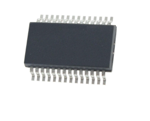
Small 28-Pin SSOP Package
A/V Receivers
DVD Players
Musical Instruments
Car Audio Systems
Other Applications Requiring 24-Bit Audio
3 Description
The PCM1794A device is a monolithic, CMOSintegrated circuit that includes stereo digital-to-analog
converters (DACs) and support circuitry in a small 28pin SSOP package. The data converters use TI’s
advanced segment DAC architecture to achieve
excellent dynamic performance and improved
tolerance to clock jitter. The PCM1794A device
provides balanced current outputs, allowing the user
to optimize analog performance externally. Sampling
rates up to 200 kHz are supported.
Device Information(1)
PART NUMBER
PCM1794A
PACKAGE
SSOP (28)
BODY SIZE (NOM)
10.20 mm × 5.30 mm
(1) For all available packages, see the orderable addendum at
the end of the data sheet.
Simplified Application Diagram
I/V Stage
Data
L Analog Out
LRCK
DSP
BCK
Differential Output or
Differential to SE
Stage
PCM1794A
MCLK
R Analog Out
I/V Stage
1
An IMPORTANT NOTICE at the end of this data sheet addresses availability, warranty, changes, use in safety-critical applications,
intellectual property matters and other important disclaimers. PRODUCTION DATA.
�PCM1794A
SLES117B – AUGUST 2004 – REVISED DECEMBER 2015
www.ti.com
Table of Contents
1
2
3
4
5
6
7
Features ..................................................................
Applications ...........................................................
Description .............................................................
Revision History.....................................................
Pin Configuration and Functions .........................
Specifications.........................................................
1
1
1
2
3
4
6.1
6.2
6.3
6.4
6.5
6.6
6.7
4
4
5
5
5
7
9
Absolute Maximum Ratings ......................................
ESD Ratings..............................................................
Recommended Operating Conditions.......................
Thermal Information ..................................................
Electrical Characteristics...........................................
Timing Requirements ................................................
Typical Characteristics ..............................................
Detailed Description ............................................ 12
7.1 Overview ................................................................. 12
7.2 Functional Block Diagram ....................................... 12
7.3 Feature Description................................................. 13
7.4 Device Functional Modes........................................ 18
8
Application and Implementation ........................ 19
8.1 Application Information............................................ 19
8.2 Typical Application ................................................. 25
9 Power Supply Recommendations...................... 26
10 Layout................................................................... 26
10.1 Layout Guidelines ................................................. 26
10.2 Layout Example .................................................... 27
11 Device and Documentation Support ................. 28
11.1
11.2
11.3
11.4
11.5
Documentation Support ........................................
Community Resources..........................................
Trademarks ...........................................................
Electrostatic Discharge Caution ............................
Glossary ................................................................
28
28
28
28
28
12 Mechanical, Packaging, and Orderable
Information ........................................................... 28
4 Revision History
NOTE: Page numbers for previous revisions may differ from page numbers in the current version.
Changes from Revision A (November 2006) to Revision B
•
2
Page
Added ESD Ratings table, Feature Description section, Device Functional Modes, Application and Implementation
section, Power Supply Recommendations section, Layout section, Device and Documentation Support section, and
Mechanical, Packaging, and Orderable Information section. ................................................................................................ 1
Submit Documentation Feedback
Copyright © 2004–2015, Texas Instruments Incorporated
Product Folder Links: PCM1794A
�PCM1794A
www.ti.com
SLES117B – AUGUST 2004 – REVISED DECEMBER 2015
5 Pin Configuration and Functions
DB Package
28-Pin SSOP
Top View
MONO
1
28
VCC2L
CHSL
2
27
AGND3L
DEM
3
26
IOUTL–
LRCK
4
25
IOUTL+
DATA
5
24
AGND2
BCK
6
23
VCC1
SCK
7
22
VCOML
DGND
8
21
VCOMR
VDD
9
20
IREF
MUTE
10
19
AGND1
FMT0
11
18
IOUTR–
FMT1
12
17
IOUTR+
ZERO
13
16
AGND3R
RST
14
15
VCC2R
Pin Functions
PIN
I/O
DESCRIPTION
NO.
NAME
1
MONO
I
Monaural mode enable (1)
2
CHSL
I
L-channel, R-channel select (1)
3
DEM
I
De-emphasis enable (1)
4
LRCK
I
Left and right clock (fS) input (1)
5
DATA
I
Serial audio data input (1)
6
BCK
I
Bit clock input (1)
7
SCK
I
System clock input (1)
8
DGND
—
Digital ground
9
VDD
—
Digital power supply, 3.3 V
10
MUTE
I
Mute control (1)
11
FMT0
I
Audio data format select (1)
12
FMT1
I
Audio data format select (1)
13
ZERO
O
Zero flag
14
RST
I
Reset (1)
15
VCC2R
—
Analog power supply (R-channel DAC), 5 V
16
AGND3R
—
Analog ground (R-channel DAC)
17
IOUTR+
O
R-channel analog current output +
18
IOUTR–
O
R-channel analog current output –
19
AGND1
—
Analog ground (internal bias)
20
IREF
—
Output current reference bias pin
21
VCOMR
—
R-channel internal bias decoupling pin
22
VCOML
—
L-channel internal bias decoupling pin
(1)
Schmitt-trigger input, 5-V tolerant.
Submit Documentation Feedback
Copyright © 2004–2015, Texas Instruments Incorporated
Product Folder Links: PCM1794A
3
�PCM1794A
SLES117B – AUGUST 2004 – REVISED DECEMBER 2015
www.ti.com
Pin Functions (continued)
PIN
NO.
NAME
I/O
DESCRIPTION
23
VCC1
—
Analog power supply, 5 V
24
AGND2
—
Analog ground (internal bias)
25
IOUTL+
O
L-channel analog current output +
26
IOUTL–
O
L-channel analog current output –
27
AGND3L
—
Analog ground (L-channel DAC)
28
VCC2L
—
Analog power supply (L-channel DAC), 5 V
6 Specifications
6.1 Absolute Maximum Ratings
over operating free-air temperature range (unless otherwise noted)
Supply Voltage
(1)
MIN
MAX
VCC1, VCC2L, VCC2R
–0.3
6.5
VDD
–0.3
4
UNIT
V
Supply voltage differences: VCC1, VCC2L, VCC2R
±0.1
V
Ground voltage differences: AGND1, AGND2, AGND3L, AGND3R, DGND
±0.1
V
LRCK, DATA, BCK, SCK, FMT1,
FMT0, MONO, CHSL, DEM, MUTE,
RST
–0.3
ZERO
–0.3
(VDD + 0.3 V) < 4
–0.3
(VCC + 0.3 V) < 6.5
V
±10
mA
125
°C
Junction temperature
150
°C
Lead temperature (soldering, 5 s)
260
°C
Package temperature (IR reflow, peak)
250
°C
150
°C
Digital input voltage
Analog input voltage
Input current (any pins except supplies)
Ambient temperature under bias
–40
Storage temperature, Tstg
(1)
–55
6.5
V
Stresses beyond those listed under Absolute Maximum Ratings may cause permanent damage to the device. These are stress ratings
only, which do not imply functional operation of the device at these or any other conditions beyond those indicated under Recommended
Operating Conditions. Exposure to absolute-maximum-rated conditions for extended periods may affect device reliability.
6.2 ESD Ratings
VALUE
V(ESD)
(1)
(2)
4
Electrostatic discharge
Human-body model (HBM), per ANSI/ESDA/JEDEC JS-001 (1)
±2500
Charged-device model (CDM), per JEDEC specification JESD22C101 (2)
±1500
UNIT
V
JEDEC document JEP155 states that 500-V HBM allows safe manufacturing with a standard ESD control process.
JEDEC document JEP157 states that 250-V CDM allows safe manufacturing with a standard ESD control process.
Submit Documentation Feedback
Copyright © 2004–2015, Texas Instruments Incorporated
Product Folder Links: PCM1794A
�PCM1794A
www.ti.com
SLES117B – AUGUST 2004 – REVISED DECEMBER 2015
6.3 Recommended Operating Conditions
over operating free-air temperature range (unless otherwise noted)
VDD
VCC1
VCC2L
VCC2R
Supply voltage
TJ
Operation temperature
MIN
NOM
MAX
UNIT
3
3.3
3.6
VDC
4.75
5
5.25
VDC
—25
85
°C
6.4 Thermal Information
PCM1794A
THERMAL METRIC (1)
DB (SSOP)
UNIT
28 PINS
RθJA
Junction-to-ambient thermal resistance
66.4
°C/W
RθJC(top)
Junction-to-case (top) thermal resistance
25.4
°C/W
RθJB
Junction-to-board thermal resistance
27.5
°C/W
ψJT
Junction-to-top characterization parameter
2.3
°C/W
ψJB
Junction-to-board characterization parameter
27.1
°C/W
RθJC(bot)
Junction-to-case (bottom) thermal resistance
—
°C/W
(1)
For more information about traditional and new thermal metrics, see the Semiconductor and IC Package Thermal Metrics application
report, SPRA953.
6.5 Electrical Characteristics
all specifications at TA = 25°C, VCC1 = VCC2L = VCC2R = 5 V, VDD = 3.3 V, fS = 44.1 kHz, system clock = 256 fS, and 24-bit
data, unless otherwise noted
PARAMETER
TEST CONDITIONS
MIN
TYP
MAX
UNIT
200
kHz
DATA FORMAT
fS
Sampling frequency
10
System clock frequency
128, 192, 256, 384, 512, 768
fS
DIGITAL INPUT/OUTPUT
Logic family
VIH
Input logic level high
VIL
Input logic level low
IIH
Input logic current high
IIL
TTL compatible
2
VDC
0.8
VDC
VIN = VDD
10
µA
Input logic current low
VIN = 0 V
–10
VOH
Output logic level high
IOH = –2 mA
VOL
Output logic level low
IOL = 2 mA
2.4
µA
VDC
0.4
VDC
DYNAMIC PERFORMANCE (2-V RMS OUTPUT) (1) (2)
THD+N at VOUT = 0 dB
fS = 44.1 kHz
0.0004%
fS = 96 kHz
0.0008%
fS = 192 kHz
EIAJ, A-weighted, fS = 44.1 kHz
Dynamic range
(1)
(2)
0.0008%
0.0015%
123
127
EIAJ, A-weighted, fS = 96 kHz
127
EIAJ, A-weighted, fS = 192 kHz
127
dB
Filter condition:
(a) THD+N: 20-Hz HPF, 20-kHz apogee LPF
(b) Dynamic range: 20-Hz HPF, 20-kHz AES17 LPF, A-weighted
(c) Signal-to-noise ratio: 20-Hz HPF, 20-kHz AES17 LPF, A-weighted
(d) Channel separation: 20-Hz HPF, 20-kHz AES17 LPF
(e) Analog performance specifications are measured using the System Two Cascade audio measurement system by Audio Precision™
in the averaging mode.
Dynamic performance and dc accuracy are specified at the output of the postamplifier as shown in Figure 25.
Submit Documentation Feedback
Copyright © 2004–2015, Texas Instruments Incorporated
Product Folder Links: PCM1794A
5
�PCM1794A
SLES117B – AUGUST 2004 – REVISED DECEMBER 2015
www.ti.com
Electrical Characteristics (continued)
all specifications at TA = 25°C, VCC1 = VCC2L = VCC2R = 5 V, VDD = 3.3 V, fS = 44.1 kHz, system clock = 256 fS, and 24-bit
data, unless otherwise noted
PARAMETER
Signal-to-noise ratio
TEST CONDITIONS
MIN
TYP
EIAJ, A-weighted, fS = 44.1 kHz
123
127
EIAJ, A-weighted, fS = 96 kHz
127
EIAJ, A-weighted, fS = 192 kHz
127
fS = 44.1 kHz
Channel separation
Level linearity error
120
UNIT
dB
123
fS = 96 kHz
122
fS = 192 kHz
120
VOUT = –120 dB
MAX
dB
±1
dB
DYNAMIC PERFORMANCE (4.5-V RMS Output) (1) (3)
THD+N at VOUT = 0 dB
Dynamic range
Signal-to-noise ratio
Channel separation
fS = 44.1 kHz
0.0004%
fS = 96 kHz
0.0008%
fS = 192 kHz
0.0015%
EIAJ, A-weighted, fS = 44.1 kHz
129
EIAJ, A-weighted, fS = 96 kHz
129
EIAJ, A-weighted, fS = 192 kHz
129
EIAJ, A-weighted, fS = 44.1 kHz
129
EIAJ, A-weighted, fS = 96 kHz
129
EIAJ, A-weighted, fS = 192 kHz
129
fS = 44.1 kHz
124
fS = 96 kHz
123
fS = 192 kHz
121
fS = 44.1 kHz
0.0004%
fS = 96 kHz
0.0008%
fS = 192 kHz
0.0015%
dB
dB
dB
DYNAMIC PERFORMANCE (MONO MODE) (1) (3)
THD+N at VOUT = 0 dB
Dynamic range
Signal-to-noise ratio
EIAJ, A-weighted, fS = 44.1 kHz
132
EIAJ, A-weighted, fS = 96 kHz
132
EIAJ, A-weighted, fS = 192 kHz
132
EIAJ, A-weighted, fS = 44.1 kHz
132
EIAJ, A-weighted, fS = 96 kHz
132
EIAJ, A-weighted, fS = 192 kHz
132
dB
dB
ANALOG OUTPUT
Gain error
–6
±2
6
% of FSR
Gain mismatch, channel-to-channel
–3
±0.5
3
% of FSR
–2
±0.5
2
% of FSR
Bipolar zero error
At BPZ
Output current
Full scale (0 dB)
Center current
At BPZ
7.8
mA p-p
–6.2
mA
DIGITAL FILTER PERFORMANCE
De-emphasis error
±0.004
dB
FILTER CHARACTERISTICS-1: SHARP ROLLOFF
Pass band
±0.00001 dB
0.454 fS
–3 dB
Stop band
0.49 fS
0.546 fS
Pass-band ripple
Stop-band attenuation
±0.00001
Stop band = 0.546 fS
Delay time
–130
dB
dB
55/fS
s
FILTER CHARACTERISTICS-2: SLOW ROLLOFF
Pass band
(3)
6
±0.04 dB
0.254 fS
–3 dB
0.46 fS
Dynamic performance and dc accuracy are specified at the output of the postamplifier as shown in Figure 26.
Submit Documentation Feedback
Copyright © 2004–2015, Texas Instruments Incorporated
Product Folder Links: PCM1794A
�PCM1794A
www.ti.com
SLES117B – AUGUST 2004 – REVISED DECEMBER 2015
Electrical Characteristics (continued)
all specifications at TA = 25°C, VCC1 = VCC2L = VCC2R = 5 V, VDD = 3.3 V, fS = 44.1 kHz, system clock = 256 fS, and 24-bit
data, unless otherwise noted
PARAMETER
TEST CONDITIONS
Stop band
MIN
TYP
MAX
Pass-band ripple
Stop-band attenuation
UNIT
0.732 fS
±0.001
Stop band = 0.732 fS
dB
–100
dB
Delay time
18 / fS
s
POWER SUPPLY REQUIREMENTS
Digital supply current (4)
IDD
Analog supply current (4)
ICC
Power dissipation (4)
(4)
fS = 44.1 kHz
12
fS = 96 kHz
23
fS = 192 kHz
45
fS = 44.1 kHz
33
fS = 96 kHz
35
fS = 192 kHz
37
fS = 44.1 kHz
205
fS = 96 kHz
250
fS = 192 kHz
335
15
mA
40
mA
250
mW
Input is BPZ data.
6.6 Timing Requirements
MIN
MAX
UNIT
SYSTEM CLOCK INPUT TIMING (see Figure 1)
t(SCY)
System-clock pulse-cycle time
13
ns
t(SCKH)
t(SCKL)
System-clock pulse duration, HIGH
0.4 × t(SCY)
ns
System-clock pulse duration, LOW
0.4 × t(SCY)
ns
20
ns
EXTERNAL RESET TIMING (see Figure 2)
t(RST)
Reset pulse duration, LOW
AUDIO INTERFACE TIMING (see Figure 3)
t(BCY)
BCK pulse-cycle time
70
ns
t(BCL)
BCK pulse duration, LOW
30
ns
t(BCH)
BCK pulse duration, HIGH
30
ns
t(BL)
BCK rising edge to LRCK edge
10
ns
t(LB)
LRCK edge to BCK rising edge
10
ns
t(DS)
DATA setup time
10
ns
t(DH)
DATA hold time
10
ns
LRCK clock duty
50% ± 2-bit clocks
Submit Documentation Feedback
Copyright © 2004–2015, Texas Instruments Incorporated
Product Folder Links: PCM1794A
7
�PCM1794A
SLES117B – AUGUST 2004 – REVISED DECEMBER 2015
www.ti.com
t(SCKH)
H
2V
System Clock (SCK)
0.8 V
L
t(SCKL)
t(SCY)
Figure 1. System Clock Input Timing
RST (Pin 14)
50 % of V DD
t (RST)
Reset
Reset Removal
Internal Reset
1024 System Clocks
System Clock
Figure 2. External Reset Timing
50% of V DD
LRCK
t (BCH)
t (BCL)
t (LB)
50% of V DD
BCK
t (BCY)
t (BL)
50% of V DD
DATA
t (DS)
t (DH)
Figure 3. Timing of Audio Interface
8
Submit Documentation Feedback
Copyright © 2004–2015, Texas Instruments Incorporated
Product Folder Links: PCM1794A
�PCM1794A
www.ti.com
SLES117B – AUGUST 2004 – REVISED DECEMBER 2015
6.7 Typical Characteristics
0
2
0.00002
1
0.00001
Amplitude – dB
Amplitude – dB
−50
−100
−150
0
−1
–0.00001
−200
0
1
2
3
4
Frequency [× fS]
−2
–0.00002
0.0
0.1
0.2
0.3
0.4
0.5
Frequency [× fS]
Figure 4. Amplitude vs Frequency
Frequency Response, Sharp Rolloff
Figure 5. Amplitude vs Frequency
Pass-Band Ripple, Sharp Rolloff
0
0
−2
−4
−50
Amplitude – dB
Amplitude – dB
−6
−100
−8
−10
−12
−14
−150
−16
−18
−200
0
1
2
3
−20
0.0
4
0.1
0.2
Frequency [× fS]
0.3
0.4
0.5
0.6
Frequency [× fS]
Figure 6. Amplitude vs Frequency
Frequency Response, Slow Rolloff
Figure 7. Amplitude vs Frequency
Transition Characteristics, Slow Rolloff
0
20
0.020
15
0.015
De-Emphasis Error – dB
De-Emphasis Level – dB
−2
−4
−6
10
0.010
5
0.005
0
−5
–0.005
−10
–0.010
−8
−15
–0.015
−20
–0.020
−10
0
2
4
6
8
10
12
14
16
18
0
20
f – Frequency – kHz
2
4
6
8
10
12
14
16
18
20
f – Frequency – kHz
fS = 44.1 kHz
fS = 44.1 kHz
Figure 8. De-Emphasis Level vs Frequency
Figure 9. De-Emphasis Error vs Frequency
Submit Documentation Feedback
Copyright © 2004–2015, Texas Instruments Incorporated
Product Folder Links: PCM1794A
9
�PCM1794A
SLES117B – AUGUST 2004 – REVISED DECEMBER 2015
www.ti.com
Typical Characteristics (continued)
132
130
Dynamic Range – dB
THD+N – Total Harmonic Distortion + Noise – %
0.01
fS = 192 kHz
0.001
fS = 96 kHz
fS = 96 kHz
fS = 48 kHz
128
fS = 192 kHz
126
124
fS = 48 kHz
0.0001
4.50
4.75
5.00
5.25
122
4.50
5.50
4.75
5.25
5.50
VCC – Supply Voltage – V
Figure 10. Total Harmonic Distortion + Noise vs Supply
Voltage
Figure 11. Dynamic Range vs Supply Voltage
130
130
128
Channel Separation – dB
SNR – Signal-to-Noise Ratio – dB
132
fS = 96 kHz
128
fS = 192 kHz
fS = 48 kHz
126
124
122
4.50
126
fS = 96 kHz
122
4.75
5.00
TA = 25°C
VDD = 3.3 V
5.25
120
4.50
5.50
4.75
5.00
5.25
5.50
VCC – Supply Voltage – V
VOUT = 4.5 VRMS
Measurement circuit is Figure 26
Figure 12. Signal-to-Noise Ratio vs Supply Voltage
Figure 13. Channel Separation vs Supply Voltage
132
0.01
130
Dynamic Range – dB
THD+N – Total Harmonic Distortion + Noise – %
fS = 48 kHz
fS = 192 kHz
124
VCC – Supply Voltage – V
fS = 192 kHz
0.001
fS = 96 kHz
fS = 48 kHz
128
fS = 192 kHz
126
fS = 96 kHz
124
fS = 48 kHz
0.0001
−50
−25
0
25
50
75
100
122
−50
Figure 14. Total Harmonic Distortion + Noise
vs Free-Air Temperature
−25
0
25
50
75
100
TA – Free-Air Temperature – °C
TA – Free-Air Temperature – °C
10
5.00
VCC – Supply Voltage – V
Figure 15. Dynamic Range vs Free-Air Temperature
Submit Documentation Feedback
Copyright © 2004–2015, Texas Instruments Incorporated
Product Folder Links: PCM1794A
�PCM1794A
www.ti.com
SLES117B – AUGUST 2004 – REVISED DECEMBER 2015
Typical Characteristics (continued)
130
130
128
fS = 96 kHz
Channel Separation – dB
SNR – Signal-to-Noise Ratio – dB
132
128
fS = 192 kHz
fS = 48 kHz
126
126
fS = 48 kHz
124
fS = 192 kHz
fS = 96 kHz
124
122
122
−50
−25
0
25
50
75
120
−50
100
−25
TA – Free-Air Temperature – °C
VCC = 5 V
VDD = 3.3 V
50
75
100
Figure 17. Channel Separation vs Free-Air Temperature
0
0
−20
−20
−40
−40
−60
Amplitude – dB
Amplitude – dB
25
VOUT = 4.5 VRMS
Measurement circuit is Figure 26.
Figure 16. Signal-to-Noise Ratio vs Free-Air Temperature
−80
−100
−120
−60
−80
−100
−120
−140
−140
−160
−160
−180
0
2
4
6
8
10
12
14
16
18
20
0
10
f – Frequency – kHz
VCC = 5 V
TA = 25°C
0
TA – Free-Air Temperature – °C
VDD = 3.3 V
20
30
40
50
60
70
80
90 100
f – Frequency – kHz
Measurement circuit is Figure 26
fS = 48 kHz, 32768 point 8
average
VCC = 5 V
TA = 25°C
Figure 18. Amplitude vs Frequency
–60-db Output Spectrum, BW = 20 kHz
VDD = 3.3 V
Measurement circuit is Figure 26
fS = 48 kHz, 32768 point 8
average
Figure 19. Amplitude vs Frequency
–60-db Output Spectrum, BW = 100 kHz
THD+N – Total Harmonic Distortion + Noise – %
10
1
0.1
0.01
0.001
0.0001
−100
−80
−60
−40
−20
0
Input Level – dBFS
VCC = 5 V
VDD = 3.3 V
Measurement circuit is Figure 26
fS = 48 kHz, TA = 25°C
Figure 20. Total Harmonic Distortion + Noise vs Input Level
Submit Documentation Feedback
Copyright © 2004–2015, Texas Instruments Incorporated
Product Folder Links: PCM1794A
11
�PCM1794A
SLES117B – AUGUST 2004 – REVISED DECEMBER 2015
www.ti.com
7 Detailed Description
7.1 Overview
The PCM1794A device is a 24-bit, 192-kHz, differential-current, output digital-to-analog converter (DAC) that
comes in a 28-pin SSOP package. The PCM1794AA device is hardware controlled and uses the advancedsegment DAC architecture from TI to perform with a Stereo Dynamic Range of 129 dB (132 dB Mono) and with a
THD of 0.0004% at 44.1 kHz. The PCM1794AA device uses the SCK input as the system clock and
automatically detects the sampling rate of the Digital Audio input when valid BCK and LRCK clocks are supplied.
To bypass the internal filter, use an external digital filter.
Table 1. Device Features
FEATURE
DESCRIPTION
Resolution
24 bits
Audio data interface format
Standard, I2S, left justified
Audio data bit length
16-bit, 24-bit selectable
Audio data format
MSB first, two's complement
7.2 Functional Block Diagram
IOUTL–
LRCK
BCK
DATA
Audio
Data Input
I/F
Current
Segment
DAC
VOUTL
IOUTL+
MUTE
FMT1
FMT0
MONO
CHSL
Function
Control
I/F
8
Oversampling
Digital
Filter
and
Function
Control
VCOML
Advanced
Segment
DAC
Modulator
Bias
and
Vref
I/V and Filter
IREF
VCOMR
IOUTR–
Current
Segment
DAC
DEM
RST
VOUTR
IOUTR+
I/V and Filter
System
Clock
Manager
12
Submit Documentation Feedback
VCC2R
VCC2L
VCC1
AGND3R
AGND3L
AGND2
AGND1
VDD
Power Supply
DGND
Zero
Detect
SCK
ZERO
Copyright © 2004–2015, Texas Instruments Incorporated
Product Folder Links: PCM1794A
�PCM1794A
www.ti.com
SLES117B – AUGUST 2004 – REVISED DECEMBER 2015
7.3 Feature Description
7.3.1 System Clock Input
The PCM1794A device requires a system clock for operating the digital interpolation filters and advanced
segment DAC modulators. The system clock is applied at the SCK input (pin 7). The PCM1794A device has a
system clock detection circuit that automatically senses the frequency at which the system clock is operating.
Table 2 shows examples of system clock frequencies for common audio-sampling rates.
The Timing Requirements table lists and Figure 1 shows the timing requirements for the system clock input. For
optimal performance, use a clock source with low-phase jitter and noise. One of the Texas Instruments PLL1700
family of multiclock generators is an excellent selection for providing the PCM1794A system clock.
Table 2. System Clock Rates for Common Audio Sampling Frequencies
(1)
SYSTEM CLOCK FREQUENCY (fSCK) (MHz)
SAMPLING
FREQUENCY
128 fS
192 fS
256 fS
384 fS
512 fS
768 fS
32 kHz
4.096
6.144
8.192
12.288
16.384
24.576
44.1 kHz
5.6488
8.4672
11.2896
16.9344
22.5792
33.8688
36.864
48 kHz
6.144
9.216
12.288
18.432
24.576
96 kHz
12.288
18.432
24.576
36.864
49.152
192 kHz
24.576
36.864
49.152
73.728
See
(1)
73.728
See
(1)
This system clock rate is not supported for the given sampling frequency.
7.3.2 Power-On and External Reset Functions
The PCM1794A device includes a power-on reset function. Figure 21 shows the operation of this function. With
VDD > 2 V, the power-on reset function is enabled. The initialization sequence requires 1024 system clocks from
the time VDD > 2 V.
The PCM1794A device also includes an external reset capability using the RST input (pin 14), which allows an
external controller or master reset circuit to force the PCM1794A device to initialize to its default reset state.
The Timing Requirements table lists and Figure 2 shows the external reset operation and timing. The RST pin is
set to logic 0 for a minimum of 20 ns. The RST pin is then set to a logic 1 state to start the initialization
sequence, which requires 1024 system clock periods. The external reset is useful in applications with a delay
between the PCM1794A power-up and system clock activation.
VDD
2.4 V (Max)
2 V (Typ)
1.6 V (Min)
Reset
Reset Removal
Internal Reset
1024 System Clocks
System Clock
Figure 21. Power-On Reset Timing
Submit Documentation Feedback
Copyright © 2004–2015, Texas Instruments Incorporated
Product Folder Links: PCM1794A
13
�PCM1794A
SLES117B – AUGUST 2004 – REVISED DECEMBER 2015
www.ti.com
7.3.3 Audio Data Interface
7.3.3.1 Audio Serial Interface
The audio interface port is a 3-wire serial port that includes LRCK (pin 4), BCK (pin 6), and DATA (pin 5). BCK is
the serial audio bit clock, and used to clock the serial data present on DATA into the serial shift register of the
audio interface. Serial data is clocked into the PCM1794A device on the rising edge of BCK. LRCK is the serial
audio left/right word clock.
The PCM1794A device requires the synchronization of LRCK and the system clock, but does not require a
specific phase relation between LRCK and the system clock.
If the relationship between LRCK and the system clock changes more than ±6 BCK, internal operation is
initialized within 1/fS, and the analog outputs are forced to the bipolar zero level until resynchronization between
LRCK and the system clock is completed.
7.3.3.2 PCM Audio Data Formats and Timing
The PCM1794A device supports industry-standard audio data formats, including standard right-justified, I2S, and
left-justified. The data formats are shown in Figure 22. Data formats are selected using the format bits, FMT1
(pin 12), and FMT0 (pin 11) as shown in Table 3. All formats require binary twos-complement, MSB-first audio
data. The Timing Requirements table lists and Figure 3 shows a detailed timing diagram for the serial audio
interface.
14
Submit Documentation Feedback
Copyright © 2004–2015, Texas Instruments Incorporated
Product Folder Links: PCM1794A
�PCM1794A
www.ti.com
SLES117B – AUGUST 2004 – REVISED DECEMBER 2015
(1) Standard Data Format (Right Justified); L-Channel = HIGH, R-Channel = LOW
1/f S
LRCK
R-Channel
L-Channel
BCK
Audio Data Word = 16-Bit
DATA
14 15 16
1
2
MSB
15 16
1
2
15 16
LSB
Audio Data Word = 24-Bit
DATA
22 23 24
1
2
23 24
1
2
23 24
LSB
MSB
(2) Left Justified Data Format; L-Channel = HIGH, R-Channel = LOW
1/f S
LRCK
R-Channel
L-Channel
BCK
Audio Data Word = 24-Bit
DATA
1
2
23 24
MSB
1
2
23 24
1
2
LSB
(3) I 2S Data Format; L-Channel = LOW, R-Channel = HIGH
1/f S
LRCK
L-Channel
R-Channel
BCK
Audio Data Word = 24-Bit
DATA
1
23 24
2
MSB
1
2
23 24
1
2
LSB
Figure 22. Audio Data Input Formats
Submit Documentation Feedback
Copyright © 2004–2015, Texas Instruments Incorporated
Product Folder Links: PCM1794A
15
�PCM1794A
SLES117B – AUGUST 2004 – REVISED DECEMBER 2015
www.ti.com
7.3.4 Audio Data Format
Audio format is selected using FMT0 (pin 11) and FMT1 (pin 12). The PCM1794A device also supports monaural
mode and DF bypass mode using MONO (pin 1) and CHSL (pin 2). The PCM1794A device can select the DF
rolloff characteristics.
Table 3. Audio Data Format Select
MONO
CHSL
FMT1
GMT0
FORMAT
STEREO/MONO
DF ROLLOFF
0
0
0
0
I2S
Stereo
Sharp
0
0
0
1
Left-justified format
Stereo
Sharp
0
0
1
0
Standard, 16-bit
Stereo
Sharp
0
0
1
1
Standard, 24-bit
Stereo
Sharp
2
0
1
0
0
I S
Stereo
Slow
0
1
0
1
Left-justified format
Stereo
Slow
0
1
1
0
Standard, 16-bit
Stereo
Slow
0
1
1
1
Digital filter bypass
Mono
—
1
0
0
0
I2S
Mono, L-channel
Sharp
1
0
0
1
Left-justified format
Mono, L-channel
Sharp
1
0
1
0
Standard, 16-bit
Mono, L-channel
Sharp
1
0
1
1
Standard, 24-bit
Mono, L-channel
Sharp
1
1
0
0
I2S
Mono, R-channel
Sharp
1
1
0
1
Left-justified format
Mono, R-channel
Sharp
1
1
1
0
Standard, 16-bit
Mono, R-channel
Sharp
1
1
1
1
Standard, 24-bit
Mono, R-channel
Sharp
7.3.5 Soft Mute
The PCM1794A device supports mute operation. When MUTE (pin 10) is set to HIGH, both analog outputs
transition to the bipolar zero level in –0.5-dB steps with a transition speed of 1/fS per step. The mute operation
system provides pop-free muting of the DAC output.
7.3.6 De-Emphasis
The PCM1794A device has a de-emphasis filter for the sampling frequency of 44.1 kHz. The de-emphasis filter is
controlled using DEM (pin 3).
7.3.7 Zero Detect
When the PCM1794A device detects that the audio input data in the L-channel and the R-channel is
continuously zero for 1024 LRCKs in the PCM mode, or that the audio input data is continuously zero for 1024
WDCKs in the external filter mode, the PCM1794A device sets ZERO (pin 13) to HIGH.
7.3.8 Advanced Segment DAC
Upper
6 Bits
ICOB
Decoder
0–62
Level
0–66
Advanced
DWA
Digital Input
24 Bits
8 fS
MSB
and
Lower 18 Bits
3rd-Order
5-Level
Sigma-Delta
Current
Segment
DAC
Analog Output
0–4
Level
Figure 23. Advanced Segment DAC
16
Submit Documentation Feedback
Copyright © 2004–2015, Texas Instruments Incorporated
Product Folder Links: PCM1794A
�PCM1794A
www.ti.com
SLES117B – AUGUST 2004 – REVISED DECEMBER 2015
The PCM1794A device uses TI’s advanced segment DAC architecture to achieve excellent dynamic
performance and improved tolerance to clock jitter. The PCM1794A device provides balanced current outputs.
Digital input data using the digital filter is separated into 6 upper bits and 18 lower bits. The 6 upper bits are
converted to inverted complementary offset binary (ICOB) code. The lower 18 bits, associated with the MSB, are
processed by a five-level, third-order delta-sigma modulator operated at 64 fS by default. The 1 level of the
modulator is equivalent to the 1 LSB of the ICOB code converter. The data groups processed in the ICOB
converter and third-order delta-sigma modulator are summed together to create an up-to-66-level digital code,
and then processed by data-weighted averaging (DWA) to reduce the noise produced by element mismatch. The
data of up to 66 levels from the DWA is converted to an analog output in the differential-current segment section.
This architecture has overcome the various drawbacks of conventional multibit processing, and also achieves
excellent dynamic performance.
7.3.9 Analog Output
Table 4 and Figure 24 show the relationship between the digital input code and analog output.
Table 4. Digital Input Code and Analog Output
800000 (–FS)
000000 (BPZ)
7FFFFF (+FS)
IOUTN [mA]
–2.3
–6.2
–10.1
IOUTP [mA]
–10.1
–6.2
–2.3
(1)
–1.725
–4.65
–7.575
VOUTP [V] (1)
–7.575
–4.65
–1.725
VOUT [V] (1)
–2.821
0
2.821
VOUTN [V]
(1)
VOUTN is the output of U1, VOUTP is the output of U2, and VOUT is the output of U3 in the measurement circuit of Figure 25.
0
IO – Output Current – mA
−2
IOUTN
−4
−6
−8
−10
IOUTP
−12
800000(–FS)
000000(BPZ)
7FFFFF(+FS)
Input Code – Hex
Figure 24. Relationship Between Digital Input and Analog Output
Submit Documentation Feedback
Copyright © 2004–2015, Texas Instruments Incorporated
Product Folder Links: PCM1794A
17
�PCM1794A
SLES117B – AUGUST 2004 – REVISED DECEMBER 2015
www.ti.com
7.4 Device Functional Modes
7.4.1 Device Control
The PCM1794A device is a hardware controlled by external pins. These pins can be tied high or low directly to
GND or to VDD. These pins can also be controlled by the GPIO of a host controller.
7.4.2 Audio Input Modes
The PCM1794A device accepts PCM audio in I2S, Right justified (standard), or Left justified formats. The
PCM1794 device has an internal digital filter that has the option of a slow or sharp roll off. Use an external digital
filter to bypass the internal digital filter. External filter mode is explained more in the Interfacing With an External
Digital Filter section.
7.4.3 Audio Output Modes
With the use of the MONO pin, the PCM1794A can output either differential stereo audio, or differential mono
audio. Figure 25 shows an example of stereo output. Figure 27 shows an example of mono mode.
18
Submit Documentation Feedback
Copyright © 2004–2015, Texas Instruments Incorporated
Product Folder Links: PCM1794A
�PCM1794A
www.ti.com
SLES117B – AUGUST 2004 – REVISED DECEMBER 2015
8 Application and Implementation
NOTE
Information in the following applications sections is not part of the TI component
specification, and TI does not warrant its accuracy or completeness. TI’s customers are
responsible for determining suitability of components for their purposes. Customers should
validate and test their design implementation to confirm system functionality.
8.1 Application Information
The design of the application circuit lets the user realize the high signal-to-noise (S/N) ratio of the PCM1794A
device, as noise and distortion generated in an application circuit are not negligible.
In the circuit of Figure 25, the output level is 2-VRMS, and 127-dB S/N is achieved. The circuit of Figure 26 should
result in the highest performance. In this case the output level is set to 4.5-VRMS, and 129-dB S/N is achieved
(stereo mode). In monaural mode, if the output of the L-channel and R-channel is used as a balanced output,
132-dB S/N is achieved (see Figure 27).
Submit Documentation Feedback
Copyright © 2004–2015, Texas Instruments Incorporated
Product Folder Links: PCM1794A
19
�PCM1794A
SLES117B – AUGUST 2004 – REVISED DECEMBER 2015
www.ti.com
Application Information (continued)
C1
2200 pF
R1
750 Ω
VCC
VCC
C11
0.1 µF
C17
22 pF
7
IOUT–
5
2
6
+
C3
2700 pF
R3
560 Ω
8
–
3
R5
270 Ω
C19
33 pF
7
2
U1
NE5534
4
C15
0.1 µF
3
5
–
6
+
4
R4
560 Ω
C12
0.1 µF
VEE
R6
270 Ω
R7
100 Ω
U3
LT1028
C16
0.1 µF
C4
2700 pF
VEE
C2
2200 pF
R2
750 Ω
VCC
C13
0.1 µF
7
IOUT+
2
3
VCC = 15 V
VEE = –15 V
fC = 217 kHz
C18
22 pF
5
–
8
6
+
4
U2
NE5534
C14
0.1 µF
VEE
Figure 25. Measurement Circuit, VOUT = 2-VRMS
20
Submit Documentation Feedback
Copyright © 2004–2015, Texas Instruments Incorporated
Product Folder Links: PCM1794A
�PCM1794A
www.ti.com
SLES117B – AUGUST 2004 – REVISED DECEMBER 2015
Application Information (continued)
C1
2200 pF
R1
820 Ω
VCC
VCC
C11
0.1 µF
C17
22 pF
7
IOUT–
5
2
6
+
C3
2700 pF
R3
360 Ω
8
–
3
R5
360 Ω
C19
33 pF
7
2
U1
NE5534
4
C15
0.1 µF
3
5
–
6
+
4
R4
360 Ω
C12
0.1 µF
VEE
R6
360 Ω
R7
100 Ω
U3
LT1028
C16
0.1 µF
C4
2700 pF
VEE
C2
2200 pF
R2
820 Ω
VCC
VCC = 15 V
VEE = –15 V
fC = 162 kHz
C13
0.1 µF
C18
22 pF
7
IOUT+
2
3
5
–
8
6
+
4
U2
NE5534
C14
0.1 µF
VEE
Figure 26. Measurement Circuit, VOUT = 4.5-VRMS
Submit Documentation Feedback
Copyright © 2004–2015, Texas Instruments Incorporated
Product Folder Links: PCM1794A
21
�PCM1794A
SLES117B – AUGUST 2004 – REVISED DECEMBER 2015
www.ti.com
Application Information (continued)
IOUTL– (Pin 26)
IOUT–
Figure 25
Circuit
IOUTL+ (Pin 25)
OUT+
IOUT+
3
1
2
IOUTR– (Pin 18)
IOUT–
Figure 25
Circuit
IOUTR+ (Pin 17)
IOUT+
OUT–
Balanced Out
Figure 27. Measurement Circuit for Monaural Mode
8.1.1 I/V Section
The current of the PCM1794A device on each of the output pins (IOUTL+, IOUTL–, IOUTR+, IOUTR–) is 7.8 mA p-p
at 0 dB (full scale). Use Equation 1 to calculate the voltage output level of the I/V converter (Vi).
Vi = 7.8 mA p–p × Rf
where
•
Rf is the feedback resistance of I/V converter
(1)
An NE5534 operational amplifier is recommended for the I/V circuit to obtain the specified performance. Dynamic
performance such as the gain bandwidth, settling time, and slew rate of the operational amplifier affects the
audio dynamic performance of the I/V section.
8.1.2 Differential Section
The PCM1794A voltage outputs are followed by differential amplifier stages, which sum the differential signals for
each channel, creating a single-ended I/V op-amp output. In addition, the differential amplifiers provide a lowpass filter function.
The operational amplifier recommended for the differential circuit is the Linear Technology LT1028, because the
input noise is low.
8.1.3 Interfacing With an External Digital Filter
For some applications, using a programmable digital signal processor as an external digital filter to perform the
interpolation function may be necessary. The following pin settings enable the external digital filter application
mode:
• MONO (pin 1) = LOW
• CHSL (pin 2) = HIGH
• FMT0 (pin 11) = HIGH
• FMT1 (pin 12) = HIGH
The pins that provide the serial interface for the external digital filter are shown in the connection diagram of
Figure 28. The word clock (WDCK) must be operated at 8× or 4× the desired sampling frequency, fS.
22
Submit Documentation Feedback
Copyright © 2004–2015, Texas Instruments Incorporated
Product Folder Links: PCM1794A
�PCM1794A
www.ti.com
SLES117B – AUGUST 2004 – REVISED DECEMBER 2015
Application Information (continued)
VDD
1
MONO
2
VCC2L
28
CHSL
AGND3L
27
3
DEM
IOUTL–
26
WDCK
4
LRCK
IOUTL+
25
DATA
5
DATA
AGND2
24
BCK
6
BCK
VCC1
23
SCK
7
SCK
22
8
VCOML
PCM1794A
VCOMR
DGND
9
VDD
IREF
20
10 MUTE
AGND1
19
11 FMT0
IOUTR–
18
12 FMT1
IOUTR+
17
13 ZERO
AGND3R
16
VCC2R
15
External
Filter
Device
14 RST
21
Analog
Output Stage
(See Figure 23)
Figure 28. Connection Diagram for External Digital Filter (Internal DF Bypass Mode) Application
8.1.3.1 System Clock (SCK) and Interface Timing
In an application using an external digital filter, the PCM1794A device requires the synchronization of WDCK and
the system clock. The system clock is phase-free with respect to WDCK. Interface timing among WDCK, BCK,
and DATA is shown in Figure 29.
WDCK
50% of V DD
t (BCH)
t (BCL)
t (LB)
50% of V DD
BCK
t (BCY)
t (BL)
50% of V DD
DATA
t (DS)
t (DH)
Figure 29. Audio Interface Timing for External Digital Filter (Internal DF Bypass Mode) Application
Table 5 shows the timing requirements for an application using an external digital filter in internal DF bypass
mode.
Submit Documentation Feedback
Copyright © 2004–2015, Texas Instruments Incorporated
Product Folder Links: PCM1794A
23
�PCM1794A
SLES117B – AUGUST 2004 – REVISED DECEMBER 2015
www.ti.com
Application Information (continued)
Table 5. External Digital Filter Application Timing Requirements
MIN
t(BCY)
BCK pulse-cycle time
t(BCL)
MAX
UNIT
20
ns
BCK pulse duration, LOW
7
ns
t(BCH)
BCK pulse duration, HIGH
7
ns
t(BL)
BCK rising edge to WDCK falling edge
5
ns
t(LB)
WDCK falling edge to BCK rising edge
5
ns
t(DS)
DATA setup time
5
ns
t(DH)
DATA hold time
5
ns
8.1.3.2 Audio Format
The PCM1794A device in the external digital filter interface mode supports right-justified audio formats, including
24-bit audio data, as shown in Figure 30.
1/4 fS or 1/8 fS
WDCK
BCK
Audio Data Word = 24-Bit
DATA
23 24
1
2
3
4
5
6
7
8
9 10 11 12 13 14 15 16 17 18 19 20 21 22 23 24
MSB
LSB
Figure 30. Audio Data Input Format for External Digital Filter (Internal DF Bypass Mode) Application
24
Submit Documentation Feedback
Copyright © 2004–2015, Texas Instruments Incorporated
Product Folder Links: PCM1794A
�PCM1794A
www.ti.com
SLES117B – AUGUST 2004 – REVISED DECEMBER 2015
8.2 Typical Application
This application is using the GPIO of a host controller to manipulate the hardware control pins. A PCM audio
source is supplying digital audio and the output is single-ended stereo audio.
Cf
5V
Rf
0.1 µF
Controller
PCM
Audio Data
Source
0.1 µF
Controller
1
MONO
2
VCC2L
28
CHSL
AGND3L
27
3
DEM
IOUTL–
26
4
LRCK
IOUTL+
25
5
DATA
AGND2
24
6
BCK
VCC1
23
7
SCK
VCOML
22
8
PCM1794A
VCOMR
DGND
21
9
VDD
IREF
20
10 MUTE
AGND1
19
11 FMT0
IOUTR–
18
12 FMT1
IOUTR+
17
13 ZERO
AGND3R
16
VCC2R
15
14 RST
+
10 µF
–
+
Cf
Rf
5V
–
47 µF
+
VOUT
R-Channel
Rf
10 kΩ
–
+
Cf
Rf
5V
–
+
Differential
to
Single
Converter
With
Low-Pass
Filter
Cf
47 µF
0.1 µF
VOUT
L-Channel
+
+ 10 µF
+
Differential
to
Single
Converter
With
Low-Pass
Filter
10 µF
+
3.3 V
+
10 µF
Figure 31. Typical Application Circuit
8.2.1 Design Requirements
For the typical application example, use the parameters listed in Table 6.
Table 6. Design Parameters
DESIGN PARAMETER
EXAMPLE
Audio Input
Digital PCM
Audio Output
Single-Ended Stereo Analog
Control
Host GPIO
Filter
Internal Filter
8.2.2 Detailed Design Procedure
8.2.2.1 Audio Input or Output
In this application, a PCM audio source is supplied to the device. A current output is produced and then
converted to a voltage output in the I/V stage. The next stage in the output is a differential to single-ended
amplifier stage with a low pass filter to reduce out of band noise. The fc of the example circuits (Figure 26 and
Figure 27) are shown in the example figures. Use Equation 2 to calculate the value of fc.
fc = 1 / (2 × π × Rf × Cf)
(2)
Submit Documentation Feedback
Copyright © 2004–2015, Texas Instruments Incorporated
Product Folder Links: PCM1794A
25
�PCM1794A
SLES117B – AUGUST 2004 – REVISED DECEMBER 2015
www.ti.com
Typical Application (continued)
8.2.3 Application Curves
0
THD+N – Total Harmonic Distortion + Noise – %
10
−20
Amplitude – dB
−40
−60
−80
−100
−120
−140
−160
0
10
20
30
40
50
60
70
80
90 100
1
0.1
0.01
0.001
0.0001
−100
f – Frequency – kHz
VCC = 5 V
TA = 25°C
VDD = 3.3 V
−80
−60
−40
−20
0
Input Level – dBFS
Measurement circuit is Figure 26
fS = 48 kHz, 32768 point 8 average
–60-db Output Spectrum, BW = 100 kHz
Figure 32. Amplitude vs Frequency
VCC = 5 V
VDD = 3.3 V
Measurement circuit is Figure 26
fS = 48 kHz, TA = 25°C
Figure 33. Total Harmonic Distortion + Noise vs Input
Level
9 Power Supply Recommendations
The PCM1794A device requires 5-V (nominal) supplies. A 5-V supply is required for the analog circuitry powered
by the VCC1, VCC2L, and VCC2R pins. A second 5-V supply is for the digital circuitry powered by the VDD pin.
These pins can be powered by the same 5-V rail but separating the supplies can assist with getting the target
SNR and THD in some cases. Place the decoupling capacitors for the power supplies close to the device
terminals.
10 Layout
10.1 Layout Guidelines
TI recommends using the same ground between AGND and DGND to avoid any potential voltage difference
between them. Ensure the return currents for digital signals avoid the AGND pin or the input signals to the I/V
stage. Avoid running high frequency clock and control signals near AGND, or any of the IOUT pins where
possible. The pin layout of the PCM1794A partitions into two parts: an analog section and a digital section. If the
system is partitioned in such a way that digital signals are routed away from the analog sections, then no digital
return currents (for example, clocks) should be generated in the analog circuitry.
Place the decoupling capacitors as close to the Vcc1, VCC2L, VCC2R, VCOML, VCOMR, and VDD pins as possible.
See Figure 34 for additional guidelines.
26
Submit Documentation Feedback
Copyright © 2004–2015, Texas Instruments Incorporated
Product Folder Links: PCM1794A
�PCM1794A
www.ti.com
SLES117B – AUGUST 2004 – REVISED DECEMBER 2015
10.2 Layout Example
5V
Hardware select
pins or Host
control
See
(2)
1
MONO
2
CHSL
3
DEM
4
VCC2L
28
AGND3L
27
IOUTL±
26
LRCK
IOUTL+L+
25
5
DATA
AGND2
24
6
BCK
VCC1
23
7
SCK
PCM1794A
3.3 V
Hardware select
or host control
22
VCOMR
21
IREF
20
DGND
9
VDD
10
MUTE
AGND1
19
11
FMT0
IOUTR-
18
12
FMT1
IOUTR+
17
13
ZERO
AGND3R
16
14
RST
VCC2R
15
0.1 F
0.1 F
10 F
Left I/V
Output
circuit
5V
47 F+
+
10 F
8
+
10 F
VCOML
+
10 K
Right I/V
Output
circuit
5V
+
0.1 F
(1)
10 F
Top Layer Ground Pour
Via to bottom Ground Plane
Top Layer Signal Traces
Pad to top layer ground pour
(1)
TI recommends to place a top layer ground pour for shielding around device and connect it to the lower main PCB
ground plane with multiple vias.
(2)
These resistors help prevent overshoot and reduce coupling. Begin with a value of 10 Ω for the MCLK resistor and
27 Ω for the other resistors.
Figure 34. PCM1794A Layout Example
Submit Documentation Feedback
Copyright © 2004–2015, Texas Instruments Incorporated
Product Folder Links: PCM1794A
27
�PCM1794A
SLES117B – AUGUST 2004 – REVISED DECEMBER 2015
www.ti.com
11 Device and Documentation Support
11.1 Documentation Support
11.1.1 Related Documentation
For related documentation see the following:
• A Low Noise, Low Distortion Design for Antialiasing and Anti-imaging Filters, SBAA001
• THD+N Versus Frequency Characteristics and Spectra of the PCM1717/18/19/20/23/27, SBAA020
• DEM-PCM1792, DEM-DSD1792, DEM-PCM1794, DEM-DSD1794, EVM Board, SLEU037
• NE5534x, SA5534x Low-Noise Operational Amplifiers, SLOS070
• PLL1700 Multi-Clock Generator, SBOS096
11.2 Community Resources
The following links connect to TI community resources. Linked contents are provided "AS IS" by the respective
contributors. They do not constitute TI specifications and do not necessarily reflect TI's views; see TI's Terms of
Use.
TI E2E™ Online Community TI's Engineer-to-Engineer (E2E) Community. Created to foster collaboration
among engineers. At e2e.ti.com, you can ask questions, share knowledge, explore ideas and help
solve problems with fellow engineers.
Design Support TI's Design Support Quickly find helpful E2E forums along with design support tools and
contact information for technical support.
11.3 Trademarks
E2E is a trademark of Texas Instruments.
Audio Precision is a trademark of Audio Precision.
All other trademarks are the property of their respective owners.
11.4 Electrostatic Discharge Caution
These devices have limited built-in ESD protection. The leads should be shorted together or the device placed in conductive foam
during storage or handling to prevent electrostatic damage to the MOS gates.
11.5 Glossary
SLYZ022 — TI Glossary.
This glossary lists and explains terms, acronyms, and definitions.
12 Mechanical, Packaging, and Orderable Information
The following pages include mechanical, packaging, and orderable information. This information is the most
current data available for the designated devices. This data is subject to change without notice and revision of
this document. For browser-based versions of this data sheet, refer to the left-hand navigation.
28
Submit Documentation Feedback
Copyright © 2004–2015, Texas Instruments Incorporated
Product Folder Links: PCM1794A
�PACKAGE OPTION ADDENDUM
www.ti.com
10-Dec-2020
PACKAGING INFORMATION
Orderable Device
Status
(1)
Package Type Package Pins Package
Drawing
Qty
Eco Plan
(2)
Lead finish/
Ball material
MSL Peak Temp
Op Temp (°C)
Device Marking
(3)
(4/5)
(6)
PCM1794ADB
ACTIVE
SSOP
DB
28
47
RoHS & Green
NIPDAU
Level-1-260C-UNLIM
-25 to 85
PCM1794
A
PCM1794ADBR
ACTIVE
SSOP
DB
28
2000
RoHS & Green
NIPDAU
Level-1-260C-UNLIM
-25 to 85
PCM1794
A
(1)
The marketing status values are defined as follows:
ACTIVE: Product device recommended for new designs.
LIFEBUY: TI has announced that the device will be discontinued, and a lifetime-buy period is in effect.
NRND: Not recommended for new designs. Device is in production to support existing customers, but TI does not recommend using this part in a new design.
PREVIEW: Device has been announced but is not in production. Samples may or may not be available.
OBSOLETE: TI has discontinued the production of the device.
(2)
RoHS: TI defines "RoHS" to mean semiconductor products that are compliant with the current EU RoHS requirements for all 10 RoHS substances, including the requirement that RoHS substance
do not exceed 0.1% by weight in homogeneous materials. Where designed to be soldered at high temperatures, "RoHS" products are suitable for use in specified lead-free processes. TI may
reference these types of products as "Pb-Free".
RoHS Exempt: TI defines "RoHS Exempt" to mean products that contain lead but are compliant with EU RoHS pursuant to a specific EU RoHS exemption.
Green: TI defines "Green" to mean the content of Chlorine (Cl) and Bromine (Br) based flame retardants meet JS709B low halogen requirements of