�������
�� ��
�����
�
� � ��� ������� ���
PCM1801
SBAS131C – OCTOBER 2000 – REVISED JULY 2007
SINGLE-ENDED ANALOG-INPUT 16-BIT STEREO ANALOG-TO-DIGITAL CONVERTER
FEATURES
APPLICATIONS
•
•
•
•
•
•
•
•
•
•
•
•
•
•
Dual 16-Bit Monolithic ΔΣ ADC
Single-Ended Voltage Input
Antialiasing Filter Included
64× Oversampling Decimation Filter:
Pass-Band Ripple: ±0.05 dB
Stop-Band Attenuation: –65 dB
Analog Performance:
THD+N: –88 dB (typical)
SNR: 93 dB (typical)
Dynamic Range: 93 dB (typical)
Internal High-Pass Filter
PCM Audio Interface: Left-Justified, I2S
Sampling Rate: 4 kHz to 48 kHz
System Clock: 256 fS, 384 fS, or 512 fS
Single 5-V Power Supply
Small SO-14 Package
DVD Recorders
DVD Receivers
AV Amplifier Receivers
Electric Musical Instruments
DESCRIPTION
The PCM1801 is a low-cost, single-chip stereo
analog-to-digital converter (ADC) with single-ended
analog voltage inputs. The PCM1801 uses a
delta-sigma modulator with 64 times oversampling, a
digital decimation filter, and a serial interface that
supports slave mode operation and two data formats.
The PCM1801 is suitable for a wide variety of
cost-sensitive consumer applications where good
performance is required.
PCM1801
(+)
VINL
Single-End/
Differential
Converter
(−)
5th Order
Delta-Sigma
Modulator
×1/64
Decimation
and
High-Pass
Filter
VREF1
Reference
VREF2
(−)
VINR
Single-End/
Differential
Converter
BCK
(+)
5th Order
Delta-Sigma
Modulator
Serial Data
Interface
LRCK
DOUT
Format
Control
FMT
BYPAS
Clock/Timing Control
SCKI
Power Supply
VCC
AGND DGND
VDD
B0004-02
Please be aware that an important notice concerning availability, standard warranty, and use in critical applications of Texas
Instruments semiconductor products and disclaimers thereto appears at the end of this data sheet.
System Two, Audio Precision are trademarks of Audio Precision, Inc.
All other trademarks are the property of their respective owners.
PRODUCTION DATA information is current as of publication date.
Products conform to specifications per the terms of the Texas
Instruments standard warranty. Production processing does not
necessarily include testing of all parameters.
Copyright © 2000–2007, Texas Instruments Incorporated
�PCM1801
www.ti.com
SBAS131C – OCTOBER 2000 – REVISED JULY 2007
This integrated circuit can be damaged by ESD. Texas Instruments recommends that all integrated circuits be handled with
appropriate precautions. Failure to observe proper handling and installation procedures can cause damage.
ESD damage can range from subtle performance degradation to complete device failure. Precision integrated circuits may be
more susceptible to damage because very small parametric changes could cause the device not to meet its published
specifications.
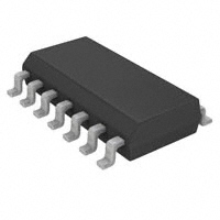
PACKAGE/ORDERING INFORMATION
PRODUCT
PACKAGE
TYPE
PACKAGE
CODE
PACKAGE
MARKING
PCM1801U
14-pin SOIC
D
PCM1801U
ORDERING
NUMBER
TRANSPORT
MEDIA
QUANTITY
PCM1801U
Rails
56
PCM1801U/2K
Tape and reel
2000
ABSOLUTE MAXIMUM RATINGS
Supply voltage: VDD, VCC
–0.3 V to 6.5 V
±0.1 V
Supply voltage differences: VDD, VCC
±0.1 V
GND voltage differences: AGND, DGND
Digital input voltage
–0.3 V to (VDD + 0.3 V), < 6.5 V
Analog input voltage
–0.3 V to (VCC + 0.3 V), < 6.5 V
Input current (any pin except supplies)
±10 mA
Power dissipation
300 mW
Operating temperature range
–25°C to 85°C
Storage temperature
–55°C to 125°C
Lead temperature, soldering
260°C, 5 s
Package temperature (IR reflow, peak)
235°C
RECOMMENDED OPERATING CONDITIONS
over operating free-air temperature range
MIN
NOM
MAX
Analog supply voltage, VCC
4.5
5
5.5
Digital supply voltage, VDD
4.5
5
5.5
Analog input voltage, full-scale (–0 dB)
2.828
Digital input logic family
Digital input clock frequency
V
V
Vp-p
TTL
System clock
Sampling clock
8.192
24.576
MHz
32
48
kHz
Digital output load capacitance
10
Operating free-air temperature, TA
2
UNIT
–25
Submit Documentation Feedback
pF
85
°C
�PCM1801
www.ti.com
SBAS131C – OCTOBER 2000 – REVISED JULY 2007
PIN CONFIGURATION
PCM1801
(TOP VIEW)
VINL
1
14
VREF1
VINR
2
13
VREF2
DGND
3
12
AGND
VDD
4
11
VCC
SCKI
5
10
FMT
BCK
6
9
BYPAS
LRCK
7
8
DOUT
P0005-01
Table 1. PIN ASSIGNMENTS
NAME
PIN
I/O
AGND
12
–
Analog ground
DESCRIPTION
BCK
6
I
Bit clock input
BYPAS
9
I
HPF bypass control (1)
DGND
3
–
Digital ground
DOUT
8
O
Audio data output
FMT
10
I
Audio data format(1)
L: HPF enabled
H: HPF disabled
L: MSB-first, left-justified
H: MSB-first, I2S
(1)
LRCK
7
I
Sampling clock input
SCKI
5
I
System clock input; 256 fS, 384 fS, or 512 fS
VCC
11
–
Analog power supply
VDD
4
–
Digital power supply
VINL
1
I
Analog input, Lch
VINR
2
I
Analog input, Rch
VREF1
14
–
Reference 1 decoupling capacitor
VREF2
13
–
Reference 2 decoupling capacitor
With 100-kΩ typical pulldown resistor
Submit Documentation Feedback
3
�PCM1801
www.ti.com
SBAS131C – OCTOBER 2000 – REVISED JULY 2007
ELECTRICAL CHARACTERISTICS
All specifications at TA = 25°C, VDD = VCC = 5 V, fS = 44.1 kHz, 16-bit data, and SYSCLK = 384 fS, unless otherwise noted.
PARAMETER
TEST CONDITIONS
PCM1801U
MIN
RESOLUTION
TYP
MAX
16
UNITS
Bits
DIGITAL INPUT/OUTPUT
VIH (1)
VIL (1)
IIN (2)
IIN (3)
VOH (4)
VOL
fS
(4)
2
Input logic level
0.8
±10
Input logic current
Output logic level
100
IOH = –1.6 mA
4.5
IOL = 3.2 mA
Sampling frequency
0.5
VDC
μA
VDC
4
44.1
48
256 fS
1.024
11.2896
12.288
384 fS
1.536
16.9344
18.432
512 fS
2.048
22.5792
24.576
±1
±2.5
Gain error
±2
±5
Gain drift
±20
ppm of FSR/°C
System clock frequency
kHz
MHz
DC ACCURACY
Gain mismatch, channel-to-channel
% of FSR
% of FSR
Bipolar zero error
High-pass filter bypassed
±2
% of FSR
Bipolar zero drift
High-pass filter bypassed
±20
ppm of FSR/°C
FS (–0.5 dB)
–88
–60 dB
–90
DYNAMIC PERFORMANCE (5)
THD+N
–80
dB
Dynamic range
A-weighted
90
93
dB
Signal-to-noise ratio
A-weighted
90
93
dB
87
90
dB
2.828
Vp-p
2.1
V
Channel separation
ANALOG INPUT
Input range
FS (VIN = 0 dB)
Center voltage
Input impedance
Antialiasing filter frequency response
–3 dB
30
kΩ
150
kHz
DIGITAL FILTER PERFORMANCE
Pass band
0.454 fS
Stop band
0.583 fS
Hz
±0.05
Pass-band ripple
Stop-band attenuation
–65
Delay time (latency)
High-pass frequency response
(1)
(2)
(3)
(4)
(5)
4
–3 dB
Hz
dB
dB
17.4/fS
s
0.019 fS
mHz
Pins 5, 6, 7, 9, and 10 (SCKI, BCK, LRCK, BYPAS, and FMT)
Pins 5, 6, 7 (SCKI, BCK, LRCK) Schmitt-trigger input
Pins 9, 10 (BYPAS, FMT) Schmitt-trigger input with 100-kΩ typical pulldown resistor
Pin 8 (DOUT)
fIN = 1 kHz, using the System Two™ audio measurement system by Audio Precision™ in rms mode with 20-kHz LPF and 400-Hz HPF
in the performance calculation.
Submit Documentation Feedback
�PCM1801
www.ti.com
SBAS131C – OCTOBER 2000 – REVISED JULY 2007
ELECTRICAL CHARACTERISTICS (continued)
All specifications at TA = 25°C, VDD = VCC = 5 V, fS = 44.1 kHz, 16-bit data, and SYSCLK = 384 fS, unless otherwise noted.
PARAMETER
PCM1801U
TEST CONDITIONS
MIN
TYP
MAX
4.5
5
5.5
4.5
5
5.5
UNITS
POWER SUPPLY REQUIREMENTS
VCC
Voltage range
VDD
VDC
Supply current (6)
VCC = VDD = 5 V
18
24
mA
Power dissipation
VCC = VDD = 5 V
90
120
mW
°C
TEMPERATURE RANGE
TA
Operation
–25
85
Tstg
Storage
–55
125
θJA
Thermal resistance
(6)
°C
°C/W
100
No load on DOUT (pin 8)
BLOCK DIAGRAM
PCM1801
(+)
VINL
Single-End/
Differential
Converter
(−)
5th Order
Delta-Sigma
Modulator
BCK
×1/64
Decimation
and
High-Pass
Filter
VREF1
Reference
VREF2
(−)
VINR
Single-End/
Differential
Converter
(+)
5th Order
Delta-Sigma
Modulator
Serial Data
Interface
LRCK
DOUT
Format
Control
FMT
BYPAS
Clock/Timing Control
SCKI
Power Supply
VCC
AGND DGND
VDD
B0004-02
Submit Documentation Feedback
5
�PCM1801
www.ti.com
SBAS131C – OCTOBER 2000 – REVISED JULY 2007
ANALOG FRONT-END (Single Channel)
1 µF
+
VINL
1
30 kΩ
−
−
1 kΩ
(+)
+
+
1 kΩ
14
4.7 µF
(−)
Delta-Sigma
Modulator
VREF1
+
VREF
4.7 µF
+
13
VREF2
S0011-02
TYPICAL PERFORMANCE CURVES
All specifications at TA = 25°C, VDD = VCC = 5 V, fS = 44.1 kHz, and SYSCLK = 384 fS, unless otherwise noted
ANALOG DYNAMIC PERFORMANCE
3.0
0.005
2.8
−60 dB
0.004
2.6
−0.5 dB
0.003
0.002
−25
2.4
0
25
50
75
TA − Free-Air Temperature − °C
96
96
95
95
94
G001
Figure 1.
6
SNR
93
92
−25
2.2
100
0
93
25
50
75
TA − Free-Air Temperature − °C
Figure 2.
Submit Documentation Feedback
94
Dynamic Range
SNR − Signal-to-Noise Ratio − dB
0.006
Dynamic Range − dB
DYNAMIC RANGE AND SIGNAL-TO-NOISE RATIO
vs
TEMPERATURE
THD+N − Total Harm. Dist. + Noise at −60 dB − %
THD+N − Total Harm. Dist. + Noise at −0.5 dB − %
TOTAL HARMONIC DISTORTION + NOISE
vs
TEMPERATURE
92
100
G002
�PCM1801
www.ti.com
SBAS131C – OCTOBER 2000 – REVISED JULY 2007
TYPICAL PERFORMANCE CURVES (continued)
All specifications at TA = 25°C, VDD = VCC = 5 V, fS = 44.1 kHz, and SYSCLK = 384 fS, unless otherwise noted
0.004
2.6
0.003
2.4
−0.5 dB
4.50
4.75
5.00
5.25
5.50
THD+N − Total Harm. Dist. + Noise at −0.5 dB − %
95
Dynamic Range
94
94
SNR
92
4.25
2.2
5.75
VCC − Supply Voltage − V
95
93
4.50
4.75
93
5.00
5.25
5.50
92
5.75
VCC − Supply Voltage − V
G003
G004
Figure 3.
Figure 4.
TOTAL HARMONIC DISTORTION + NOISE
vs
SAMPLING RATE
DYNAMIC RANGE AND SIGNAL-TO-NOISE RATIO
vs
SAMPLING RATE
0.006
3.0
2.8
0.005
−60 dB
0.004
2.6
0.003
2.4
−0.5 dB
0.002
2.2
32
44.1
Dynamic Range − dB
0.002
4.25
96
96
96
95
95
94
94
Dynamic Range
93
93
SNR
92
48
92
32
Sampling Rate − kHz
G005
Figure 5.
SNR − Signal-to-Noise Ratio − dB
−60 dB
96
SNR − Signal-to-Noise Ratio − dB
2.8
0.005
Dynamic Range − dB
3.0
THD+N − Total Harm. Dist. + Noise at −60 dB − %
0.006
DYNAMIC RANGE AND SIGNAL-TO-NOISE RATIO
vs
SUPPLY VOLTAGE
THD+N − Total Harm. Dist. + Noise at −60 dB − %
THD+N − Total Harm. Dist. + Noise at −0.5 dB − %
TOTAL HARMONIC DISTORTION + NOISE
vs
SUPPLY VOLTAGE
44.1
48
Sampling Rate − kHz
G006
Figure 6.
Submit Documentation Feedback
7
�PCM1801
www.ti.com
SBAS131C – OCTOBER 2000 – REVISED JULY 2007
TYPICAL PERFORMANCE CURVES (continued)
All specifications at TA = 25°C, VDD = VCC = 5 V, fS = 44.1 kHz, and SYSCLK = 384 fS, unless otherwise noted
SUPPLY CURRENT
SUPPLY CURRENT
vs
TEMPERATURE
SUPPLY CURRENT
vs
SUPPLY VOLTAGE
20
20
ICC + IDD
12
ICC
8
IDD
12
ICC
8
IDD
4
0
−25
ICC + IDD
16
ICC − Supply Current − mA
ICC − Supply Current − mA
16
4
0
25
50
75
0
4.25
100
TA − Free-Air Temperature − °C
4.50
4.75
G007
Figure 7.
Figure 8.
SUPPLY CURRENT
vs
SAMPLING RATE
20
ICC + IDD
ICC − Supply Current − mA
16
ICC
12
8
IDD
4
0
0
10
20
30
40
50
Sampling Rate − kHz
G009
Figure 9.
8
5.00
5.25
VCC − Supply Voltage − V
Submit Documentation Feedback
5.50
5.75
G008
�PCM1801
www.ti.com
SBAS131C – OCTOBER 2000 – REVISED JULY 2007
TYPICAL PERFORMANCE CURVES (continued)
All specifications at TA = 25°C, VDD = VCC = 5 V, fS = 44.1 kHz, and SYSCLK = 384 fS, unless otherwise noted
OUTPUT SPECTRUM
–60 dBFS FFT
0
−20
−20
−40
−40
Amplitude − dB
Amplitude − dB
FULL-SCALE FFT
0
−60
−80
−60
−80
−100
−100
−120
−120
−140
−140
0
5
10
15
20
0
5
f − Frequency − kHz
10
15
20
f − Frequency − kHz
G010
G011
Figure 10.
Figure 11.
TOTAL HARMONIC DISTORTION + NOISE
vs
AMPLITUDE
TOTAL HARMONIC DISTORTION + NOISE
vs
FREQUENCY
0.1
THD+N − Total Harmonic Distortion + Noise − %
THD+N − Total Harmonic Distortion + Noise − %
100
10
1
0.1
0.01
0.001
−100
−80
−60
−40
−20
0.01
0.001
0.0001
20
0
Amplitude − dBV
100
1k
10k 20k
f − Frequency − Hz
G012
Figure 12.
G013
Figure 13.
Submit Documentation Feedback
9
�PCM1801
www.ti.com
SBAS131C – OCTOBER 2000 – REVISED JULY 2007
TYPICAL PERFORMANCE CURVES (continued)
All specifications at TA = 25°C, VDD = VCC = 5 V, fS = 44.1 kHz, and SYSCLK = 384 fS, unless otherwise noted
DECIMATION FILTER
OVERALL CHARACTERISTICS
STOP-BAND ATTENUATION CHARACTERISTICS
0
0
−20
Amplitude − dB
Amplitude − dB
−50
−100
−40
−60
−150
−80
−200
0
8
16
24
−100
0.00
32
Normalized Frequency [× fS Hz]
0.25
0.50
0.75
Normalized Frequency [× fS Hz]
G014
Figure 14.
Figure 15.
PASS-BAND RIPPLE CHARACTERISTICS
TRANSITION BAND CHARACTERISTICS
0.2
1.00
G015
0
−1
−2
−3
−0.2
Amplitude − dB
Amplitude − dB
0.0
−0.4
−0.6
−4
−5
−6
−7
−8
−0.8
−9
−1.0
0.0
0.1
0.2
0.3
0.4
Normalized Frequency [× fS Hz]
0.5
−4.13 dB at 0.5 fS
−10
0.45
0.47
0.49
G016
Figure 16.
10
0.51
Normalized Frequency [× fS Hz]
Figure 17.
Submit Documentation Feedback
0.53
0.55
G017
�PCM1801
www.ti.com
SBAS131C – OCTOBER 2000 – REVISED JULY 2007
TYPICAL PERFORMANCE CURVES (continued)
All specifications at TA = 25°C, VDD = VCC = 5 V, fS = 44.1 kHz, and SYSCLK = 384 fS, unless otherwise noted
HIGH-PASS FILTER
HIGH-PASS FILTER RESPONSE
HIGH-PASS FILTER RESPONSE
0.2
0
−10
0.0
−20
Amplitude − dB
Amplitude − dB
−30
−40
−50
−60
−70
−80
−0.2
−0.4
−0.6
−0.8
−90
−100
0.00 0.05 0.10
0.15 0.20 0.25
−1.0
0.0
0.30 0.35 0.40
Normalized Frequency [× fS/1000 Hz]
0.5
1.0
1.5
2.0
2.5
3.0
3.5
Normalized Frequency [× fS/1000 Hz]
G018
Figure 18.
4.0
G019
Figure 19.
ANTIALIASING FILTER
ANTIALIASING FILTER
STOP-BAND CHARACTERISTICS
ANTIALIASING FILTER
PASS-BAND CHARACTERISTICS
0.2
0
0.0
Amplitude − dB
Amplitude − dB
−10
−20
−30
−40
−0.2
−0.4
−0.6
−0.8
−50
−1.0
1
10
100
1k
10k
100k
1M
10M
1
f − Frequency − Hz
10
100
1k
10k
100k
f − Frequency − Hz
G020
Figure 20.
G021
Figure 21.
Submit Documentation Feedback
11
�PCM1801
www.ti.com
SBAS131C – OCTOBER 2000 – REVISED JULY 2007
THEORY OF OPERATION
The PCM1801 consists of a band-gap reference, two channels of a single-to-differential converter, a fully
differential 5th-order delta-sigma modulator, a decimation filter (including digital high-pass), and a serial interface
circuit. The block diagram illustrates the total architecture of the PCM1801, and the analog front-end diagram
illustrates the architecture of the single-to-differential converter and the antialiasing filter. Figure 22 illustrates the
architecture of the 5th-order delta-sigma modulator and transfer functions.
An internal high-precision reference with two external capacitors provides all reference voltages which are
required by the converter, and defines the full-scale voltage range of both channels. The internal single-ended to
differential voltage converter saves the design, space, and extra parts needed for external circuitry required by
many delta-sigma converters. The internal full-differential architecture provides a wide dynamic range and
excellent power-supply rejection performance.
The input signal is sampled at a 64× oversampling rate, eliminating the need for a sample-and-hold circuit and
simplifying antialias filtering requirements. The 5th-order delta-sigma noise shaper consists of five integrators
which use a switched-capacitor topology, a comparator, and a feedback loop consisting of a 1-bit
digital-to-analog converter (DAC). The delta-sigma modulator shapes the quantization noise, shifting it out of the
audio band in the frequency domain. The high order of the modulator enables it to randomize the modulator
outputs, reducing idle tone levels.
The 64-fS, 1-bit stream from the modulator is converted to 1-fS, 16-bit digital data by the decimation filter, which
also acts as a low-pass filter to remove the shaped quantization noise. The dc components are removed by a
digital high-pass filter, and the filtered output is converted to time-multiplexed serial signals through a serial
interface which provides flexible serial formats.
Analog
In
X(z) +
−
1st
SW-CAP
Integrator
+
−
2nd
SW-CAP
Integrator
3rd
SW-CAP
Integrator
+
+
+
+
−
4th
SW-CAP
Integrator
+
+
H(z)
5th
SW-CAP
Integrator
+
+
Qn(z)
Digital
Out
Y(z)
+
Comparator
1-Bit
DAC
Y(z) = STF(z) * X(z) + NTF(z) * Qn(z)
Signal Transfer Function
STF(z) = H(z) / [1 + H(z)]
Noise Transfer Function
NTF(z) = 1 / [1 + H(z)]
B0005-01
Figure 22. Simplified Diagram of the PCM1801 5th-Order Delta-Sigma Modulator
SYSTEM CLOCK
The system clock for the PCM1801 must be either 256 fS, 384 fS, or 512 fS, where fS is the audio sampling
frequency. The system clock must be supplied on SCKI (pin 5).
The PCM1801 also has a system clock detection circuit that automatically senses if the system clock is
operating at 256 fS, 384 fS, or 512 fS.
When a 384-fS or 512-fS system clock is used, the PCM1801 automatically divides the clock down to 256 fS
internally. This 256-fS clock is used to operate the digital filter and the modulator. Table 2 lists the relationship of
typical sampling frequencies and system clock frequencies. Figure 23 illustrates the system clock timing.
12
Submit Documentation Feedback
�PCM1801
www.ti.com
SBAS131C – OCTOBER 2000 – REVISED JULY 2007
Table 2. System Clock Frequencies
SAMPLING RATE FREQUENCY
(kHz)
SYSTEM CLOCK FREQUENCY
256 fs
384 fs
512 fs
32
8.1920
12.2880
16.3840
44.1
11.2896
16.9344
22.5792
48
12.2880
18.4320
24.5760
tCLKIH
tCLKIL
2V
SCKI
0.8 V
T0005-04
System clock pulse duration, HIGH
t(CLKIH)
12 ns (min)
System clock pulse duration, LOW
t(CLKIL)
12 ns (min)
Figure 23. System Clock Timing
POWER-ON RESET
The PCM1801 has an internal power-on reset circuit, which initializes (resets) when the supply voltage
(VCC/VDD) exceeds 4 V (typical). Because the system clock is used as the clock signal for the reset circuit, the
system clock must be supplied as soon as power is applied; more specifically, the device must receive at least
three system clock cycles before VDD > 4 V. While VCC/VDD < 4 V (typical) and for 1024 system clock cycles after
VCC/VDD > 4 V, the PCM1801 stays in the reset state and the digital output is forced to zero. The digital output is
valid 18,436 fS periods after release from the reset state. Figure 24 illustrates the internal power-on reset timing
and the digital output for power-on reset.
VCC / VDD
4.4 V
4V
3.6 V
Reset
Reset Removal
Internal Reset
3 Clocks Minimum
1024 System Clocks
18436 / fS
System Clock
DOUT
Zero Data
Normal Data(1)
T0014-02
(1)
The transient response (exponentially attenuated signal from ±0.2% dc of FSR with a 200-ms time constant) appears
initially.
Figure 24. Internal Power-On Reset Timing
Submit Documentation Feedback
13
�PCM1801
www.ti.com
SBAS131C – OCTOBER 2000 – REVISED JULY 2007
SERIAL AUDIO DATA INTERFACE
The PCM1801 interfaces the audio system through BCK (pin 6), LRCK (pin 7), and DOUT (pin 8).
The PCM1801 accepts 64-BCK/LRCK, 48-BCK/LRCK (only for a 384-fS system clock) or 32-BCK/LRCK format
for the left-justified format. And the PCM1801 accepts the 64-BCK/LRCK or 48-BCK/LRCK format (only for a
384-fS system clock) for I2S format.
DATA FORMAT
The PCM1801 supports two audio data formats in slave mode, which are selected by the FMT control input
(pin 10) as shown in Table 3. Figure 25 illustrates the data format. If the application system cannot ensure an
effective system clock prior to power up of the PCM1801, the FMT pin must be held LOW until the power-on
reset sequence is completed. In this case, if the I2S format (FMT = HIGH) is required in the application, FMT can
be set HIGH after the power-on reset sequence is completed.
Table 3. Data Format
FMT
DATA FORMAT
0 (L)
16-bit, left-justified
1 (H)
16-bit, I2S
FMT = L
16-Bit, MSB-First, Left-Justified
Left-Channel
LRCK
Right-Channel
BCK
DOUT
1
2
3
14 15 16
MSB
1
LSB
2
3
1
14 15 16
MSB
LSB
FMT = H
16-Bit, MSB-First, I2S
LRCK
Left-Channel
Right-Channel
BCK
DOUT
1
2
MSB
3
14 15 16
LSB
1
2
3
MSB
14 15 16
LSB
T0016-03
Figure 25. Audio Data Format
14
Submit Documentation Feedback
�PCM1801
www.ti.com
SBAS131C – OCTOBER 2000 – REVISED JULY 2007
INTERFACE TIMING
Figure 26 illustrates the interface timing.
t(LRCP)
1.4 V
LRCK
t(BCKL)
t(LRSU)
t(BCKH)
t(LRHD)
1.4 V
BCK
t(CKDO)
t(BCKP)
t(LRDO)
0.5 VDD
DOUT
T0017-02
SYMBOL
MIN
BCK period
DESCRIPTION
t(BCKP)
300
TYP
MAX
UNITS
ns
BCK pulse duration, HIGH
t(BCKH)
120
ns
BCK pulse duration, LOW
t(BCKL)
120
ns
LRCK setup time to BCK rising edge
t(LRSU)
80
ns
LRCK hold time to BCK rising edge
t(LRHD)
40
ns
μs
LRCK period
t(LRCP)
20
Delay time, BCK falling edge to DOUT valid
t(CKDO)
–20
40
ns
Delay time, LRCK edge to DOUT valid
t(LRDO)
–20
40
ns
Rising time of all signals
t(RISE)
20
ns
Falling time of all signals
t(FALL)
20
ns
NOTE: Timing measurement reference level is (VIH + VIL)/2. Rising and falling time is
measured from 10% to 90% of the I/O signal swing. Load capacitance of the DOUT
signal is 20 pF.
Figure 26. Audio Data Interface Timing
SYNCHRONIZATION WITH DIGITAL AUDIO SYSTEM
The PCM1801 operates with LRCK synchronized to the system clock (SCKI). The PCM1801 does not require a
specific phase relationship between LRCK and SCKI, but does require the synchronization of LRCK and SCKI. If
the relationship between LRCK and SCKI changes more than 6 bit clocks (BCK) during one sample period due
to LRCK or SCKI jitter, internal operation of the ADC halts within 1/fS and the digital output is forced to BPZ until
resynchronization between LRCK and SCKI is completed. In case of changes less than 5 bit clocks (BCK),
resynchronization does not occur and the previously described digital output control and discontinuity do not
occur. Figure 27 illustrates the ADC digital output for lost synchronization and resynchronization. During
undefined data, some noise may be generated in the audio signal. Also, the transition of normal to undefined
data and undefined or zero data to normal makes a discontinuity of data on the digital output and may generate
some noise in the audio signal.
Submit Documentation Feedback
15
�PCM1801
www.ti.com
SBAS131C – OCTOBER 2000 – REVISED JULY 2007
Synchronization Lost
State of Synchronization
Synchronous
Resynchronization
Asynchronous
Synchronous
1/fS
DOUT
Normal Data
Undefined
Data
32/fS
Zero Data
Normal Data(1)
T0020-02
(1)
The transient response (exponentially attenuated signal from ±0.2% dc of FSR with 200-ms time constant) appears
initially.
Figure 27. ADC Digital Output for Loss of Synchronization and Re-Synchronization
HPF Bypass Control
The built-in function for dc component rejection can be bypassed by BYPAS (pin 9) control (see Table 4). In
bypass mode, the dc component of the input analog signal, the internal dc offset, etc., are also converted and
output in the digital output data.
Table 4. HPF Bypass Control
BYPAS
HIGH-PASS FILTER (HPF) MODE
Low
Normal (dc cut) mode
High
Bypass (through) mode
APPLICATION INFORMATION
BOARD DESIGN AND LAYOUT CONSIDERATIONS
VCC, VDD PINS
The digital and analog power supply lines to the PCM1801 should be bypassed to the corresponding ground
pins with both 0.1-μF ceramic and 10-μF tantalum capacitors as close to the pins as possible to maximize the
dynamic performance of the ADC. Although the PCM1801 has two power lines to maximize the potential of
dynamic performance, using one common power supply is recommended to avoid unexpected power supply
problems, such as latch-up due to power supply sequencing.
AGND, DGND PINS
To maximize the dynamic performance of the PCM1801, the analog and digital grounds are not internally
connected. These points should have low impedance to avoid digital noise feedback into the analog ground.
They should be connected directly to each other under the PCM1801 package to reduce potential noise
problems.
VIN PINS
A 1.0-μF tantalum capacitor is recommended as an ac-coupling capacitor, which establishes a 5.3-Hz cutoff
frequency. If a higher full-scale input voltage is required, the input voltage range can be increased by adding a
series resistor to the VIN pins.
VREF PINS
To ensure low source impedance, 4.7-μF tantalum capacitors are recommended from VREF1 to AGND and from
VREF2 to AGND. These capacitors should be located as close as possible to the VREF1 and VREF2 pins to reduce
dynamic errors on the ADC references.
16
Submit Documentation Feedback
�PCM1801
www.ti.com
SBAS131C – OCTOBER 2000 – REVISED JULY 2007
APPLICATION INFORMATION (continued)
DOUT PIN
The DOUT pin has a large load-drive capability, but locating a buffer near the PCM1801 and minimizing load
capacitance is recommended in order to minimize the digital-analog crosstalk and maximize the dynamic
performance of the ADC.
FMT PIN
In general, the FMT pin is used for audio data format selection by tying up DGND or VDD in accordance with
interface requirements. If the application system cannot ensure an effective system clock prior to power up of
the PCM1801 when I2S format is required, then the FMT pin must be set HIGH after the power-on reset
sequence. This input control can be accomplished easily by connecting a C-R delay circuit with a delay time
greater than 1 ms to the FMT pin.
SYSTEM CLOCK
The quality of the system clock can influence dynamic performance in the PCM1801. The duty cycle, jitter, and
threshold voltage at the system clock input pin must be carefully managed. When power is supplied to the part,
the system clock, bit clock (BCK), and word clock (LRCK) should also be supplied simultaneously. Failure to
supply the audio clocks results in a power dissipation increase of up to three times normal dissipation and may
degrade long-term reliability if the maximum power dissipation limit is exceeded.
TYPICAL CIRCUIT CONNECTION DIAGRAM
Figure 28 is a typical connection diagram illustrating a circuit for which the input HPF cutoff frequency is about
5 Hz.
Lch In
Rch In
C1(1)
+
C2(1)
+
C3(2)
Audio
Data
Processor
1
VINL
VREF1
14
2
VINR
VREF2
13
3
DGND
AGND
12
+
C6(3)
+
C5(3)
0V
C4(2)
4
VDD
VCC
11
System Clock
5
SCKI
FMT
10
Format
Data Clock
6
BCK
BYPAS
9
Bypass
Latch Enable
7
LRCK
DOUT
8
+5 V
Pin Program
or Control
Data Out
S0013-01
(1)
C1 and C2: A 1-μF capacitor gives a 5.3-Hz (τ = 1 μF * 30 kΩ) cutoff frequency for the input HPF in normal operation
and requires a power-on setting time of 30 ms at power up.
(2)
C3 and C4: Bypass capacitors, 0.1-μF ceramic and 10-μF tantalum or aluminum electrolytic, depending on layout
and power supply
(3)
C5 and C6: 4.7-μF tantalum or aluminum electrolytic capacitors
Figure 28. Typical Circuit Connection
Submit Documentation Feedback
17
�PACKAGE OPTION ADDENDUM
www.ti.com
15-Dec-2022
PACKAGING INFORMATION
Orderable Device
Status
(1)
Package Type Package Pins Package
Drawing
Qty
Eco Plan
(2)
Lead finish/
Ball material
MSL Peak Temp
Op Temp (°C)
Device Marking
(3)
Samples
(4/5)
(6)
PCM1801U
ACTIVE
SOIC
D
14
50
RoHS & Green
NIPDAU
Level-1-260C-UNLIM
-25 to 85
PCM1801U
Samples
PCM1801U/2K
ACTIVE
SOIC
D
14
2000
RoHS & Green
NIPDAU
Level-1-260C-UNLIM
-25 to 85
PCM1801U
Samples
PCM1801U/2KG4
ACTIVE
SOIC
D
14
2000
RoHS & Green
NIPDAU
Level-1-260C-UNLIM
PCM1801U
Samples
(1)
The marketing status values are defined as follows:
ACTIVE: Product device recommended for new designs.
LIFEBUY: TI has announced that the device will be discontinued, and a lifetime-buy period is in effect.
NRND: Not recommended for new designs. Device is in production to support existing customers, but TI does not recommend using this part in a new design.
PREVIEW: Device has been announced but is not in production. Samples may or may not be available.
OBSOLETE: TI has discontinued the production of the device.
(2)
RoHS: TI defines "RoHS" to mean semiconductor products that are compliant with the current EU RoHS requirements for all 10 RoHS substances, including the requirement that RoHS substance
do not exceed 0.1% by weight in homogeneous materials. Where designed to be soldered at high temperatures, "RoHS" products are suitable for use in specified lead-free processes. TI may
reference these types of products as "Pb-Free".
RoHS Exempt: TI defines "RoHS Exempt" to mean products that contain lead but are compliant with EU RoHS pursuant to a specific EU RoHS exemption.
Green: TI defines "Green" to mean the content of Chlorine (Cl) and Bromine (Br) based flame retardants meet JS709B low halogen requirements of