User's Guide
SLAU615 – December 2014
PCM186xEVM
The PCM186xEVM (EVM) is an easy-to-use evaluation board for the PCM186x family of ADCs. This
document details the materials received with the EVM, how to get started with the software and hardware,
the schematics, bill of materials (BOM), and layouts. Throughout this user's guide, the abbreviations EVM,
PCM186xEVM, and the term evaluation module are synonymous with the PCM1860EVM, PCM1861EVM,
PCM1862EVM, PCM1863EVM, PCM1864EVM, or PCM1865EVM, unless otherwise noted.
1
2
3
4
5
6
Contents
Introduction ................................................................................................................... 2
What’s in the Box? ........................................................................................................... 3
2.1
PCM186xEVM....................................................................................................... 3
2.2
USB-I2X board ...................................................................................................... 3
2.3
Micro USB Cable ................................................................................................... 3
Getting Started ............................................................................................................... 4
3.1
System Hardware Overview ....................................................................................... 4
3.2
Block Diagram ....................................................................................................... 5
3.3
Software Download ................................................................................................. 5
Hardware...................................................................................................................... 6
4.1
Power Requirements ............................................................................................... 6
4.2
Connectors and Headers .......................................................................................... 6
4.3
Board Configurations ............................................................................................... 8
4.4
Solder Options ...................................................................................................... 9
Software ..................................................................................................................... 10
5.1
Installation .......................................................................................................... 10
5.2
Navigation and Features ......................................................................................... 12
Schematics, Bill of Materials and Layouts .............................................................................. 15
6.1
Schematics ......................................................................................................... 15
6.2
Bill of Materials .................................................................................................... 17
6.3
Layouts ............................................................................................................. 19
List of Figures
................................................................................................... 3
.................................................................................................. 3
PCM186xEVM Mated to the USB-I2X Board ............................................................................ 4
Block Diagram ................................................................................................................ 5
Diagram of Connector/Header Locations ................................................................................. 6
Mode 0 Block Diagram ..................................................................................................... 8
Mode 1 Block Diagram ...................................................................................................... 8
Mode 2 Block Diagram ...................................................................................................... 9
Solder Options ............................................................................................................... 9
PCM186X EVM GUI ....................................................................................................... 10
Manual Target Selection Window ........................................................................................ 11
EVM Tab .................................................................................................................... 12
Direct I2C Read/Write Tab ................................................................................................. 13
1P-1M Differential and 2P-2M Differential Shown in Block Diagram Tab........................................... 14
1
Picture of PCM186xEVM
2
Picture of USB-I2X Board
3
4
5
6
7
8
9
10
11
12
13
14
PurePath is a trademark of Texas Instruments.
SLAU615 – December 2014
Submit Documentation Feedback
PCM186xEVM
Copyright © 2014, Texas Instruments Incorporated
1
�Introduction
www.ti.com
15
PCM186xEVM Schematic ................................................................................................. 15
16
PCM186xEVM Schematic, SPDIF I/O and Controller Board I/O..................................................... 16
17
Top Silk Screen ............................................................................................................. 19
18
Top copper .................................................................................................................. 19
19
Bottom Copper.............................................................................................................. 20
List of Tables
1
1
Part Differences .............................................................................................................. 2
2
J7 Controls.................................................................................................................... 7
3
Mode Summary .............................................................................................................. 9
4
Bill of Materials for PCM186xEVM ....................................................................................... 17
Introduction
The PCM186xEVM (EVM) is an easy-to-use evaluation board for the PCM186x family of ADCs. Due to
the pin-for-pin nature of the PCM186x family, any of the following part numbers can be used with this
board; PCM1860, PCM1861, PCM1862, PCM1863, PCM1864, and PCM1865. The differences between
these parts are shown in Table 1.
Table 1. Part Differences
Part Number
Register Programmable
Hardware Programmable
Number of ADC Channels
PCM1860
Yes
2
PCM1861
Yes
2
PCM1862
Yes
2
PCM1863
Yes
2
PCM1864
Yes
4
PCM1865
Yes
4
The PCM186xEVM has an external +5-V power connection or USB +5 V through the USB-I2X board to
power the EVM. In conjunction with the USB-I2X board, all of the register programming can be done via
USB. In the case of the hardware-controlled parts, resistors are included to tie inputs high or low. There
are headers and test points for most signals to and from the PCM186x. Digital audio can be streamed
from the included SPDIF optical connectors or though a USB to a PC.
2
PCM186xEVM
SLAU615 – December 2014
Submit Documentation Feedback
Copyright © 2014, Texas Instruments Incorporated
�What’s in the Box?
www.ti.com
2
What’s in the Box?
2.1
PCM186xEVM
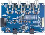
Figure 1 is a photo of the EVM.
Figure 1. Picture of PCM186xEVM
2.2
USB-I2X board
Figure 2 is a photo of the USB-I2X board.
Figure 2. Picture of USB-I2X Board
2.3
Micro USB Cable
A micro USB cable is also included in the box
SLAU615 – December 2014
Submit Documentation Feedback
PCM186xEVM
Copyright © 2014, Texas Instruments Incorporated
3
�Getting Started
www.ti.com
3
Getting Started
3.1
System Hardware Overview
The PCM186xEVM can be controlled though the use of the USB using the included USB-I2X board. The
USB-I2X board connects to a PC via USB and provides digital control signals to the EVM board via I2C.
The USB-I2X board also can supply serial digital audio in and out from the PC to the EVM through an I2S
interface. When connected, the USB-I2X board also supplies all of the power required for the EVM
through USB. The PCM186xEVM also uses a PCM9211 which allows the EVM to receive and transmit
digital audio via optical/SPDIF connectors on the EVM. The PCM9211 converts the optical data to I2S
which can be routed to the PCM186xEVM.
The USB-I2X board mates to the PCM186xEVM as shown in Figure 3.
Figure 3. PCM186xEVM Mated to the USB-I2X Board
4
PCM186xEVM
SLAU615 – December 2014
Submit Documentation Feedback
Copyright © 2014, Texas Instruments Incorporated
�Getting Started
www.ti.com
3.2
Block Diagram
Figure 4 shows a block diagram of the mated boards.
Vin1
Vin2
Vin3
Vin4
PCM186x
I2S
USB
USB-I2X
I2C
PCM9211
SPDIF
SPDIF
Opto In
Opto Out
Figure 4. Block Diagram
The EVM has several different clocking options and can be run in one of three different modes. These
modes also control how the audio data is routed. The default mode is Mode 0, for more detail on the
available modes, refer to Section 4.3.
3.3
Software Download
The EVM is controlled through the PurePath™ Console. Request PurePath Console access here:
www.ti.com/tool/purepathconsole.
Once access is granted, download the PurePath Console here: http://cc.ext.ti.com
SLAU615 – December 2014
Submit Documentation Feedback
PCM186xEVM
Copyright © 2014, Texas Instruments Incorporated
5
�Hardware
www.ti.com
4
Hardware
4.1
Power Requirements
The PCM186xEVM requires a 5-V power supply. This can be sourced from the I2X board via USB or
applied directly to the EVM on the +5-V header just above J1. Once 5 V is applied, the PCM186x board
regulates the 5 V down to a clean analog 3.3 V. A green LED just to the right of the 5-V header illuminates
if the voltages are present.
4.2
Connectors and Headers
Figure 5. Diagram of Connector/Header Locations
•
•
•
•
•
•
•
•
6
J1 – J1 is the I2X board connector. Provides I2C, I2S and +5 V connections to the PCM186x EVM.
+5V – Input for power if no USB-I2X board is used. Output for +5 V, if USB-I2X board is used.
Vin1 – Pins 3 (red-top input) and 4 (white-bottom input) of the PCM186x. AC coupled.
Vin2 – Pins 1 (red-top input) and 2 (white-bottom input) of the PCM186x. AC coupled.
Vin3 – Pins 30 (red-top input) and 29 (white-bottom input) of the PCM186x. AC coupled.
Vin4 – Pins 28 (red-top input) and 27 (white-bottom input) of the PCM186x. AC coupled.
J6 – J6 can be used to insert an external Mic Bias (remove J9).
J7 – Most of the PCM186x GPIO, hardware control, and I2C signals are available here.
PCM186xEVM
SLAU615 – December 2014
Submit Documentation Feedback
Copyright © 2014, Texas Instruments Incorporated
�Hardware
www.ti.com
Table 2. J7 Controls
J7 Pin
•
•
•
•
•
•
•
Description
1
MD0
2
Ground
3
MD1/AD
4
Ground
5
MD3/MC/SCL
6
Ground
7
Dout2/MD2/MOSI/SDA
8
Ground
9
MD4/MISO/GPIO
10
Ground
11
MD5/GPIO1/INTA/DMIN
12
Ground
13
MD6/GPIO2/INTB/DMCLK
14
Ground
15
INT/GPIO3/INTC
16
Ground
J8 – J8 is used to enable or disable the Y0 crystal buffer. With the jumper inserted, this buffer is
disabled. With the jumper removed, the buffer is enabled.
J9 – J9 is used to connect Mic Bias to the inputs for use with an electric microphone. If the jumper is
installed, the Mic Bias is connected to the inputs, if the jumper is removed, Mic Bias is disconnected.
J10 – J10 is used to connect the crystal output (Y0) to a buffer. If the crystal output is being used,
insert J10.
J11 – J11 is used to connect the Xi pin of the PCM186x to ground. If the crystal (Y0) is not used, Xi
should be grounded by inserting a jumper on J11. If the crystal is used, remove the J11 jumper.
Opto Out – Opto out is the SPDIF output of the PCM9211.
Y0 – Y0 is a socked crystal for the PCM186x. If using the PCM186x as the master, insert this crystal. If
the PCM186x is used as a slave, remove the crystal.
Opto In – Opto in is the SPDIF input to the PCM9211. The PCM186x can mix this digital input with
ADC output.
SLAU615 – December 2014
Submit Documentation Feedback
PCM186xEVM
Copyright © 2014, Texas Instruments Incorporated
7
�Hardware
4.3
www.ti.com
Board Configurations
Mode 0 is the default mode after power up (Figure 6). In mode 0, the master clock is supplied from the
PCM9211 and the PCM186x is the slave. Optical inputs are routed to the PCM186x I2S inputs. The
optical input also sets the sample rate of the system to match the optical rate. If no input is provided, the
sample rate is generated by the PCM9211 and is 48 kHz. The I2X board provides I2C control and power
only. In mode 0, Y0 can be removed and jumpers should be placed on J8 and J11.
Vin1
Vin2
Vin3
Vin4
PCM186x
(Slave)
SCKI BCK LRCK
USB
USB-I2X
Din
Dout
SCKO BCK LRCK Dout
Din
I2C
(Master)
PCM9211
SPDIF
SPDIF
Opto In
Opto Out
Figure 6. Mode 0 Block Diagram
In Mode 1, the PCM186x is the master (Figure 7). Clocking is provided by Y0. I2S is sent to the optical
output. The optical input is not available in this mode. The I2X board will provide I2C control and power
only. In mode 1, install Y0 and J10.
Vin1
Vin2
Vin3
Vin4
PCM186x
(Master)
XO
USB
USB-I2X
BCK LRCK Dout
I2C
SCKI BCK LRCK
Din
(Slave)
PCM9211
SPDIF
Opto Out
Figure 7. Mode 1 Block Diagram
8
PCM186xEVM
SLAU615 – December 2014
Submit Documentation Feedback
Copyright © 2014, Texas Instruments Incorporated
�Hardware
www.ti.com
In Mode 2, the I2X board is the master (Figure 8). I2S in and out to the PCM186x is via the I2X board and
is available to a PC via USB. The optical input and output are not available. Remove Y0 and place
jumpers on J8 and J11 to use this mode.
Vin1
Vin2
Vin3
Vin4
PCM186x
(Slave)
SCKI BCK LRCK
USB-I2X
USB
(Master)
Din
Dout
MCLK
BCK
LRCK
Dout
Din
I2C
PCM9211
Figure 8. Mode 2 Block Diagram
Table 3. Mode Summary
4.4
Mode
Function
J8
J10
J11
Crystal Y0
Mode 0
I2S input and output to PCM9211, running
on I2S clocks
Installed
Removed
Installed
Do not care
Mode1
I2S output to PCM9211 running on crystal
Installed
Installed
Removed
Installed
Mode2
I2S input and output to USB running on I2S
clocks
Installed
Removed
Installed
Do not care
Solder Options
The PCM1861 is completely hardware controlled. In addition to the hardware controlled versions of the
PCM186x family, all of the devices have GPIO. In order to accommodate these hardware and GPIO
options, a series of 3-way resistor connections are included on the EVM. Just to the left of J7, there are 8
zero-Ω resistors. By default, they are connected to pass the signals to J7. These resistors can also be
reoriented up to tie these pins high, or down to tie these pins low. For the proper settings of these multifunction pins, see the PCM186x data sheet (SLAS831).
Tied High
Tied Low
Pass to J7
Figure 9. Solder Options
SLAU615 – December 2014
Submit Documentation Feedback
PCM186xEVM
Copyright © 2014, Texas Instruments Incorporated
9
�Software
5
Software
5.1
Installation
www.ti.com
Access to the PurePath™ Console (PPC2) can be requested here: www.ti.com/tool/purepathconsole.
Once access is granted, download the PurePath Console here: http://cc.ext.ti.com.
After downloading the zip file containing the PPC2 release for PCM186X, unzip the contents. Inside the
zip file is an executable to install PPC2 and a .ppc2 file, this is the PCM186X plugin. Save the plugin in a
file to access later, start the PPC2 installation.
Once the installation is complete, start PPC2. Plug in the USB cable connected to the USB-I2X board,
which should be connected to the PCM186X EVM. If the GUI does not automatically load the PCM186X
GUI, you must manually select the plugin.
Figure 10. PCM186X EVM GUI
Select Manually Choose a Target, a menu should appear that will show the list on installed plugins and
the option to add a target.
10
PCM186xEVM
SLAU615 – December 2014
Submit Documentation Feedback
Copyright © 2014, Texas Instruments Incorporated
�Software
www.ti.com
Figure 11. Manual Target Selection Window
If PCM186X does not appear in the list, select Add Target. Find the PCM186X plugin that was previously
downloaded.
SLAU615 – December 2014
Submit Documentation Feedback
PCM186xEVM
Copyright © 2014, Texas Instruments Incorporated
11
�Software
5.2
www.ti.com
Navigation and Features
After the plugin is loaded and the device has been connected, the first window should look like Figure 12.
The mode can be changed by the drop down menu on the right.
Figure 12. EVM Tab
One very useful feature of the PurePath Console is the ability to load, save, and run scripts. Scripts are
text files that include each I2C write that is going to be sent to the PCM186x. Although the GUI is useful
for making rapid changes and experiments, the goal is developing a script that can be run and saved.
To access the script editing area, click on the Direct I2C Read/Write tab.
12
PCM186xEVM
SLAU615 – December 2014
Submit Documentation Feedback
Copyright © 2014, Texas Instruments Incorporated
�Software
www.ti.com
Figure 13. Direct I2C Read/Write Tab
By clicking on the Load button in the right window, any script.txt file can be opened. Editing, saving and
running the script from this window is also possible.
In the default setting, to get audio out from the EVM quickly, connect a left and right analog audio signal
into Vin1, and connect a system that accepts digital audio through the optical out. To improve
performance, supply a differential audio signal to the part and select 1P-1M Differential and 2P-2M
Differential in the Block Diagram tab.
SLAU615 – December 2014
Submit Documentation Feedback
PCM186xEVM
Copyright © 2014, Texas Instruments Incorporated
13
�Software
www.ti.com
Figure 14. 1P-1M Differential and 2P-2M Differential Shown in Block Diagram Tab
14
PCM186xEVM
SLAU615 – December 2014
Submit Documentation Feedback
Copyright © 2014, Texas Instruments Incorporated
�Schematics, Bill of Materials and Layouts
www.ti.com
6
Schematics, Bill of Materials and Layouts
6.1
Schematics
Figure 15 and Figure 16 are the schematics for the PCM186xEVM.
PCM186xDBT EVALUATION BOARD
ANALOG
INPUTS
IN2L
1
J2
DNP
2
GND
IN2R
R4
3
100LS
VIN2
10uF/16V
2
R
10uF/16V
GND
R40
R41
100K
0402
100K
0402
GND
GND
IN1L
1
GND
IN1R
GND
100K
0402
100K
0402
GND
GND
24.576MHz
HC-49USX
GND
2
GND
C3
2L
Orange
VINR4/VIN3M
100LS
3R
2
J9
4R
+3.3VA
Orange
3
1
30
2
29
3
28
4
27
5
26
3
C19
C40
0.1ufd/16V
0402 X7R
0.1ufd/16V
0402 X7R
GND
+3.3V
U4
6
1
5
2
4
100LS
VCCB
OE
B
VCCA
GND
A
1
J10
2
3
100LS
R2
GND
0.1ufd/16V
0402 X7R
GND
GND
C10
C11
1.0ufd/16V
0603 X7R
0.1ufd/16V
0402 X7R
+1.8V
2
0.0
0603
SCKI
Orange
GND
GND
C12
10ufd/10V
0805 X7R
C13
0.1ufd/16V
0402 X7R
1
R46
R47
100K
0402
100K
0402
GND
GND
GND
L
R
VIN4
Case
GND
MD0
2
1
GND
MD1/AD
GND
3
7
24
MD3/MC/SCL
8
23
DOUT2/MD2/MOSI/SDA
9
22
MD4/MISO/GPIO
10
21
MD5/GPIO1/INTA/DMIN
3
11
20
MD6/GPIO2/INTB/DMCLK
19
INT/GPIO3/INTC
18
14
17
15
16
1
SDA-PCM
2
4 0603
3
MD4/MISO/GPIO
2
4 0603
3
DOUT
Orange
1
GND
MD5/GPIO1/INTA/DMIN
J7
1
2
3
4
5
6
7
8
9
10
11
12
13
14
15
16
GND
2
4 0603
BCK
+3.3VA
GND
Orange
3
Orange
LRCK
+3.3VA
3
1
MD6/GPIO2/INTB/DMCLK
2
GPIO
SETTINGS
GND
INT/GPIO3/INTC
2
4 0603
TSSOP30-DBT
R21 R22
1
4 0603
Orange
0.0
0603
1
+3.3VA
DIN
0.0
0603
SCL-PCM
GND
DOUT2/MD2/MOSI/SDA
GND
12
0.0
0603
2
+3.3VA
13
R20
MD3/MC/SCL
+3.3VA
MD1/AD
PCM1860DBT
PCM1861DBT
PCM1862DBT
PCM1863DBT
PCM1864DBT
PCM1865DBT
1
4 0603
MD0
25
R3
GPIO
I2C
2
+3.3VA
GND
GND
XO-BUF
SCKI
LRCK
BCK
DIN
C9
1
GND
+3.3VA
SPDIF I2S
C8
10ufd/10V
0805 X7R
+1.8V
TXB0101DBV
SOT23-DBV6
GND
R1
0.0
0603
GND
+3.3V
4.99K
0402
+3.3VA
GND
4 0603
6
0603 X7R
GND
GND
GND
VIN3
Case
+3.3VA
1
+1.8V
100K
0402
4 0603
0603 COG
+3.3V
R45
100K
0402
2
Orange
U1
C5
R44
1
0805 X7R
Orange
XI
R
0805 X7R
4L
XO
1.0ufd/16V
GND
IN4R
3L
100LS
0603 COG
GND
IN4L
2
C18
10uF/16V
Orange
1
1L
VINL4/VIN4M
L
2
100LS
C17
10uF/16V
GND
2R
Orange
1
3
1R
100LS
I2C BUS
0805 X7R
J5
J6
1
0805 X7R
C14
1
2
GND
IN3R
3
C16
GND
VINR1/VIN2P
0805 X7R
2
ANALOG
INPUTS
100LS
0.1ufd/50V
0603 X7R
VINL1/VIN1P
0805 X7R
DEFAULT: SMD0805 10uF/16V/X7R
ALT: VSA-10uF/16V/ELECTROLYTIC
J11
J4
IN3L
C15
10uF/16V
Orange
100LS
2
J8
DUAL FOOTPRINT
DEFAULT: SMD0805 10uF/16V/X7R
ALT: VSA-10uF/16V/ELECTROLYTIC
VINL3/VIN4P
3
XI
R13
2.20K
0603
Orange
C7
20pfd/50V
R11
2.20K
0603
10uF/16V
DUAL FOOTPRINT
C6
20pfd/50V
R10
2.20K
0603
0805 X7R
Orange
1
R9
VINR3/VIN3P
PIN HEADER SOCKET
FOR CRYSTAL
XO
Y0
2.20K
0603
VINR2/VIN2M
C4
R43
R8
2.20K
0603
MICBIAS
10uF/16V
R42
R7
MICBIAS
2
Case
2.20K
0603
J3
10uF/16V
R
R6
2.20K
0603
2
1
L
R5
2.20K
0603
VINL2/VIN1M
0805 X7R
C2
Case
VIN1
C1
1
L
1
R12
649
0603
1-3:Pullup
3-4:PullDown
3-2: Bypass
LED
Green/2.1V
0603
0.0
0603
GND
SCKI
LRCK
DOUT
DOUT
BCK
DIN
SPDIF I2S
SDA-PCM
SCL-PCM
TI
PAGE INFO:
PCM186xDBT EVALUATION BOARD SCHEMATIC
DESIGN LEAD DAVID K. WILSON
DATE
NOVEMBER 12, 2013
FILENAME PCM186xEVM_RevC.sbk
SCH REV
C
PCB REV
C
SHEET 1
OF 4
DRAWN BY
LDN
Figure 15. PCM186xEVM Schematic
SLAU615 – December 2014
Submit Documentation Feedback
PCM186xEVM
Copyright © 2014, Texas Instruments Incorporated
15
�Schematics, Bill of Materials and Layouts
www.ti.com
PCM186xDBT EVALUATION BOARD
OPTICAL SPDIF IN
OPTO-IN
1
+3.3V
2
C36
0.1ufd/16V
0402 X7R
VCC
SCL-PCM
GND
GND
OUT
Case
SPDIF
PLR135/T10
GND
GND
MOUNTING HARDWARE
SDA-PCM
SPDIF-IN
3
R28
R29
R35
4.99K
0402
0.0
0603
0.0
0603
GND
+3.3V
Green/2.1V
0603
1.00K
0402
357
0603
27pfd/50V
0402 COG
C39
C25
10ufd/10V
0603 X5R
GND
25
26
28
27
30
29
32
31
34
33
36
0.1ufd/16V
0402 X7R
+5V
U3
19
BCK
PCM9211PT
18
LRCK
17
DIN
4700pfd/25V
0402 X7R
R27
I2C Add = 0x80
C27
C35
10ufd/10V
0603 X5R
0.1ufd/16V
0402 X7R
GND
GND
VCC
GND
46
15
47
14
SPDIF-OUT
1
R37
INPUT
+3.3V
3
GND
SHIELD
PLT133/T10W
13
GND
GND
INV1
GND
1
PCM186x
5
2
XO-BUF
XO-BUF
BCK
LRCK
DOUT
XO-BUF
R18
0.0 5%
BCK
+3.3V
LOCK
3
4
SCKI
0402
GND
LRCK
SN74LVC1G14DRL
SOT553-DRL5
Blue/2.9V
0402
R38
360
0402
GND
+3.3V
DOUT
C24
0.1ufd/16V
0402 X7R
R19
J1
2
10.0K
0603
1
100LS
OPTO-OUT
GND
16
48
C29
OPTICAL SPDIF OUT
0.1ufd/16V
0402 X7R
GND
VOUT
0.068ufd/50V
0402 X7R
+3.3V
C23
LQFP48-PT
44
C28
1
2
GND
GND
680
0402
GND
10ufd/10V
0603 X5R
GND
43
45
GND
C22
SCKI
42
C26
11
GND
0.1ufd/16V
0402 X7R
12
SOT230DBV5
3.3V/400mA
GND
1.0
0603
9
TPS73633DBVT
GND
+3.3V
10
1.0ufd/10V
0402 X5R
20
7
C34
10ufd/10V
0603 X5R
41
8
C33
4
21
5
GND
3
22
40
C21
GND
5
2
39
6
0.1ufd/16V
0402 X7R
+3.3V
GND
4.99K
0402
GND
+3.3VA
VR1
1
M3
R36
GND
R26
POWER SUPPLY AND DECOUPLING
+5V
C32
23
3
GND
Y1
24.576 MHz
ABM10
27pfd/50V
0402 COG
10ufd/10V
0603 X5R
24
38
4
0.1ufd/16V
0402 X7R
C31
37
R34
GND
M3
M3
STANDOFFS WASHERS SCREWS
GND
C38
2
C37
M3
GND
0.1ufd/16V
0402 X7R
3.3V
R25
GND
RESET
C20
35
SPDIF RESET
GND
M3x8 M3x8 M3x8 M3x8
+3.3V
+3.3VA
GND
M3x12 M3x12 M3x12 M3x12
+3.3V +5V
GND
SPDIF
LOCK
LED
0.0 5%
0402
1
2
PCM186x
3
4
5
USB-I2X
CONTROLLER
BOARD
6
GND
I2X-LRCLK
7
8
I2X-SDIN
I2C
SCKI
DIN
I2S
9
10
+3.3V
I2X-SCLK
11
12
I2X-SDOUT
13
14
I2X-MCLK
15
SDA
16
SCL
8
10.0K
0402
2
7
R31
3
6
SCL
4
5
SDA
10.0K
0402
R32
+3.3V
10.0K
0402
PAGE INFO:
SPDIF I/O, CONTROLLER BOARD I/O
DESIGN LEAD DAVID K. WILSON
1.0ufd/10V
0402 X5R
1
GND
0.10"
C30
GND
U2
R30
+3.3V
TI
SCL-PCM
SDA-PCM
24LC256-I/MS
GND
MSOP8-MS
R23
R24
0.0
0603
0.0
0603
SCL
Orange
SCL
SDA
SDA
R33
Orange
GND
10.0K
0402
DATE
NOVEMBER 12, 2013
FILENAME PCM186xEVM_RevC.sbk
SCH REV
C
PCB REV
C
SHEET 2 OF 4
DRAWN BY
LDN
Figure 16. PCM186xEVM Schematic, SPDIF I/O and Controller Board I/O
16
PCM186xEVM
SLAU615 – December 2014
Submit Documentation Feedback
Copyright © 2014, Texas Instruments Incorporated
�Schematics, Bill of Materials and Layouts
www.ti.com
6.2
Bill of Materials
Table 4 lists the PCM186xEVM BOM.
Table 4. Bill of Materials for PCM186xEVM
Item
MANU PART NUM
MANU
REF DES
Description
1
PCM1865DBT
TEXAS INSTRUMENTS
Qty
1
U1
MIC TO 2VRMS ANALOG IN 24-BIT 192 kHz STEREO FRONT END TSSOP30-DBT ROHS
2
24LC256-I/MS
MICROCHIP
1
U2
SERIAL EEPROM I2C 256K 400kHz MSOP8-MS ROHS
3
PCM9211PTR
TEXAS INSTRUMENTS
1
U3
192kHz DIG AUDIO INTERFACE TRANSCEIVER W/STEREO ADC AND ROUTING LQFP48PT ROHS
4
TXB0101DBVR
TEXAS INSTRUMENTS
1
U4
1-BIT BIDIR LEVEL TRANSLATOR SOT23-DBV6 ROHS
5
SN74LVC1G14DRLR
TEXAS INSTRUMENTS
1
INV1
SINGLE INVERTER GATE SCHMITT-TRIGGER SOT553-DRL5 ROHS
6
TPS73633DBVT
TEXAS INSTRUMENTS
1
VR1
VOLT REG 3.3V 400MA LDO CAP FREE NMOS SOT23-DBV5 ROHS
7
PLR135/T10
EVERLIGHT ELECTRONICS
1
OPTO-IN
PHOTOLINK FIBER OPTIC RECEIVER 2.4-5.5V 15MB PCB-RA SHUTTER ROHS
8
PLT133/T10W
EVERLIGHT ELECTRONICS
1
OPTO-OUT
PHOTOLINK FIBER OPTIC TRANSMITTER 2.4-5.5V 15MB PCB-RA SHUTTER ROHS
9
LTST-C190GKT
LITE-ON INC.
2
LED, 3.3V
LED GREEN SMD0603 2.1V 10mA ROHS
10
SMLP12BC7TT86
ROHM SEMICONDUCTOR
1
LOCK
LED BLUE SMD0402 2.9V 10mA ROHS
11
ABM10-24.576MHZ-E20-T
ABRACON
1
Y1
CRYSTAL SMT-ABM10 24.576MHz 4 PIN 10PFD FUNDAMENTAL ROHS
12
EMK212BB7106MG-T
TAIYO YUDEN
8
C1–C4, C15, C16, C17, C18
CAP SMD0805 CERM 10uF 16V 20% X7R ROHS
13
C1608X7R1C105K
TDK
2
C5, C10
CAP SMD0603 CERM 1.0UFD 16V 10% X7R ROHS
14
GRM1885C1H200JA01D
MURATA
2
C6, C7
CAP SMD0603 CERM 20PFD 50V 5% COG ROHS
15
GRM21BR71A106KE51L
MURATA
2
C8, C12
CAP SMD0805 CERM 10UFD 10V10% X7R ROHS
16
GRM155R71C104KA88D
MURATA
14
C9, C11, C13, C19, C20, C21,
C23, C24, C26, C32, C35–C37,
C40
CAP SMD0402 CERM 0.1UFD 16V X7R 10% ROHS
17
GRM188R71H104KA93D
MURATA
1
C14
CAP SMD0603 CERM 0.1UFD 50V 10% X7R ROHS
18
C1608X5R1A106K
TDK CORP
5
C22, C25, C29, C31, C33
CAP SMD0603 CERM 10ufd 10V 10% X5R ROHS
19
CGA2B3X7R1H683K
TDK CORP
1
C27
CAP SMD0402 CERM 0.068ufd 50V 10% X7R ROHS
20
CC0402KRX7R8BB472
YAGEO
1
C28
CAP SMD0402 CERM 4700pfd 25V 10% X7R ROHS
21
C1005X5R1A105K
TDK CORP
2
C30, C34
CAP SMD0402 CERM 1.0UFD 10V 10% X5R ROHS
22
GRM1555C1H270JZ01D
MURATA
2
C38, C39
CAP SMD0402 CERM 27PFD 5% 50V COG ROHS
23
ERJ-3GEY0R00V
PANASONIC
10
R1, R2, R3, R20, R21, R22,
R23, R24, R29, R35
RESISTOR SMD0603 0.0 OHM 5% THICK FILM 1/10W ROHS
24
ERJ-3EKF2201V
PANASONIC
0
R4, R5, R6, R7, R8, R9, R10,
R11
RESISTOR SMD0603 2.20K OHMS 1% THICK FILM 1/10W ROHS
25
RC0603FR-07649RL
YAGEO
1
R12
RESISTOR SMD0603 THICK FILM 649 OHMS 1% 1/10W ROHS
26
ERJ-2RKF4991X
PANASONIC
3
R13, R28, R36
RESISTOR SMD0402 4.99K 1%,1/16W ROHS
27
RMCF0402ZT0R00
STACKPOLE ELECTRONICS
2
R18, R19
ZERO OHM JUMPER SMT 0402 0 OHM 1/16W,5% ROHS
28
CRCW04021K00FKED
VISHAY
1
R25
RESISTOR SMD0402 1.00K 1% 1/16W 100ppm ROHS
29
ERJ-3GEYJ1R0V
PANASONIC
1
R26
RESISTOR SMD0603 1.0 OHMS 1% THICK FILM 1/10W ROHS
30
RC0402FR-07680RL
YAGEO
1
R27
RESISTOR SMD0402 THICK FILM 680 OHMS 1% 1/16W ROHS
SLAU615 – December 2014
Submit Documentation Feedback
PCM186xEVM
Copyright © 2014, Texas Instruments Incorporated
17
�Schematics, Bill of Materials and Layouts
www.ti.com
Table 4. Bill of Materials for PCM186xEVM (continued)
Item
MANU PART NUM
MANU
REF DES
Description
31
CRCW040210K0FKED
VISHAY
Qty
4
R30, R31, R32, R33
RESISTOR SMD0402 10.0K OHMS 1% 1/16W ROHS
32
ERJ-3EKF1002V
PANASONIC
1
R37
RESISTOR SMD0603 10.0K 1% THICK FILM 1/10W ROHS
33
CRCW0402360RFKED
VISHAY
1
R38
RESISTOR SMD0402 360 1/16W 1% ROHS
34
ERJ-3EKF3570V
PANASONIC
1
R34
RESISTOR SMD0603 357 OHM 1% THICK FILM 1/10W ROHS
35
ERJ-2RKF1003X
PANASONIC
8
R40, R41, R42, R43, R44, R45,
R46, R47
RESISTOR SMD0402 THICK FILM 100K OHMS 1/16W 1% ROHS
36
ERJ-3GEY0R00V
PANASONIC
8
MD0(Byp), MD1/AD(Byp),
MD3/MC/SCL(Byp),
MD4/MISO/GPIO(Byp),
INT/GPIO3/INTC(Byp),
DOUT2/MD2/MOSI/SDA(Byp),
MD5/GPIO1/INTA/DMIN(Byp),
MD6/GPIO2/INTB/DMCLK(Byp)
RESISTOR SMD0603 0.0 OHM 5% THICK FILM 1/10W ROHS
37
PPPC082LJBN-RC
SULLINS
1
J1
HEADER THRU FEMALE-RA 2X8 100LS 120 TAIL GOLD ROHS
38
PBC02SAAN
SULLINS
0
J2, J3, J4, J5
HEADER THRU MALE 2 PIN 100LS 120 TAIL GOLD ROHS
39
PBC02SAAN
SULLINS
6
J6, J8, J9, J10, J11, VOUT
HEADER THRU MALE 2 PIN 100LS 120 TAIL GOLD ROHS
40
PBC08DAAN
SULLINS
1
J7
HEADER THRU MALE 2X8 100LS 120 TAIL GOLD ROHS
41
CTP-019-8
CONNECT TECH PRODUCTS
4
VIN1, VIN2, VIN3, VIN4
JACK DUAL RCA RA-PCB METAL SHELL ROHS
42
4015-0-67-80-30-27-10-0
MILL-MAX
2
XI, XO
PIN SOCKET .015-.025in 70x55x1.0in GOLD ROHS
Y0 IS INSERTED INTO XI AND XO PIN SOCKETS
43
ECS-245.7-20-4X
ECS
1
Y0
CRYSTAL HC-49USX 24.576MHz SERIES 30ppm 20pfd FUND ROHS
44
5003
KEYSTONE ELECTRONICS
16
1L, 1R, 2L, 2R, 3L, 3R, 4L, 4R,
BCK, DIN, SCL, SDA, DOUT,
LRCK, SCKI, MICBIAS
PC TESTPOINT ORANGE ROHS
45
TL1015AF160QG
E-SWITCH
1
RESET
SWITCH, MOM, 160G SMT 4X3MM ROHS
46
95947A121
MCMASTER-CARR
4
STANDOFFS
STANDOFF M3x12mm 4.5mm DIA HEX ALUM F-F ROHS
47
92148A150
MCMASTER-CARR
4
STANDOFF WASHERS
WASHER SPLIT-LOCK M3 6.2mm OD 0.7mm THICK STAINLESS STEEL ROHS
48
92000A118
MCMASTER-CARR
4
STANDOFF SCREWS
SCREW M3x8 PHILIPS PANHEAD STAINLESS STEEL ROHS
TOTAL
138
Special notes to this bill of materials
SN1
These assemblies are ESD sensitive, observe ESD precautions.
SN2
These assemblies must be clean and free from flux and all contaminants. Use of no clean flux is not acceptable.
SN3
These assemblies must comply with workmanship standards IPC-A-610 Class 2.
18
PCM186xEVM
SLAU615 – December 2014
Submit Documentation Feedback
Copyright © 2014, Texas Instruments Incorporated
�Schematics, Bill of Materials and Layouts
www.ti.com
6.3
Layouts
Figure 17 through Figure 19 display the board layouts for the PCM186xEVM.
Figure 17. Top Silk Screen
Figure 18. Top copper
SLAU615 – December 2014
Submit Documentation Feedback
PCM186xEVM
Copyright © 2014, Texas Instruments Incorporated
19
�Schematics, Bill of Materials and Layouts
www.ti.com
Figure 19. Bottom Copper
20
PCM186xEVM
SLAU615 – December 2014
Submit Documentation Feedback
Copyright © 2014, Texas Instruments Incorporated
�STANDARD TERMS AND CONDITIONS FOR EVALUATION MODULES
1.
Delivery: TI delivers TI evaluation boards, kits, or modules, including any accompanying demonstration software, components, or
documentation (collectively, an “EVM” or “EVMs”) to the User (“User”) in accordance with the terms and conditions set forth herein.
Acceptance of the EVM is expressly subject to the following terms and conditions.
1.1 EVMs are intended solely for product or software developers for use in a research and development setting to facilitate feasibility
evaluation, experimentation, or scientific analysis of TI semiconductors products. EVMs have no direct function and are not
finished products. EVMs shall not be directly or indirectly assembled as a part or subassembly in any finished product. For
clarification, any software or software tools provided with the EVM (“Software”) shall not be subject to the terms and conditions
set forth herein but rather shall be subject to the applicable terms and conditions that accompany such Software
1.2 EVMs are not intended for consumer or household use. EVMs may not be sold, sublicensed, leased, rented, loaned, assigned,
or otherwise distributed for commercial purposes by Users, in whole or in part, or used in any finished product or production
system.
2
Limited Warranty and Related Remedies/Disclaimers:
2.1 These terms and conditions do not apply to Software. The warranty, if any, for Software is covered in the applicable Software
License Agreement.
2.2 TI warrants that the TI EVM will conform to TI's published specifications for ninety (90) days after the date TI delivers such EVM
to User. Notwithstanding the foregoing, TI shall not be liable for any defects that are caused by neglect, misuse or mistreatment
by an entity other than TI, including improper installation or testing, or for any EVMs that have been altered or modified in any
way by an entity other than TI. Moreover, TI shall not be liable for any defects that result from User's design, specifications or
instructions for such EVMs. Testing and other quality control techniques are used to the extent TI deems necessary or as
mandated by government requirements. TI does not test all parameters of each EVM.
2.3 If any EVM fails to conform to the warranty set forth above, TI's sole liability shall be at its option to repair or replace such EVM,
or credit User's account for such EVM. TI's liability under this warranty shall be limited to EVMs that are returned during the
warranty period to the address designated by TI and that are determined by TI not to conform to such warranty. If TI elects to
repair or replace such EVM, TI shall have a reasonable time to repair such EVM or provide replacements. Repaired EVMs shall
be warranted for the remainder of the original warranty period. Replaced EVMs shall be warranted for a new full ninety (90) day
warranty period.
3
Regulatory Notices:
3.1 United States
3.1.1
Notice applicable to EVMs not FCC-Approved:
This kit is designed to allow product developers to evaluate electronic components, circuitry, or software associated with the kit
to determine whether to incorporate such items in a finished product and software developers to write software applications for
use with the end product. This kit is not a finished product and when assembled may not be resold or otherwise marketed unless
all required FCC equipment authorizations are first obtained. Operation is subject to the condition that this product not cause
harmful interference to licensed radio stations and that this product accept harmful interference. Unless the assembled kit is
designed to operate under part 15, part 18 or part 95 of this chapter, the operator of the kit must operate under the authority of
an FCC license holder or must secure an experimental authorization under part 5 of this chapter.
3.1.2
For EVMs annotated as FCC – FEDERAL COMMUNICATIONS COMMISSION Part 15 Compliant:
CAUTION
This device complies with part 15 of the FCC Rules. Operation is subject to the following two conditions: (1) This device may not
cause harmful interference, and (2) this device must accept any interference received, including interference that may cause
undesired operation.
Changes or modifications not expressly approved by the party responsible for compliance could void the user's authority to
operate the equipment.
FCC Interference Statement for Class A EVM devices
NOTE: This equipment has been tested and found to comply with the limits for a Class A digital device, pursuant to part 15 of
the FCC Rules. These limits are designed to provide reasonable protection against harmful interference when the equipment is
operated in a commercial environment. This equipment generates, uses, and can radiate radio frequency energy and, if not
installed and used in accordance with the instruction manual, may cause harmful interference to radio communications.
Operation of this equipment in a residential area is likely to cause harmful interference in which case the user will be required to
correct the interference at his own expense.
SPACER
SPACER
SPACER
SPACER
SPACER
SPACER
SPACER
SPACER
�FCC Interference Statement for Class B EVM devices
NOTE: This equipment has been tested and found to comply with the limits for a Class B digital device, pursuant to part 15 of
the FCC Rules. These limits are designed to provide reasonable protection against harmful interference in a residential
installation. This equipment generates, uses and can radiate radio frequency energy and, if not installed and used in accordance
with the instructions, may cause harmful interference to radio communications. However, there is no guarantee that interference
will not occur in a particular installation. If this equipment does cause harmful interference to radio or television reception, which
can be determined by turning the equipment off and on, the user is encouraged to try to correct the interference by one or more
of the following measures:
•
•
•
•
Reorient or relocate the receiving antenna.
Increase the separation between the equipment and receiver.
Connect the equipment into an outlet on a circuit different from that to which the receiver is connected.
Consult the dealer or an experienced radio/TV technician for help.
3.2 Canada
3.2.1
For EVMs issued with an Industry Canada Certificate of Conformance to RSS-210
Concerning EVMs Including Radio Transmitters:
This device complies with Industry Canada license-exempt RSS standard(s). Operation is subject to the following two conditions:
(1) this device may not cause interference, and (2) this device must accept any interference, including interference that may
cause undesired operation of the device.
Concernant les EVMs avec appareils radio:
Le présent appareil est conforme aux CNR d'Industrie Canada applicables aux appareils radio exempts de licence. L'exploitation
est autorisée aux deux conditions suivantes: (1) l'appareil ne doit pas produire de brouillage, et (2) l'utilisateur de l'appareil doit
accepter tout brouillage radioélectrique subi, même si le brouillage est susceptible d'en compromettre le fonctionnement.
Concerning EVMs Including Detachable Antennas:
Under Industry Canada regulations, this radio transmitter may only operate using an antenna of a type and maximum (or lesser)
gain approved for the transmitter by Industry Canada. To reduce potential radio interference to other users, the antenna type
and its gain should be so chosen that the equivalent isotropically radiated power (e.i.r.p.) is not more than that necessary for
successful communication. This radio transmitter has been approved by Industry Canada to operate with the antenna types
listed in the user guide with the maximum permissible gain and required antenna impedance for each antenna type indicated.
Antenna types not included in this list, having a gain greater than the maximum gain indicated for that type, are strictly prohibited
for use with this device.
Concernant les EVMs avec antennes détachables
Conformément à la réglementation d'Industrie Canada, le présent émetteur radio peut fonctionner avec une antenne d'un type et
d'un gain maximal (ou inférieur) approuvé pour l'émetteur par Industrie Canada. Dans le but de réduire les risques de brouillage
radioélectrique à l'intention des autres utilisateurs, il faut choisir le type d'antenne et son gain de sorte que la puissance isotrope
rayonnée équivalente (p.i.r.e.) ne dépasse pas l'intensité nécessaire à l'établissement d'une communication satisfaisante. Le
présent émetteur radio a été approuvé par Industrie Canada pour fonctionner avec les types d'antenne énumérés dans le
manuel d’usage et ayant un gain admissible maximal et l'impédance requise pour chaque type d'antenne. Les types d'antenne
non inclus dans cette liste, ou dont le gain est supérieur au gain maximal indiqué, sont strictement interdits pour l'exploitation de
l'émetteur
3.3 Japan
3.3.1
Notice for EVMs delivered in Japan: Please see http://www.tij.co.jp/lsds/ti_ja/general/eStore/notice_01.page 日本国内に
輸入される評価用キット、ボードについては、次のところをご覧ください。
http://www.tij.co.jp/lsds/ti_ja/general/eStore/notice_01.page
3.3.2
Notice for Users of EVMs Considered “Radio Frequency Products” in Japan: EVMs entering Japan may not be certified
by TI as conforming to Technical Regulations of Radio Law of Japan.
If User uses EVMs in Japan, not certified to Technical Regulations of Radio Law of Japan, User is required by Radio Law of
Japan to follow the instructions below with respect to EVMs:
1.
2.
3.
Use EVMs in a shielded room or any other test facility as defined in the notification #173 issued by Ministry of Internal
Affairs and Communications on March 28, 2006, based on Sub-section 1.1 of Article 6 of the Ministry’s Rule for
Enforcement of Radio Law of Japan,
Use EVMs only after User obtains the license of Test Radio Station as provided in Radio Law of Japan with respect to
EVMs, or
Use of EVMs only after User obtains the Technical Regulations Conformity Certification as provided in Radio Law of Japan
with respect to EVMs. Also, do not transfer EVMs, unless User gives the same notice above to the transferee. Please note
that if User does not follow the instructions above, User will be subject to penalties of Radio Law of Japan.
SPACER
SPACER
SPACER
SPACER
SPACER
�【無線電波を送信する製品の開発キットをお使いになる際の注意事項】 開発キットの中には技術基準適合証明を受けて
いないものがあります。 技術適合証明を受けていないもののご使用に際しては、電波法遵守のため、以下のいずれかの
措置を取っていただく必要がありますのでご注意ください。
1.
2.
3.
電波法施行規則第6条第1項第1号に基づく平成18年3月28日総務省告示第173号で定められた電波暗室等の試験設備でご使用
いただく。
実験局の免許を取得後ご使用いただく。
技術基準適合証明を取得後ご使用いただく。
なお、本製品は、上記の「ご使用にあたっての注意」を譲渡先、移転先に通知しない限り、譲渡、移転できないものとします。
上記を遵守頂けない場合は、電波法の罰則が適用される可能性があることをご留意ください。 日本テキサス・イ
ンスツルメンツ株式会社
東京都新宿区西新宿6丁目24番1号
西新宿三井ビル
3.3.3
Notice for EVMs for Power Line Communication: Please see http://www.tij.co.jp/lsds/ti_ja/general/eStore/notice_02.page
電力線搬送波通信についての開発キットをお使いになる際の注意事項については、次のところをご覧くださ
い。http://www.tij.co.jp/lsds/ti_ja/general/eStore/notice_02.page
SPACER
4
EVM Use Restrictions and Warnings:
4.1 EVMS ARE NOT FOR USE IN FUNCTIONAL SAFETY AND/OR SAFETY CRITICAL EVALUATIONS, INCLUDING BUT NOT
LIMITED TO EVALUATIONS OF LIFE SUPPORT APPLICATIONS.
4.2 User must read and apply the user guide and other available documentation provided by TI regarding the EVM prior to handling
or using the EVM, including without limitation any warning or restriction notices. The notices contain important safety information
related to, for example, temperatures and voltages.
4.3 Safety-Related Warnings and Restrictions:
4.3.1
User shall operate the EVM within TI’s recommended specifications and environmental considerations stated in the user
guide, other available documentation provided by TI, and any other applicable requirements and employ reasonable and
customary safeguards. Exceeding the specified performance ratings and specifications (including but not limited to input
and output voltage, current, power, and environmental ranges) for the EVM may cause personal injury or death, or
property damage. If there are questions concerning performance ratings and specifications, User should contact a TI
field representative prior to connecting interface electronics including input power and intended loads. Any loads applied
outside of the specified output range may also result in unintended and/or inaccurate operation and/or possible
permanent damage to the EVM and/or interface electronics. Please consult the EVM user guide prior to connecting any
load to the EVM output. If there is uncertainty as to the load specification, please contact a TI field representative.
During normal operation, even with the inputs and outputs kept within the specified allowable ranges, some circuit
components may have elevated case temperatures. These components include but are not limited to linear regulators,
switching transistors, pass transistors, current sense resistors, and heat sinks, which can be identified using the
information in the associated documentation. When working with the EVM, please be aware that the EVM may become
very warm.
4.3.2
EVMs are intended solely for use by technically qualified, professional electronics experts who are familiar with the
dangers and application risks associated with handling electrical mechanical components, systems, and subsystems.
User assumes all responsibility and liability for proper and safe handling and use of the EVM by User or its employees,
affiliates, contractors or designees. User assumes all responsibility and liability to ensure that any interfaces (electronic
and/or mechanical) between the EVM and any human body are designed with suitable isolation and means to safely
limit accessible leakage currents to minimize the risk of electrical shock hazard. User assumes all responsibility and
liability for any improper or unsafe handling or use of the EVM by User or its employees, affiliates, contractors or
designees.
4.4 User assumes all responsibility and liability to determine whether the EVM is subject to any applicable international, federal,
state, or local laws and regulations related to User’s handling and use of the EVM and, if applicable, User assumes all
responsibility and liability for compliance in all respects with such laws and regulations. User assumes all responsibility and
liability for proper disposal and recycling of the EVM consistent with all applicable international, federal, state, and local
requirements.
5.
Accuracy of Information: To the extent TI provides information on the availability and function of EVMs, TI attempts to be as accurate
as possible. However, TI does not warrant the accuracy of EVM descriptions, EVM availability or other information on its websites as
accurate, complete, reliable, current, or error-free.
SPACER
SPACER
SPACER
SPACER
SPACER
SPACER
�SPACER
6.
Disclaimers:
6.1 EXCEPT AS SET FORTH ABOVE, EVMS AND ANY WRITTEN DESIGN MATERIALS PROVIDED WITH THE EVM (AND THE
DESIGN OF THE EVM ITSELF) ARE PROVIDED "AS IS" AND "WITH ALL FAULTS." TI DISCLAIMS ALL OTHER
WARRANTIES, EXPRESS OR IMPLIED, REGARDING SUCH ITEMS, INCLUDING BUT NOT LIMITED TO ANY IMPLIED
WARRANTIES OF MERCHANTABILITY OR FITNESS FOR A PARTICULAR PURPOSE OR NON-INFRINGEMENT OF ANY
THIRD PARTY PATENTS, COPYRIGHTS, TRADE SECRETS OR OTHER INTELLECTUAL PROPERTY RIGHTS.
6.2 EXCEPT FOR THE LIMITED RIGHT TO USE THE EVM SET FORTH HEREIN, NOTHING IN THESE TERMS AND
CONDITIONS SHALL BE CONSTRUED AS GRANTING OR CONFERRING ANY RIGHTS BY LICENSE, PATENT, OR ANY
OTHER INDUSTRIAL OR INTELLECTUAL PROPERTY RIGHT OF TI, ITS SUPPLIERS/LICENSORS OR ANY OTHER THIRD
PARTY, TO USE THE EVM IN ANY FINISHED END-USER OR READY-TO-USE FINAL PRODUCT, OR FOR ANY
INVENTION, DISCOVERY OR IMPROVEMENT MADE, CONCEIVED OR ACQUIRED PRIOR TO OR AFTER DELIVERY OF
THE EVM.
7.
USER'S INDEMNITY OBLIGATIONS AND REPRESENTATIONS. USER WILL DEFEND, INDEMNIFY AND HOLD TI, ITS
LICENSORS AND THEIR REPRESENTATIVES HARMLESS FROM AND AGAINST ANY AND ALL CLAIMS, DAMAGES, LOSSES,
EXPENSES, COSTS AND LIABILITIES (COLLECTIVELY, "CLAIMS") ARISING OUT OF OR IN CONNECTION WITH ANY
HANDLING OR USE OF THE EVM THAT IS NOT IN ACCORDANCE WITH THESE TERMS AND CONDITIONS. THIS OBLIGATION
SHALL APPLY WHETHER CLAIMS ARISE UNDER STATUTE, REGULATION, OR THE LAW OF TORT, CONTRACT OR ANY
OTHER LEGAL THEORY, AND EVEN IF THE EVM FAILS TO PERFORM AS DESCRIBED OR EXPECTED.
8.
Limitations on Damages and Liability:
8.1 General Limitations. IN NO EVENT SHALL TI BE LIABLE FOR ANY SPECIAL, COLLATERAL, INDIRECT, PUNITIVE,
INCIDENTAL, CONSEQUENTIAL, OR EXEMPLARY DAMAGES IN CONNECTION WITH OR ARISING OUT OF THESE
TERMS ANDCONDITIONS OR THE USE OF THE EVMS PROVIDED HEREUNDER, REGARDLESS OF WHETHER TI HAS
BEEN ADVISED OF THE POSSIBILITY OF SUCH DAMAGES. EXCLUDED DAMAGES INCLUDE, BUT ARE NOT LIMITED
TO, COST OF REMOVAL OR REINSTALLATION, ANCILLARY COSTS TO THE PROCUREMENT OF SUBSTITUTE GOODS
OR SERVICES, RETESTING, OUTSIDE COMPUTER TIME, LABOR COSTS, LOSS OF GOODWILL, LOSS OF PROFITS,
LOSS OF SAVINGS, LOSS OF USE, LOSS OF DATA, OR BUSINESS INTERRUPTION. NO CLAIM, SUIT OR ACTION SHALL
BE BROUGHT AGAINST TI MORE THAN ONE YEAR AFTER THE RELATED CAUSE OF ACTION HAS OCCURRED.
8.2 Specific Limitations. IN NO EVENT SHALL TI'S AGGREGATE LIABILITY FROM ANY WARRANTY OR OTHER OBLIGATION
ARISING OUT OF OR IN CONNECTION WITH THESE TERMS AND CONDITIONS, OR ANY USE OF ANY TI EVM
PROVIDED HEREUNDER, EXCEED THE TOTAL AMOUNT PAID TO TI FOR THE PARTICULAR UNITS SOLD UNDER
THESE TERMS AND CONDITIONS WITH RESPECT TO WHICH LOSSES OR DAMAGES ARE CLAIMED. THE EXISTENCE
OF MORE THAN ONE CLAIM AGAINST THE PARTICULAR UNITS SOLD TO USER UNDER THESE TERMS AND
CONDITIONS SHALL NOT ENLARGE OR EXTEND THIS LIMIT.
9.
Return Policy. Except as otherwise provided, TI does not offer any refunds, returns, or exchanges. Furthermore, no return of EVM(s)
will be accepted if the package has been opened and no return of the EVM(s) will be accepted if they are damaged or otherwise not in
a resalable condition. If User feels it has been incorrectly charged for the EVM(s) it ordered or that delivery violates the applicable
order, User should contact TI. All refunds will be made in full within thirty (30) working days from the return of the components(s),
excluding any postage or packaging costs.
10. Governing Law: These terms and conditions shall be governed by and interpreted in accordance with the laws of the State of Texas,
without reference to conflict-of-laws principles. User agrees that non-exclusive jurisdiction for any dispute arising out of or relating to
these terms and conditions lies within courts located in the State of Texas and consents to venue in Dallas County, Texas.
Notwithstanding the foregoing, any judgment may be enforced in any United States or foreign court, and TI may seek injunctive relief
in any United States or foreign court.
Mailing Address: Texas Instruments, Post Office Box 655303, Dallas, Texas 75265
Copyright © 2015, Texas Instruments Incorporated
spacer
�IMPORTANT NOTICE
Texas Instruments Incorporated and its subsidiaries (TI) reserve the right to make corrections, enhancements, improvements and other
changes to its semiconductor products and services per JESD46, latest issue, and to discontinue any product or service per JESD48, latest
issue. Buyers should obtain the latest relevant information before placing orders and should verify that such information is current and
complete. All semiconductor products (also referred to herein as “components”) are sold subject to TI’s terms and conditions of sale
supplied at the time of order acknowledgment.
TI warrants performance of its components to the specifications applicable at the time of sale, in accordance with the warranty in TI’s terms
and conditions of sale of semiconductor products. Testing and other quality control techniques are used to the extent TI deems necessary
to support this warranty. Except where mandated by applicable law, testing of all parameters of each component is not necessarily
performed.
TI assumes no liability for applications assistance or the design of Buyers’ products. Buyers are responsible for their products and
applications using TI components. To minimize the risks associated with Buyers’ products and applications, Buyers should provide
adequate design and operating safeguards.
TI does not warrant or represent that any license, either express or implied, is granted under any patent right, copyright, mask work right, or
other intellectual property right relating to any combination, machine, or process in which TI components or services are used. Information
published by TI regarding third-party products or services does not constitute a license to use such products or services or a warranty or
endorsement thereof. Use of such information may require a license from a third party under the patents or other intellectual property of the
third party, or a license from TI under the patents or other intellectual property of TI.
Reproduction of significant portions of TI information in TI data books or data sheets is permissible only if reproduction is without alteration
and is accompanied by all associated warranties, conditions, limitations, and notices. TI is not responsible or liable for such altered
documentation. Information of third parties may be subject to additional restrictions.
Resale of TI components or services with statements different from or beyond the parameters stated by TI for that component or service
voids all express and any implied warranties for the associated TI component or service and is an unfair and deceptive business practice.
TI is not responsible or liable for any such statements.
Buyer acknowledges and agrees that it is solely responsible for compliance with all legal, regulatory and safety-related requirements
concerning its products, and any use of TI components in its applications, notwithstanding any applications-related information or support
that may be provided by TI. Buyer represents and agrees that it has all the necessary expertise to create and implement safeguards which
anticipate dangerous consequences of failures, monitor failures and their consequences, lessen the likelihood of failures that might cause
harm and take appropriate remedial actions. Buyer will fully indemnify TI and its representatives against any damages arising out of the use
of any TI components in safety-critical applications.
In some cases, TI components may be promoted specifically to facilitate safety-related applications. With such components, TI’s goal is to
help enable customers to design and create their own end-product solutions that meet applicable functional safety standards and
requirements. Nonetheless, such components are subject to these terms.
No TI components are authorized for use in FDA Class III (or similar life-critical medical equipment) unless authorized officers of the parties
have executed a special agreement specifically governing such use.
Only those TI components which TI has specifically designated as military grade or “enhanced plastic” are designed and intended for use in
military/aerospace applications or environments. Buyer acknowledges and agrees that any military or aerospace use of TI components
which have not been so designated is solely at the Buyer's risk, and that Buyer is solely responsible for compliance with all legal and
regulatory requirements in connection with such use.
TI has specifically designated certain components as meeting ISO/TS16949 requirements, mainly for automotive use. In any case of use of
non-designated products, TI will not be responsible for any failure to meet ISO/TS16949.
Products
Applications
Audio
www.ti.com/audio
Automotive and Transportation
www.ti.com/automotive
Amplifiers
amplifier.ti.com
Communications and Telecom
www.ti.com/communications
Data Converters
dataconverter.ti.com
Computers and Peripherals
www.ti.com/computers
DLP® Products
www.dlp.com
Consumer Electronics
www.ti.com/consumer-apps
DSP
dsp.ti.com
Energy and Lighting
www.ti.com/energy
Clocks and Timers
www.ti.com/clocks
Industrial
www.ti.com/industrial
Interface
interface.ti.com
Medical
www.ti.com/medical
Logic
logic.ti.com
Security
www.ti.com/security
Power Mgmt
power.ti.com
Space, Avionics and Defense
www.ti.com/space-avionics-defense
Microcontrollers
microcontroller.ti.com
Video and Imaging
www.ti.com/video
RFID
www.ti-rfid.com
OMAP Applications Processors
www.ti.com/omap
TI E2E Community
e2e.ti.com
Wireless Connectivity
www.ti.com/wirelessconnectivity
Mailing Address: Texas Instruments, Post Office Box 655303, Dallas, Texas 75265
Copyright © 2016, Texas Instruments Incorporated
�