�������
�� ��
�����
�
� � ��� ������� ���
PCM1870
SLAS544A – MAY 2007 – REVISED SEPTEMBER 2007
16-Bit Low-Power Stereo Audio ADC With Microphone Bias and Microphone Amplifier
FEATURES
1
•
•
•
•
•
•
•
•
•
•
•
Analog Front End:
– Stereo Single End Input With MUX
– Mono Differential Input
– Stereo Programmable Gain Amplifier
– Microphone Boost Amplifier and Bias
Analog Performances Dynamic Range: 90 dB
Power-Supply Voltage
– 1.71 V to 3.6 V for Digital I/O Section
– 1.71 V to 3.6 V for Digital Core Section
– 2.4 V to 3.6 V for Analog Section
Low Power Dissipation:
– 13 mW in Record, 1.8/2.4 V, 48 kHz, Stereo
– 5.3 mW in Record, 1.8/2.4 V, 8 kHz, Mono
– 3.3 μW in All Power Down
Sampling Frequency: 5 kHz to 50 kHz
Auto Level Control for Recording
Operation by Single Clock Input Without PLL
System Clock: Common Audio Clock
(256 fS/384 fS), 12/24, 13/26, 13.5/27, 19.2/38.4,
19.68/39.36 MHz
2 (I2C) or 3 (SPI) Wire Serial Control
Programmable Function by Register Control:
– Digital Soft Mute
– Power Up/Down Control for Each Module
– 30-dB to –12-dB Gain for Analog Inputs
– 0/12/20-dB Boost for Microphone Input
– Parameter Settings for ALC
– Three-Band Tone Control and 3D Sound
– High-Pass Filter and Two-Stage Notch Filter
Pop Noise Reduction Circuit
•
•
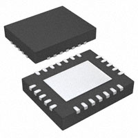
Package:
– 24-QFN (4 mm × 5 mm)
– 24-DSBGA (2.49 mm × 3.49 mm)
Operation Temperature Range: –40°C to 85°C
APPLICATIONS
•
•
•
Portable Audio Player, Cellular Phone
Video Camcorder, Movie Digital Still Camera
PMP/DMB, Voice Recorder
DESCRIPTION
The PCM1870 is a low-power stereo ADC designed
for portable digital audio applications, with line-input
amplifier,
boost
amplifier,
microphone
bias,
programmable gain control, sound effects, and auto
level control (ALC). It is available in 24-QFN (4-mm ×
5-mm) and 24-DSBGA (2.49-mm × 3.49-mm)
packages to save footprint. The PCM1870 accepts
right-justified, left-justified, I2S, and DSP formats,
providing easy interfacing to audio DSP and encoder
chips. Sampling rates up to 50 kHz are supported.
The user-programmable functions are accessible
through a 2- or 3-wire serial control port.
1
Please be aware that an important notice concerning availability, standard warranty, and use in critical applications of
Texas Instruments semiconductor products and disclaimers thereto appears at the end of this data sheet.
PRODUCTION DATA information is current as of publication date.
Products conform to specifications per the terms of the Texas
Instruments standard warranty. Production processing does not
necessarily include testing of all parameters.
Copyright © 2007, Texas Instruments Incorporated
�PCM1870
www.ti.com
SLAS544A – MAY 2007 – REVISED SEPTEMBER 2007
This integrated circuit can be damaged by ESD. Texas Instruments recommends that all integrated circuits be handled with
appropriate precautions. Failure to observe proper handling and installation procedures can cause damage.
ESD damage can range from subtle performance degradation to complete device failure. Precision integrated circuits may be more
susceptible to damage because very small parametric changes could cause the device not to meet its published specifications.
ABSOLUTE MAXIMUM RATINGS
over operating free-air temperature range (unless otherwise noted) (1)
VDD, VIO, VCC
Supply voltage
Ground voltage differences: DGND, AGND, PGND
Input voltage
Input current (any pins except supplies)
UNIT
–0.3 to 4
V
±0.1
V
–0.3 to 4
V
±10
mA
Ambient temperature under bias
–40 to 110
°C
Storage temperature
–55 to 150
°C
Junction temperature
150
°C
260 / 5
°C / s
260
°C
Lead temperature (soldering)
Package temperature (reflow, peak)
(1)
PCM1870
Stresses beyond those listed under absolute maximum ratings may cause permanent damage to the device. These are stress ratings
only, and functional operation of the device at these or any other conditions beyond those indicted under recommended operating
conditions is not impled. Exposure to absolute-maximum-rated conditions for extended periods may affect device reliabiltiy.
RECOMMENDED OPERATING CONDITIONS
MIN
NOM
MAX
UNIT
VCC
Analog supply voltage
2.4
3.3
3.6
V
VDD, VIO
Digital supply voltage
1.71
3.3
3.6
V
Digital input logic family
Digital input clock frequency
CMOS
SCKI system clock
LRCK sampling clock
3.072
18.432
MHz
8
48
kHz
10
pF
85
°C
Digital output load capacitance
TA
2
Operating free-air temperature
–40
Submit Documentation Feedback
Copyright © 2007, Texas Instruments Incorporated
Product Folder Link(s): PCM1870
�PCM1870
www.ti.com
SLAS544A – MAY 2007 – REVISED SEPTEMBER 2007
ELECTRICAL CHARACTERISTICS
All specifications at TA = 25°C, VDD = VIO = VCC = VPA = 3.3 V, fS = 48 kHz, system clock = 256 fS, and 16-bit data, unless
otherwise noted
PARAMETER
TEST CONDITIONS
PCM1870RHF, PCM1870YZF
MIN
TYP
MAX
UNIT
AUDIO DATA
Data Format
Resolution
16
Audio data bit length
16
Audio data format
fS
Bits
MSB-first, 2s-complement
Sampling frequency
System clock
Bits
I2S, left-, right-justified, DSP
Audio data interface format
5
50
VDD < 2 V
27
VDD > 2 V
40
kHz
MHz
DIGITAL INPUT/OUTPUT
Logic family
VIH
VIL
IIH
IIL
VOH
VOL
CMOS compatible
0.7 VIO
Input logic level
Input logic current
Output logic level
0.3 VIO
VIN = 3.3 V
10
VIN = 0 V
IOH = –2 mA
–10
0.75 VIO
IOL = 2 mA
0.25 VIO
VDC
μA
VDC
LINE INPUT TO DIGITAL OUTPUT THROUGH ADC (AIN1L/R, AIN2L/R AND PGINL/R—ALC = OFF, PG1 = PG2 = PG3 = PG4 = 0 dB
Dynamic Performance
SNR
Full-scale input voltage
0 dB
Dynamic range
EIAJ, A-weighted
Signal-to-noise ratio
EIAJ, A-weighted
83
Channel separation
THD+N
Total harmonic distortion + noise
2.828
Vp-p
1
Vrms
90
dB
90
dB
87
–1 dB
0.009%
dB
0.017%
Analog Input
Center voltage
0.5 VCC
AIN1L, AIN1R, AIN2L, and AIN2R
Input impedance
10
20
PGINL and PGINR, PG3 = PG4 = –12 dB
70
142
PGINL and PGINR, PG3 = PG4 = 30 dB
4.7
9.5
V
kΩ
ANALOG OUTPUTS (AOL AND AOR)
Center voltage
0.5 VCC
Load resistance
V
10
kΩ
Load capacitance
20
pF
MICROPHONE BIAS—ALC = OFF, PG1 = PG2 = PG3 = PG4 = 0 dB
Bias voltage
0.75 VCC
Bias source current
Output noise
mA
6.5
μV
Submit Documentation Feedback
Copyright © 2007, Texas Instruments Incorporated
Product Folder Link(s): PCM1870
V
2
3
�PCM1870
www.ti.com
SLAS544A – MAY 2007 – REVISED SEPTEMBER 2007
ELECTRICAL CHARACTERISTICS (continued)
All specifications at TA = 25°C, VDD = VIO = VCC = VPA = 3.3 V, fS = 48 kHz, system clock = 256 fS, and 16-bit data, unless
otherwise noted
PARAMETER
TEST CONDITIONS
PCM1870RHF, PCM1870YZF
MIN
TYP
MAX
UNIT
FILTER CHARACTERISTICS
Decimation Filter for ADC
Pass band
0.408 fS
Stop band
0.591 fS
Pass-band ripple
Stop-band attenuation
±0.02
f < 3.268 fS
–60
Group delay
dB
dB
17/fS
s
High-Pass Filter for ADC
–3 dB
Frequency response (fc = 4 Hz)
3.74
–0.5 dB
10.66
–0.1 dB
Frequency response (fc = 120 Hz)
Frequency response (fc = 240 Hz)
Hz
24.20
–3 dB
118.77
–0.5 dB
321.75
–0.1 dB
605.52
–3 dB
235.68
–0.5 dB
609.95
–0.1 dB
2601.2
Hz
Hz
POWER SUPPLY AND SUPPLY CURRENT
VIO
VDD
Voltage range
VCC
Supply current
Power dissipation
VIO
1.71
3.3
3.6
VDD
1.71
3.3
3.6
VCC
2.4
VDC
3.3
3.6
BPZ input, all active, no load
8
12
mA
All inputs are held static.
1
10
μA
26.4
39.6
mW
3.3
33
μW
85
°C
BPZ input
All inputs are held static.
TEMPERATURE CONDITION
Operation temperature
θJA
4
–40
Thermal resistance
35
Submit Documentation Feedback
°C/W
Copyright © 2007, Texas Instruments Incorporated
Product Folder Link(s): PCM1870
�PCM1870
www.ti.com
SLAS544A – MAY 2007 – REVISED SEPTEMBER 2007
PIN ASSIGNMENTS
24 23 22
YZF Package
(Top View)
AIN1R
AIN1L
MICB
VCC
AGND
RHF Package
(Top View)
A
21 20
AIN1R
AIN1L
MICB
VCOM
PGINR
PGINL
VCC
AGND
AOR
AOL
AIN2R
AIN2L
B
VCOM
1
19
PGINL
AIN2R
2
18
AOL
AIN2L
3
17
PGINR
MODE
4
16
AOR
MS/ADR
5
15
TEST
MD/SDA
6
14
LRCK
MC/SCL
7
13
BCK
C
11 12
TEST
MODE MS/ADR MD/SDA
LRCK
DGND
VIO
MC/SCL
BCK
SCKI
VDD
DOUT
1
2
3
4
E
F
SCKI
DGND
10
VDD
9
VIO
DOUT
8
D
P0057-01
Table 1. TERMINAL FUNCTIONS
TERMINAL
NAME
NO.
I/O
DESCRIPTION
RHF
YZF
AGND
24
B4
–
Ground for analog
AIN1L
21
A2
I
Analog input 1 for L-channel
AIN1R
20
A1
I
Analog input 1 for R-channel
AIN2L
3
C4
I
Analog input 2 for L-channel
AIN2R
2
C3
I
Analog input 2 for R-channel
AOL
18
C2
O
Microphone amplifier output for L-channel
AOR
16
C1
O
Microphone amplifier output for R-channel
BCK
13
F1
I/O
Serial bit clock
DGND
11
E2
–
Ground for digital
DOUT
8
F4
O
Serial audio data output
LRCK
14
E1
I/O
Left- and right-channel clock
MC/SCL
7
E4
I
Mode control clock for 3-wire / 2-wire interface
MD/SDA
6
D4
I/O
Mode control data for 3-wire / 2-wire interface
MICB
22
A3
O
Microphone bias source output
MODE
4
D2
I
2- or 3-wire interface selection (LOW: SPI, HIGH: I2C)
MS/ADR
5
D3
I
Mode control select for 3-wire / 2-wire interface
PGINL
19
B2
I
Analog input to gain amplifier for L-channel
PGINR
17
B1
I
Analog input to gain amplifier for R-channel
SCKI
12
F2
I
System clock
TEST
15
D1
I
Test Pin. Should be connected to ground.
VCC
23
B3
–
Power supply for analog
VCOM
1
A4
–
Common voltage for analog
VDD
10
F3
–
Power supply for digital core
VIO
9
E3
–
Power supply for digital I/O
Submit Documentation Feedback
Copyright © 2007, Texas Instruments Incorporated
Product Folder Link(s): PCM1870
5
�PCM1870
www.ti.com
SLAS544A – MAY 2007 – REVISED SEPTEMBER 2007
FUNCTIONAL BLOCK DIAGRAM
MD/SDA MC/SCL MS/ADR
MODE
AOL
PGINL TEST
SCKI
DOUT BCK
Clock
Manager
2
Serial Interface (SPI/I C)
LRCK
Audio Interface
Mute
PG1
AIN1L
ATR
MUX3
MUX1
AIN2L
0/+12/+20 dB
ADL
PG3
D2S
DS
ADC
+30 to –12 dB
Digital
Filter
ADR
PG4
+30 to –12 dB
AIN2R
PG2
VCOM
Module That Can Be Powered Up/Down
0/+12/+20 dB
MCB
MICB
Digital
Filter
MUX4
MUX2
AIN1R
DS
ADC
Mic Bias
VCOM
Power On
Reset
COM
AOR
PGINR
VIO
VDD
Power Up/Down
Manager
DGND
VCC
AGND
B0231-01
6
Submit Documentation Feedback
Copyright © 2007, Texas Instruments Incorporated
Product Folder Link(s): PCM1870
�PCM1870
www.ti.com
SLAS544A – MAY 2007 – REVISED SEPTEMBER 2007
TYPICAL PERFORMANCE CURVES
All specifications at TA = 25°C, VDD = VIO = VCC = VPA = 3.3 V, fS = 8 kHz to 48 kHz, system clock = 256 fS and 16-bit data,
unless otherwise noted.
DECIMATION FILTER, STOP-BAND
DECIMATION FILTER, PASS-BAND
0
0.2
–20
Amplitude – dB
Amplitude – dB
0.1
–40
–60
–80
0
–0.1
–100
–120
–0.2
0
1
2
Frequency [´ fS ]
3
4
0
0.1
0.2
0.3
Frequency [´ fS ]
0.4
G001
G002
Figure 1.
Figure 2.
HIGH-PASS FILTER PASS-BAND CHARACTERISTICS
(fC = 4 Hz at 48 kHz)
5
HIGH-PASS FILTER PASS-BAND CHARACTERISTICS
(fC = 120 Hz at 48 kHz)
5
0
0
Amplitude – dB
Amplitude – dB
0.5
–5
–10
–15
–5
–10
–15
–20
–20
0
0.0005
0.001
0.0015
Frequency [´ fS ]
0.002
0
0.005
0.01
Frequency [´ fS ]
0.015
G003
Figure 3.
0.02
G012
Figure 4.
Submit Documentation Feedback
Copyright © 2007, Texas Instruments Incorporated
Product Folder Link(s): PCM1870
7
�PCM1870
www.ti.com
SLAS544A – MAY 2007 – REVISED SEPTEMBER 2007
TYPICAL PERFORMANCE CURVES (continued)
All specifications at TA = 25°C, VDD = VIO = VCC = VPA = 3.3 V, fS = 8 kHz to 48 kHz, system clock = 256 fS and 16-bit data,
unless otherwise noted.
HIGH-PASS FILTER PASS-BAND CHARACTERISTICS
(fC = 240 Hz at 48 kHz)
5
Amplitude – dB
0
–5
–10
–15
–20
0
0.01
0.02
Frequency [´ fS ]
0.03
0.04
G004
Figure 5.
8
Submit Documentation Feedback
Copyright © 2007, Texas Instruments Incorporated
Product Folder Link(s): PCM1870
�PCM1870
www.ti.com
SLAS544A – MAY 2007 – REVISED SEPTEMBER 2007
TYPICAL PERFORMANCE CURVES (continued)
All specifications at TA = 25°C, VDD = VIO = VCC = VPA = 3.3 V, fS = 44.1 kHz, system clock = 256 fS and 16-bit data, unless
otherwise noted.
3 BAND TONE CONTROL (BASS)
15
10
10
5
5
Amplitude – dB
Amplitude – dB
3 BAND TONE CONTROL (BASS, MID, TREBLE)
15
0
–5
–10
0
–5
–10
–15
0.01
–15
0.1
1
10
100
Frequency – Hz
1k
10k
100k
0
400
600
Frequency – Hz
200
800
G005
G006
Figure 6.
Figure 7.
3 BAND TONE CONTROL (MID)
3 BAND TONE CONTROL (TREBLE)
15
15
10
10
5
5
Amplitude – dB
Amplitude – dB
1k
0
–5
–10
0
–5
–10
–15
–15
0
1k
2k
3k
Frequency – Hz
4k
5k
2k
4k
6k
8k
10k
Frequency – Hz
12k
G007
Figure 8.
14k
G008
Figure 9.
Submit Documentation Feedback
Copyright © 2007, Texas Instruments Incorporated
Product Folder Link(s): PCM1870
9
�PCM1870
www.ti.com
SLAS544A – MAY 2007 – REVISED SEPTEMBER 2007
TYPICAL PERFORMANCE CURVES (continued)
All specifications at TA = 25°C, VDD = VIO = VCC = VPA = 3.3 V, fS = 48 kHz, system clock = 256 fS and 16-bit data, unless
otherwise noted.
ADC SNR AT HIGH GAIN (PG1/PG2 = 0 dB)
ADC SNR AT HIGH GAIN (PG1/PG2 = 20 dB)
100
90
fIN = 1 kHz
85
90
80
Single Input
75
Single Input
SNR – dB
SNR – dB
85
Differential Input
70
70
65
60
Differential Input
60
55
50
50
45
fIN = 1 kHz
40
40
0
5
10
15
20
PG3/PG4 Gain – dB
25
30
0
10
15
20
PG3/PG4 Gain – dB
5
G009
25
30
G010
Figure 10.
Figure 11.
THD+N/SNR vs POWER SUPPLY
(ADC TO DIGITAL OUTPUT)
0.012
92
fIN = 1 kHz
0.011
91
0.010
90
0.009
89
SNR – dB
THD+N – %
THD+N
SNR
0.008
88
0.007
87
2
2.5
3
Power Supply – V
3.5
4
G011
Figure 12.
10
Submit Documentation Feedback
Copyright © 2007, Texas Instruments Incorporated
Product Folder Link(s): PCM1870
�PCM1870
www.ti.com
SLAS544A – MAY 2007 – REVISED SEPTEMBER 2007
PCM1870 DESCRIPTION
Analog Input
The AIN1L, AIN1R, AIN2L and AIN2R pins can be used as microphone or line inputs with selectable 0- or 20-dB
boost and 1-Vrms input. All analog inputs have high input impedance (20 kΩ), which is not changed by gain
settings. One pair of inputs is selected by register 87 (AIL[1:0], AIR[1:0]). AIN1L and AIN1R can also be used as
a monaural differential input.
Gain Setting for Analog Input
Analog signals can be adjusted from 30 dB to –12 dB in 1-dB steps after the 0-, 12- or 20-dB boost amplifier.
Gain level can be set for each channel by register 79, 80 (ALV[5:0], ARV[5:0]).
A/D Converter
The ADC includes a multilevel delta-sigma modulator, aliasing filter, decimation filter, high-pass filter and notch
filter and can accept 1 Vrms as full-scale input voltage. The decimation filter has a digital soft mute controlled by
register 81 (RMUL, RMUR), and the high-pass and notch filters can be disabled by register 81 (HPF[1:0]) and
registers 96 through 104 if they are not needed to cancel dc offset or avoid wind noise.
Common Voltage
Unbuffered common voltage. The VCOM pin is normally biased to 0.5 VCC, and it provides common voltage to
internal circuitry. Connecting a 4.7-μF capacitor to this pin is recommended to optimize analog performance.
Microphone Bias
The MICB pin is a microphone bias source for an external microphone, which can provide 2 mA (typ) bias
current.
Auto Level Control (ALC) for Recording
The sound when microphone recording should be adjusted to a suitable level without saturation. The digitally
controlled auto level control (ALC) automatically expands small input signals and compresses large input signals
while recording. Expansion level, compression level, attack time, and recovery time can be selected by register
83. See the bit descriptions of register 83 for detailed settings.
3D Sound
A 3D sound effect is provided by mixing L-channel and R-channel data through a band-pass filter with two
control parameters, mixing ratio and band-pass filter characteristic. The control parameters are set in register 95
(3DP[3:0], 3FLO). The 3D sound effect is applied to the ADC digital output.
3-Band Tone Control
Tone control has bass, midrange, and treble controls that can be adjusted from 12 dB to –12 dB in 1-dB steps by
register 92 to 94 (LGA[4:0], MGA[4:0] and HGA[4:0]). Register 92 (LPAE), which attenuates the digital input
signal automatically, can prevent clipping of the output signal at settings higher than 0 dB for bass control. LPAE
is not effective for midrange and treble control.
High-Pass Filter and Notch Filter
The high-pass filter cuts dc offset in the analog section of the ADC and can be set to 4 Hz, 120 Hz, or 240 Hz at
48-kHz sampling by register 81 (HPF[1:0]).
Notch filters remove noise at particular frequencies, CCD noise, motor noise and other mechanical noise in an
application. The PCM1870 has two notch filters, whose center frequency and frequency bandwidth can be
programmed by registers 96 to 104.
Digital Monaural Mixing
The audio data can be mixed to monaural digital data from stereo digital data in the internal audio interface
section by register 96 (MXEN).
Submit Documentation Feedback
Copyright © 2007, Texas Instruments Incorporated
Product Folder Link(s): PCM1870
11
�PCM1870
www.ti.com
SLAS544A – MAY 2007 – REVISED SEPTEMBER 2007
Zero-Cross Detection
Zero-cross detection minimizes audible zipper noise while changing analog volume and digital attenuation. This
function can be applied to digital input or digital output by register 86 (ZCRS).
Power Up/Down for Each Module
Using register 73 (PBIS), register 82 (PAIR, PAIL, PADS, PMCB, PADR, PADL), and register 90 (PCOM),
unused modules can be powered down to minimize power consumption (13 mW when recording only).
Digital Interface
All digital I/O pins can interface at various power supply voltages. The VIO pin can be connected to a 1.71-V to
3.6-V power supply.
Power Supply
The VCC pin can be connected to 2.4 V to 3.6 V. The VDD pin and VIO pin can be connected to 1.71 to 3.6 V. A
different voltage can be applied to each of these pins (for example, VDD = 1.8 V, VIO = 3.3 V).
12
Submit Documentation Feedback
Copyright © 2007, Texas Instruments Incorporated
Product Folder Link(s): PCM1870
�PCM1870
www.ti.com
SLAS544A – MAY 2007 – REVISED SEPTEMBER 2007
DESCRIPTION OF OPERATION
System Clock Input
The PCM1870 can accept input clocks of various frequencies without a PLL. The clocks are used for clocking of
the digital filters, auto level control, and delta-sigma modulators, and classified into common-audio and
application-specific clocks. Table 2 shows frequencies of the common audio clock and the application-specific
clock. Figure 13 shows timing requirements for system clock inputs. The sampling rate and frequency of the
system clock are determined by settings in register 86 (MSR[2:0]) and register 85 (NPR[5:0]). Note that the
sampling rate of the application-specific clock has a little sampling error. The details are shown in Table 8.
Table 2. Frequency of Common Audio Clock
FREQUENCY
Common audio clock
11.2896, 12.288, 16.9344, 18.432 MHz
Application-specific clock
12, 13, 13.5, 24, 26, 27, 19.2, 19.68, 38.4, 39.36 MHz
tw(SCKH)
0.7 VIO
SCKI
0.3 VIO
tw(SCKL)
T0005-12
PARAMETERS
SYMBOL
MIN
UNIT
System clock pulse duration, high
tw(SCKH)
14
ns
System clock pulse duration, low
tw(SCKL)
14
ns
Figure 13. System Clock Timing
Power-On Reset and System Reset
The power-on-reset circuit outputs reset signal, typically at VDD = 1.2 V, and this circuit does not depend on the
voltage of other power-supplies (VCC, VPA, and VIO). Internal circuits are cleared to default status, then signals
are removed from all analog and digital outputs. The PCM1870 does not require any power supply sequencing.
Register data must be written after turning all power supplies on.
System reset is enabled by setting register 85 (SRST), and all registers are cleared automatically. All circuits are
reset to their default status at once. Note that the PCM1870 has audible pop noise on the analog outputs when
enabling SRST.
Power On/Off Sequence
To reduce audible pop noise, a sequence of register settings is required after turning all power supplies on when
powering up, or before turning the power supplies off when powering down. If some modules are not required for
a particular application or operation, they should be placed in the power-down state after performing the
power-on sequence. The recommended power-on and power-off sequences are shown in Table 3 and Table 4,
respectively.
Submit Documentation Feedback
Copyright © 2007, Texas Instruments Incorporated
Product Folder Link(s): PCM1870
13
�PCM1870
www.ti.com
SLAS544A – MAY 2007 – REVISED SEPTEMBER 2007
Table 3. Recommended Power-On Sequence
(1)
(2)
(3)
STEP
REGISTER
SETTINGS
1
—
2
5102H
ADC audio interface format (left-justified)
3
5A00H
PG1, PG2 gain control (0 dB)
4
4980H
Analog bias power up
5
5601H
Zero-cross detection enable
6
4A01H
VCOM power up
7
523FH
Analog front end (ADL, ADR, D2S, MCB, PG1, 2, 5, 6) power up
8
5711H
Analog input (MUX3, MUX4) select. Analog input (MUX1, MUX2) select
9
4F0CH
Analog input L-ch (PG3) volume (0 dB) (3)
10
500CH
Analog input R-ch (PG4) volume (0 dB) (3)
NOTE
Turn ON all power supplies (1)
(2)
VDD should be turned on first or at the same time with other power supplies. It is recommended to set the register data after turning on
all power supplies and while the system clock is running.
The audio interface format should be set to match the DSP or decoder being used.
Any level is acceptable for volume or attenuation. The level should return to that recorded in the register data when system was last
powered off.
Table 4. Recommended Power-Off Sequence
(1)
(2)
14
STEP
REGISTER
SETTINGS
1
5132H
ADC L-ch/R-ch digital soft mute enable, ADC audio interface format (left-justified) (1)
2
5200H
Analog front end (ADL, ADR, D2S, MCB, PG1, 2, 5, 6) power down
3
4A00H
VCOM power down
4
4900H
Analog bias power down
5
—
NOTE
Turn OFF all power supplies.
(2)
The audio interface format should be set to match the DSP or decoder being used.
Power-supply sequencing is not required. It is recommended to make the required register settings while the system clock is running,
then turn off all power supplies.
Submit Documentation Feedback
Copyright © 2007, Texas Instruments Incorporated
Product Folder Link(s): PCM1870
�PCM1870
www.ti.com
SLAS544A – MAY 2007 – REVISED SEPTEMBER 2007
Power-Supply Current
The current consumption of the PCM1870 depends on the power-up/down status of each circuit module. In order
to save power consumption, disabling each module is recommended when it is not used in an appliction or
operation. Table 5 shows current consumtption in some states.
Table 5. Power Consumption Table
POWER SUPPLY CURRENT [mA]
OPERATION MODE
PD [mW]
VDD
(1.8 V)
VDD
(3.3 V)
VCC
(3.3 V)
VIO
(3.3 V)
TOTAL
(VDD = 1.8 V)
TOTAL
(VDD = 3.3 V)
0.000
0.000
0.001
0.000
0.003
0.003
Line input (AIN2L/AIN2R)
1.78
3.71
4.58
0.10
18.3
27.7
Mic input (AIN1L/AIN1R, 20 dB)
1.79
3.71
5.06
0.10
19.9
29.3
Mic input (AIN1L/AIN1R, 20 dB) with ALC
2.73
5.59
5.06
0.10
21.6
35.5
Mono mic input (AIN1L, 20 dB)
1.33
2.80
3.56
0.10
14.1
21.3
Mono mic input (AIN1L, 20 dB) with ALC
2.21
4.60
3.56
0.10
15.7
27.3
Mono diff mic input (AIN1L/AIN1R, 20 dB)
1.33
2.80
3.88
0.10
15.2
22.4
Mono diff mic input (AIN1L/AIN1R, 20 dB) with ALC
2.21
4.60
3.88
0.10
16.8
28.3
Line input (AIN2L/AIN2R)
0.82
1.66
3.71
0.10
13.7
18.1
Mic input (AIN1L/AIN1R, 20 dB)
0.82
1.66
4.20
0.10
15.3
19.7
Mic input (AIN1L/AIN1R, 20 dB) with ALC
1.26
2.55
4.20
0.10
16.1
22.6
Mono mic input (AIN1L, 20 dB)
0.61
1.23
2.74
0.10
10.1
13.4
Mono mic input (AIN1L, 20 dB) with ALC
1.03
2.10
2.74
0.10
10.9
1.63
Mono diff mic input (AIN1L/AIN1R, 20 dB)
0.61
1.23
3.06
0.10
11.2
14.5
Mono diff mic input (AIN1L/AIN1R, 20 dB) with ALC
1.02
2.08
3.06
0.10
11.9
17.3
Line input (AIN2L/AIN2R)
0.59
1.18
3.51
0.10
12.7
15.8
Mic input (AIN1L/AIN1R, 20 dB)
0.59
1.18
3.99
0.10
14.2
17.4
Mic input (AIN1L/AIN1R, 20 dB) with ALC
0.91
1.85
3.99
0.10
14.8
19.6
Mono mic input (AIN1L, 20 dB)
0.44
0.87
2.55
0.10
9.2
11.6
Mono mic input (AIN1L, 20 dB) with ALC
0.75
1.52
2.55
0.10
9.8
13.8
Mono diff mic input (AIN1L/AIN1R, 20 dB)
0.44
0.87
2.87
0.10
10.3
12.7
Mono diff mic input (AIN1L/AIN1R, 20 dB) with ALC
0.74
1.50
2.87
0.10
10.8
14.8
Line input (AIN2L/AIN2R)
0.29
0.54
3.23
0.10
11.2
12.8
Mic input (AIN1L/AIN1R, 20 dB)
0.29
0.54
3.72
0.10
12.8
14.4
Mic input (AIN1L/AIN1R, 20 dB) with ALC
0.46
0.88
3.72
0.10
13.1
15.5
Mono mic input (AIN1L, 20 dB)
0.22
0.39
2.29
0.10
8.0
9.2
Mono mic input (AIN1L, 20 dB) with ALC
0.37
0.70
2.29
0.10
8.2
10.2
Mono diff mic input (AIN1L/AIN1R, 20 dB)
0.22
0.39
2.61
0.10
9.0
10.2
Mono diff mic input (AIN1L/AIN1R, 20 dB) with ALC)
0.37
0.70
2.61
0.10
9.3
11.3
ALL POWER DOWN
Recording (fS = 48 kHz)
Recording (fS = 22.05 kHz)
Recording (fS = 16 kHz)
Recording (fS = 8 kHz)
Condition: 256 fS, 16 bits, slave mode, zero data input, no load
Submit Documentation Feedback
Copyright © 2007, Texas Instruments Incorporated
Product Folder Link(s): PCM1870
15
�PCM1870
www.ti.com
SLAS544A – MAY 2007 – REVISED SEPTEMBER 2007
Audio Serial Interface
The audio serial interface of the PCM1870 consists of LRCK, BCK and DOUT. Sampling rate (fS), left and right
channel are present on LRCK. DOUT transmits the serial data from the decimation filter for the ADC. BCK is
used to transmit the serial audio data on DOUT at its high-to-low transition. BCK and LRCK should be
synchronized with audio system clock. Ideally, it is recommended that they are derived from it.
The PCM1870 requires LRCK to be synchronized with the system clock. The PCM1870 do not need a specific
phase relationship between LRCK and the system clock.
The PCM1870 has both master mode and slave mode interface formats, which can be selected by register 84
(MSTR). LRCK and BCK are generated from the system clock in master mode.
Audio Data Formats and Timing
The PCM1870 supports I2S, right-justified, left-justified, and DSP formats. The data formats are shown in
Figure 16, and they are selected using resister 70 (RFM[1:0], PFM[1:0]). All formats require binary
2s-complement, MSB-first audio data. The default format is I2S. Figure 14 shows a detailed timing diagram.
50% of VIO
LRCK
tw(BCL)
tw(BCH)
t(LB)
50% of VIO
BCK
t(BL)
t(BCY)
t(CKDO)
t(LRDO)
50% of VIO
DOUT
T0010-12
PARAMETERS
SYMBOL
2
MIN
MAX
UNIT
(1)
BCK pulse cycle time (I S, left- and right-justified formats)
t(BCY)
1/(64fS)
BCK pulse cycle time (DSP format)
t(BCY)
1/(256fS) (1)
BCK high-level time
tw(BCH)
35
ns
BCK low-level time
tw(BCL)
35
ns
BCK rising edge to LRCK edge
t(BL)
10
ns
LRCK edge to BCK rising edge
t(LB)
10
DOUT delay time from BCK falling edge
(1)
16
fS is the sampling frequency.
t(CKDO)
ns
40
ns
Figure 14. Audio Interface Timing (Slave Mode)
Submit Documentation Feedback
Copyright © 2007, Texas Instruments Incorporated
Product Folder Link(s): PCM1870
�PCM1870
www.ti.com
SLAS544A – MAY 2007 – REVISED SEPTEMBER 2007
t(SCY)
50% of VIO
SCKI
t(DL)
50% of VIO
LRCK (Output)
tw(BCL)
tw(BCH)
t(DB)
t(DB)
50% of VIO
BCK (Output)
t(BCY)
DOUT
50% of VIO
t(DS)
t(DH)
T0011-05
PARAMETERS
SYMBOL
MIN
1/(256fS)
MAX
UNIT
(1)
SCKI pulse cycle time
t(SCY)
LRCK edge from SCKI rising edge
t(DL)
5
140
ns
BCK edge from SCKI rising edge
t(DB)
5
140
ns
BCK pulse cycle time
t(BCY)
BCK high-level time
tw(BCH)
146
ns
BCK low-level time
tw(BCL)
146
ns
DOUT setup time
t(DS)
10
ns
DOUT hold time
t(DH)
10
ns
(1)
1/(64fS)
(1)
fS is up to 48 kHz. fS is the sampling frequency
Figure 15. Audio Interface Timing (Master Mode)
Submit Documentation Feedback
Copyright © 2007, Texas Instruments Incorporated
Product Folder Link(s): PCM1870
17
�PCM1870
www.ti.com
SLAS544A – MAY 2007 – REVISED SEPTEMBER 2007
(a) Right-Justified Data Format; L-Channel = HIGH, R-Channel = LOW
1/fS
LRCK
L-Channel
R-Channel
BCK
(1)
(= 32 fS, 48 fS, or 64 fS)
16-Bit Right-Justified
DOUT
15 16
1
2
3
4
5
6
7
8
9
10 11 12 13 14 15 16
MSB
1
LSB
2
3
4
5
6
7
8
9
10 11 12 13 14 15 16
MSB
LSB
2
(b) I S Data Format; L-Channel = LOW, R-Channel = HIGH
1/fS
LRCK
L-Channel
R-Channel
BCK
(1)
(= 32 fS, 48 fS, or 64 fS)
DOUT
1
2
3
4
5
6
7
8
9
10 11 12 13 14 15 16
MSB
1
LSB
2
3
4
5
6
7
8
9
10 11 12 13 14 15 16
MSB
1
2
1
2
1
2
1
2
LSB
(c) Left-Justified Data Format; L-Channel = HIGH, R-Channel = LOW
1/fS
LRCK
L-Channel
R-Channel
BCK
(1)
(= 32 fS, 48 fS, or 64 fS)
DOUT
1
2
3
4
5
6
7
8
9
10 11 12 13 14 15 16
MSB
1
LSB
2
3
4
5
6
7
8
9
10 11 12 13 14 15 16
MSB
LSB
(d) Burst BCK Interface Format in Master Mode; L-Channel = HIGH, R-Channel = LOW
1/fS
LRCK
L-Channel
R-Channel
BCK
(1)
(= 32 fS, 48 fS, or 64 fS)
DOUT
1
2
3
4
5
6
7
8
9
MSB
10 11 12 13 14 15 16
1
LSB
2
3
4
5
6
7
8
9
10 11 12 13 14 15 16
MSB
LSB
(e) DSP Format
1/fS
LRCK
BCK
(= 32 fS, 48 fS, 64 fS, 128 fS or 256 fS)
DOUT
1
2
3
4
5
6
7
8
9
MSB
(1)
10 11 12 13 14 15 16
LSB
1
2
3
4
5
6
7
8
9
10 11 12 13 14 15 16
MSB
LSB
T0009-09
All audio interface formats support BCK = 64 fS in master mode (register 69, MSTR = 1). When set to multisampling
rate, fS of BCK is set to half the rate of the DSM operation frequency.
Figure 16. Audio Data Output Formats
18
Submit Documentation Feedback
Copyright © 2007, Texas Instruments Incorporated
Product Folder Link(s): PCM1870
�PCM1870
www.ti.com
SLAS544A – MAY 2007 – REVISED SEPTEMBER 2007
THREE-WIRE INTERFACE (SPI, MODE (PIN 28) = LOW)
All write operations for the serial control port use 16-bit data words. Figure 17 shows the control data word
format. The most significant bit must be 0. There are seven bits, labeled IDX[6:0], that set the register address
for the write operation. The least-significant eight bits, D[7:0], contain the data to be written to the register
specified by IDX[6:0].
Figure 18 shows the functional timing diagram for writing to the serial control port. To write the data into the
mode register, the data is clocked into an internal shift register on the rising edge of the MC clock. The serial
data should change on the falling edge of the MC clock and should be LOW during write mode. The rising edge
of MS should be aligned with the falling edge of the last MC clock pulse in the 16-bit frame. The MC can run
continuously between transactions while MS is in the LOW state.
LSB
MSB
0
IDX6
IDX5
IDX4
IDX3
IDX2
IDX1
IDX0
D7
D6
D5
Register Index (or Address)
D4
D3
D2
D1
D0
Register Data
R0001-01
Figure 17. Control Data Word Format for MD
(1) Single Write Operation
16 Bits
MS
MC
MD
MSB
LSB
MSB
(2) Continuous Write Operation
8 Bits x N Frames
MS
MC
MD
MSB
LSB MSB
Register Index
8 Bits
LSB MSB
Register (N) Data
LSB
Register (N+1) Data
MSB
LSB
Register (N+2) Data
N Frames
T0012-03
Figure 18. Register Write Operation
Submit Documentation Feedback
Copyright © 2007, Texas Instruments Incorporated
Product Folder Link(s): PCM1870
19
�PCM1870
www.ti.com
SLAS544A – MAY 2007 – REVISED SEPTEMBER 2007
Three-Wire Interface (SPI) Timing Requirements
Figure 19 shows a detailed timing diagram for the serial control interface. These timing parameters are critical for
proper control port operation.
tw(MHH)
MS
50% of VIO
t(MLS)
tw(MCL)
tw(MCH)
t(MLH)
MC
50% of VIO
t(MCY)
LSB
MD
50% of VIO
t(MDS)
t(MDH)
T0013-08
PARAMETERS
SYMBOL
MIN
(1)
MC pulse cycle time
t(MCY)
500
MC low-level time
tw(MCL)
50
MC high-level time
tw(MCH)
50
MS high-level time
tw(MHH)
See
TYP
MAX
UNIT
ns
ns
ns
(1)
ns
MS falling edge to MC rising edge
t(MLS)
50
ns
MS hold time
t(MLH)
20
ns
MD hold time
t(MDH)
15
ns
MD setup time
t(MDS)
20
ns
(1)
3/(128 fS) s (min), where fS is the sampling frequency
A
Figure 19. SPI Interface Timing
20
Submit Documentation Feedback
Copyright © 2007, Texas Instruments Incorporated
Product Folder Link(s): PCM1870
�PCM1870
www.ti.com
SLAS544A – MAY 2007 – REVISED SEPTEMBER 2007
TWO-WIRE INTERFACE [I2C, MODE (PIN 28) = HIGH]
The PCM1870 supports the I2C serial bus and the data transmission protocol for the I2C standard as a slave
device. This protocol is explained in I2C specification 2.0.
In I2C mode, the control terminals are changed as follows.
TERMINAL NAME
PROPERTY
DESCRIPTION
MS/ADR
Input
I2C address
MD/SDA
Input/output
I2C data
MC/SCL
Input
I2C clock
Slave Address
MSB
LSB
1
0
0
0
1
1
ADR
R/W
The PCM1870 has its 7-bit slave address. The first six bits (MSBs) of the slave address are factory preset to
1000 11. The next bit of the address byte is the device select bit, which can be user-defined by ADR terminal. A
maximum of two PCM1870s can be connected on the same bus at one time. Each PCM1870 responds when it
receives its own slave address.
Packet Protocol
A master device must control packet protocol, which is start condition, slave address with read/write bit, data if
write or acknowledgement if read, and stop condition. The PCM1870 supports only slave-receiver and
slave-transmitter.
SDA
SCL
St
1−7
8
9
1−8
9
1−8
9
Sp
Slave Address
R/W
ACK
DATA
ACK
DATA
ACK
R/W: Read Operation if 1; Otherwise, Write Operation
ACK: Acknowledgement of a Byte if 0
DATA: 8 Bits (Byte)
Start
Condition
Stop
Condition
Write Operation
Transmitter
M
M
M
S
M
S
M
S
M
Data Type
St
Slave Address
R/W
ACK
DATA
ACK
DATA
ACK
Sp
Read Operation
Transmitter
M
M
M
S
S
M
S
M
M
Data Type
St
Slave Address
R/W
ACK
DATA
ACK
DATA
NACK
Sp
M: Master Device
St: Start Condition
S: Slave Device
Sp: Stop Condition
T0049-03
2
Figure 20. Basic I C Framework
Submit Documentation Feedback
Copyright © 2007, Texas Instruments Incorporated
Product Folder Link(s): PCM1870
21
�PCM1870
www.ti.com
SLAS544A – MAY 2007 – REVISED SEPTEMBER 2007
Write Operation
A master can write any PCM1870 registers using single access. The master sends a PCM1870 slave address
with a write bit, a register address, and the data. When undefined registers are accessed, the PCM1870 does not
send an acknowledgement. The Figure 21 shows a diagram of the write operation.
Transmitter
M
M
M
S
M
S
M
S
M
Data Type
St
Slave Address
W
ACK
Reg Address
ACK
Write Data
ACK
Sp
M: Master Device S: Slave Device
St: Start Condition W: Write ACK: Acknowledge Sp: Stop Condition
R0002-01
Figure 21. Framework for Write Operation
Read Operation
A master can read the PCM1870 register. The value of the register address is stored in an indirect index register
in advance. The master sends a PCM1870 slave address with a read bit after storing the register address. Then
the PCM1870 transfers the data which the index register points to. Figure 22 shows a diagram of the read
operation.
Transmitter
M
M
M
S
M
S
M
M
M
S
Data Type
St
Slave Address
W
ACK
Reg Address
ACK
Sr
Slave Address
R
ACK
S
M
M
Read Data NACK Sp
M: Master Device S: Slave Device St: Start Condition
Sr: Repeated Start Condition ACK: Acknowledge Sp: Stop Condition NACK: Not Acknowledge
W: Write R: Read
R0002-02
NOTE: The slave address after the repeated start condition must be the same as the previous slave address.
Figure 22. Read Operation
22
Submit Documentation Feedback
Copyright © 2007, Texas Instruments Incorporated
Product Folder Link(s): PCM1870
�PCM1870
www.ti.com
SLAS544A – MAY 2007 – REVISED SEPTEMBER 2007
Timing Diagram
Start
Stop
t(D-HD)
t(BUF)
t(SDA-F)
t(D-SU)
t(SDA-R)
t(P-SU)
SDA
t(SCL-R)
t(RS-HD)
t(SP)
t(LOW)
SCL
t(S-HD)
t(HI)
t(RS-SU)
t(SCL-F)
T0050-03
TIMING CHARACTERISTICS
SYMBOL
PARAMETER
CONDITIONS
MIN
MAX
UNIT
100
kHz
fSCL
SCL clock frequency
Standard
t(BUF)
Bus free time between a STOP and START condition
Standard
4.7
μs
t(LOW)
Low period of the SCL clock
Standard
4.7
μs
t(HI)
High period of the SCL clock
Standard
4
μs
t(RS-SU)
Setup time for START condition
Standard
4.7
μs
t(S-HD)
Hold time for START condition
Standard
4
μs
t(D-SU)
Data setup time
Standard
250
t(D-HD)
Data hold time
Standard
0
900
ns
t(SCL-R)
Rise time of SCL signal
Standard
20 + 0.1 CB
1000
ns
t(SCL-F)
Fall time of SCL signal
Standard
20 + 0.1 CB
1000
ns
t(SDA-R)
Rise time of SDA signal
Standard
20 + 0.1 CB
1000
ns
t(SDA-F)
Fall time of SDA signal
Standard
20 + 0.1 CB
1000
ns
t(P-SU)
Setup time for STOP condition
Standard
4
CB
Capacitive load for SDA and SCL line
400
pF
t(SP)
Pulse duration of spike suppressed
25
ns
ns
μs
Figure 23. I2C Interface Timing
Submit Documentation Feedback
Copyright © 2007, Texas Instruments Incorporated
Product Folder Link(s): PCM1870
23
�PCM1870
www.ti.com
SLAS544A – MAY 2007 – REVISED SEPTEMBER 2007
USER-PROGRAMMABLE MODE CONTROLS
Register Map
The mode control register map is shown in Table 6. Each register includes an index (or address) indicated by the
IDX[6:0] bits.
Table 6. Mode Control Register Map
REGISTER
IDX [6:0]
(B14–B8)
DESCRIPTION
B7
B6
B5
B4
B3
B2
B1
B0
Register 73
49h
Analog bias power up/down
PBIS
RSV
RSV
RSV
RSV
RSV
RSV
RSV
Register 74
4Ah
VCOM power up/down
RSV
RSV
RSV
RSV
RSV
RSV
RSV
PCOM
Register 79
4Fh
Volume for ADC input (L-ch)
RSV
RSV
ALV5
ALV4
ALV3
ALV2
ALV1
ALV0
Register 80
50h
Volume for ADC input (R-ch)
RSV
RSV
ARV5
ARV4
ARV3
ARV2
ARV1
ARV0
Register 81
51h
ADC high pass-filter, soft mute, audio interface
HPF1
HPF0
RMUL
RMUR
RSV
DSMC
RFM1
RFM0
Register 82
52h
ADC, MCB, PG1, 2, 5, 6, D2S power up/down
Register 83
53h
Auto level control for recording
Register 84
54h
Master mode
Register 85
55h
Register 86
Register 87
RSV
RSV
PAIR
PAIL
PADS
PMCB
PADR
PADL
RALC
RSV
RRTC
RATC
RCP1
RCP0
RLV1
RLV0
RSV
RSV
RSV
RSV
RSV
MSTR
RSV
BIT0
System reset, sampling rate control
SRST
RSV
NPR5
NPR4
NPR3
NPR2
NPR1
NPR0
56h
BCK config, master mode, zero cross
MBST
MSR2
MSR1
MSR0
RSV
RSV
RSV
ZCRS
57h
Analog input select (MUX1, 2, 3, 4)
AD2S
RSV
AIR1
AIR0
RSV
RSV
AIL1
AIL0
Register 90
5Ah
VCOM power up/down, ramp up/down time, boost
RSV
RSV
RSV
RSV
RSV
RSV
G20R
G20L
Register 92
5Ch
Bass boost gain level (200 Hz)
LPAE
RSV
RSV
LGA4
LGA3
LGA2
LGA1
LGA0
Register 93
5Dh
Middle boost gain level (1 kHz)
RSV
RSV
RSV
MGA4
MGA3
MGA2
MGA1
MGA0
Register 94
5Eh
Treble boost gain level (5 kHz)
RSV
RSV
RSV
HGA4
HGA3
HGA2
HGA1
HGA0
Register 95
5Fh
Sound effect source select, 3D sound
RSV
3DEN
RSV
3FL0
3DP3
3DP2
3DP1
3DP0
Register 96
60h
2-stage notch filter, digital monaural mixing
NEN2
NEN1
NUP2
NUP1
RSV
RSV
RSV
MXEN
Register 97
61h
1st-stage notch filter lower coefficient (a1)
F107
F106
F105
F104
F103
F102
F101
F100
Register 98
62h
1st-stage notch filter upper coefficient (a1)
F115
F114
F113
F112
F111
F110
F109
F108
Register 99
63h
1st-stage notch filter lower coefficient (a2)
F207
F206
F205
F204
F203
F202
F201
F200
Register 100
64h
1st-stage notch filter upper coefficient (a2)
F215
F214
F213
F212
F211
F210
F209
F208
Register 101
65h
2nd-stage notch filter lower coefficient (a1)
S107
S106
S105
S104
S103
S102
S101
S100
Register 102
66h
2nd-stage notch filter upper coefficient (a1)
S115
S114
S113
S112
S111
S110
S109
S108
Register 103
67h
2nd-stage notch filter lower coefficient (a2)
S207
S206
S205
S204
S203
S202
S201
S200
Register 104
68h
2nd-stage notch filter upper coefficient (a2)
S215
S214
S213
S212
S211
S210
S209
S208
Register 124
7Ch
Mic boost
RSV
RSV
RSV
RSV
RSV
RSV
G12R
G12L
ADC: A/D converter
MCB: Microphone bias
PGx: Analog input buffer
24
D2S: Differential to single-ended amplifier
Submit Documentation Feedback
Copyright © 2007, Texas Instruments Incorporated
Product Folder Link(s): PCM1870
�PCM1870
www.ti.com
SLAS544A – MAY 2007 – REVISED SEPTEMBER 2007
Register 73
B15
Register 73
0
B14
B13
B12
B11
B10
B9
IDX6 IDX5 IDX4 IDX3 IDX2 IDX1
B8
B7
B6
B5
B4
B3
B2
B1
B0
IDX0
PBIS
RSV
RSV
RSV
RSV
RSV
RSV
RSV
IDX[6:0]: 100 1001b (49h) Register 73
PBIS: Power Up/Down Control for Bias
Default value: 0
This bit is used to control power up/down for the analog bias circuit.
PBIS = 0
Power down (default)
PBIS = 1
Power up
Register 74
B15
Register 74
0
B14
B13
B12
B11
B10
B9
IDX6 IDX5 IDX4 IDX3 IDX2 IDX1
B8
B7
B6
B5
B4
B3
B2
B1
B0
IDX0
RSV
RSV
RSV
RSV
RSV
RSV
RSV
PCOM
IDX[6:0]: 100 1010b (4Ah) Register 74
PCOM: Power Up/Down Control for VCOM
Default value: 0
This bit is used to control power up/down for VCOM.
PCOM = 0
Power down (default)
PCOM = 1
Power up
Submit Documentation Feedback
Copyright © 2007, Texas Instruments Incorporated
Product Folder Link(s): PCM1870
25
�PCM1870
www.ti.com
SLAS544A – MAY 2007 – REVISED SEPTEMBER 2007
Register 79 and 80
B15
B14
B13
B12
B11
B10
B9
B8
B7
B6
B5
B4
B3
B2
B1
B0
Register 79
0
IDX6 IDX5 IDX4 IDX3 IDX2 IDX1
IDX0
RSV
RSV
ALV5
ALV4
ALV3
ALV2
ALV1
ALV0
Register 80
0
IDX6 IDX5 IDX4 IDX3 IDX2 IDX1
IDX0
RSV
RSV
ARV5
ARV4
ARV3
AR2
ARV1
ARV0
IDX[6:0]: 100 1111b (4Fh) Register 79
IDX[6:0]: 101 0000b (50h) Register 80
ALV[5:0]: Gain Control for PG3 (ADC Analog Input R-Channel)
ARV[5:0]: Gain Control for PG4 (ADC Analog Input L-Channel)
Default value: 00
PG3 and PG4 can be independently controlled for ADC input from 30 dB to –12 dB in 1-dB steps. ADC output
may have zipper noise when changing levels. In the PCM1870, the noise can be reduced when making the
change by using zero-cross detection (Register 85, ZCRS).
Table 7. Gain Level Setting
ALV[5:0], ARV[5:0]
26
BINARY
HEX
10 1010
2A
10 1001
29
10 1000
10 0111
GAIN LEVEL SETTING
ALV[5:0], ARV[5:0]
GAIN LEVEL SETTING
BINARY
HEX
30 dB
01 0100
14
8 dB
29 dB
01 0011
13
7 dB
28
28 dB
01 0010
12
6 dB
27
27 dB
01 0001
11
5 dB
10 0110
26
26 dB
01 0000
10
4 dB
10 0101
25
25 dB
00 1111
0F
3 dB
10 0100
24
24 dB
00 1110
0E
2 dB
10 0011
23
23 dB
00 1101
0D
1 dB
10 0010
22
22 dB
00 1100
0C
0 dB
10 0001
21
21 dB
00 1011
0B
–1 dB
10 0000
20
20 dB
00 1010
0A
–2 dB
01 1111
1F
19 dB
00 1001
09
–3 dB
01 1110
1E
18 dB
00 1000
08
–4 dB
01 1101
1D
17 dB
00 0111
07
–5 dB
01 1100
1C
16 dB
00 0110
06
–6 dB
01 1011
1B
15 dB
00 0101
05
–7 dB
01 1010
1A
14 dB
00 0100
04
–8 dB
01 1001
19
13 dB
00 0011
03
–9 dB
01 1000
18
12 dB
00 0010
02
–10 dB
01 0111
17
11 dB
00 0001
01
–11 dB
01 0110
16
10 dB
00 0000
00
–12 dB (default)
01 0101
15
9 dB
Submit Documentation Feedback
Copyright © 2007, Texas Instruments Incorporated
Product Folder Link(s): PCM1870
�PCM1870
www.ti.com
SLAS544A – MAY 2007 – REVISED SEPTEMBER 2007
Register 81
B15
Register 81
0
B14
B13
B12
B11
B10
B9
IDX6 IDX5 IDX4 IDX3 IDX2 IDX1
B8
B7
B6
IDX0
HPF1
HPF0
B5
B4
RMUL RMUR
B3
RSV
B2
B1
DSMC RFM1
B0
RFM0
IDX[6:0]: 101 0001b (51h) Register 81
HPF[1:0]: High-Pass Filter Selection
Default value: 00
The PCM1870 has a digital high-pass filter to remove dc voltage at the input of the ADC. The cutoff frequency of
the high-pass filter can be selected.
HPF[1:0]
High Pass Filter Selection
00
fC = 4 Hz at 48 kHz (default)
01
fC = 240 Hz at 48 kHz
10
fC = 120 Hz at 48 kHz
11
High-pass filter disabled
RMUL: Digital Soft Mute Control for ADC L-Channel
RMUR: Digital Soft Mute Control for ADC R-Channel
Default value: 1
The digital output of the ADC can be independently muted or unmuted. The transition from the current volume
level to mute, or the return to the previous volume setting from mute, occurs at the rate of one 1-dB step for each
8/fS time period. When RMUL and RMUR = 0, the digital data is increased from mute to the previous attenuation
level, and when RMUL and RMUR = 1, the digital data is decreased from the current attenuation level to mute. In
the PCM1870, audible zipper noise can be reduced by using zero-cross detection (register 85, ZCRS).
RMUL, RMUR = 0
Mute disabled
RMUL, RMUR = 1
Mute enabled (default)
DSMC: Waiting Time Turn ADC Mute Off at Power Up
Default value: 0
ADC digital output has waiting time at power up when DSMC = 0. It is recommended to set DSMC = 0.
DSMC = 0
10 ms at 48 kHz (default)
DSMC = 1
No wait
RFM[1:0]: Audio Interface Selection for ADC (Digital Output)
Default value: 00
The audio interface format for ADC digital output has I2S, right-justified, left-justified, and DSP formats.
RFM[1:0]
Audio Interface Selection for ADC Digital Output
00
I2S (default)
01
Right-justified
10
Left-justified
11
DSP mode
Submit Documentation Feedback
Copyright © 2007, Texas Instruments Incorporated
Product Folder Link(s): PCM1870
27
�PCM1870
www.ti.com
SLAS544A – MAY 2007 – REVISED SEPTEMBER 2007
Register 82
B15
Register 82
0
B14
B13
B12
B11
B10
B9
IDX6 IDX5 IDX4 IDX3 IDX2 IDX1
B8
B7
B6
B5
B4
B3
IDX0
RSV
RSV
PAIR
PAIL
PADS
B2
B1
PMCB PADR
B0
PADL
IDX[6:0]: 101 0010b (52h) Register 82
PAIR: Power Up/Down for PG2 and PG6 (Gain Amplifier for Analog Input R-Channel)
PAIR: Power Up/Down for PG1 and PG5 (Gain Amplifier for Analog Input L-Channel)
Default value: 0
This bit is used to control power up/down for PG1, -2 and PG5, -6 (gain amplifier for analog input).
PAIR, PAIL = 0
Power down (default)
PAIR, PAIL = 1
Power up
PADS: Power Up/Down for D2S (Differential Amplifier) of AIN1L and AIN1R
Default value: 0
This bit is used to control power up/down for D2S (differential-to-single amplifier).
PADS = 0
Power down (default)
PADS = 1
Power up
PMCB: Power Up/Down Control for Microphone Bias Source
Default value: 0
This bit is used to control power up/down for the microphone bias source.
PMCB = 0
Power down (default)
PMCB = 1
Power up
PADR: Power Up/Down Control for ADR (ADC and Digital Filter R-Channel)
PADL: Power Up/Down Control for ADL (ADC and Digital Filter L-Channel)
Default value: 0
This bit is used to control power up/down for the ADC and decimation filter.
PADR, PADL = 0
Power down (default)
PADR, PADL = 1
Power up
28
Submit Documentation Feedback
Copyright © 2007, Texas Instruments Incorporated
Product Folder Link(s): PCM1870
�PCM1870
www.ti.com
SLAS544A – MAY 2007 – REVISED SEPTEMBER 2007
Register 83
B15
Register 83
B14
0
B13
B12
B11
B10
B9
IDX6 IDX5 IDX4 IDX3 IDX2 IDX1
B8
B7
B6
B5
B4
B3
B2
B1
B0
IDX0
RALC
RSV
RRTC
RATC
RCP1
RCP0
RLV1
RLV0
IDX[6:0]: 1010011b (53h) Register 83
RALC: Automatic Level Control (ALC) Enable for Recording
Default value: 0
Auto level control can be enabled with some parameters for microphone input or lower-level analog source.
RALC = 0
Disabled (default)
RALC = 1
Enabled
RRTC: ALC Recovery Time Control for Recording
Default value: 0
This bit selects the time during which a gain level change completes to compress the signal when the input to the
ADC increases in amplitude.
RRTC = 0
3.4 s (default)
RRTC = 1
13.6 s
RATC: ALC Attack Time Control for Recording
Default value: 0
This bit selects the time during which a gain level change completes to expand the signal when the input to the
ADC decreases in amplitude.
RATC = 0
1 ms (default)
RATC = 1
2 ms
RCP[1:0]: ALC Compression Level Control for Recording
Default value: 00
Auto level control can set the compression level to –2, –6, or –12 dB. Higher-level signals should be compressed
to avoid saturation or degradation of sound quality.
RCP[1:0]
ALC Compression Level Control for Recording
00
–2 dB (default)
01
–6 dB
10
–12 dB
11
Reserved
RLV[1:0]: ALC Expansion Level Control for Recording
Default value: 00
Auto level control can set the expansion level to 0, 6, 14, or 24 dB. Lower-level signals should be expanded to
make a small signal easy to hear. If set to 0 dB, the ALC can be operated only as a limiter.
RLV[1:0]
ALC Expansion Level Control for Recording
00
0 dB (default)
01
6 dB
10
14 dB
11
24 dB
Submit Documentation Feedback
Copyright © 2007, Texas Instruments Incorporated
Product Folder Link(s): PCM1870
29
�PCM1870
www.ti.com
SLAS544A – MAY 2007 – REVISED SEPTEMBER 2007
Register 84–86
B15
B14
B13
B12
B11
B10
B9
B8
B7
B6
B5
B4
B3
B2
B1
B0
Register 84
0
IDX6 IDX5 IDX4 IDX3 IDX2 IDX1
IDX0
RSV
RSV
RSV
RSV
RSV
MSTR
RSV
BIT0
Register 85
0
IDX6 IDX5 IDX4 IDX3 IDX2 IDX1
IDX0
SRST
RSV
NPR5
NPR4
NPR3
NPR2
NPR1
NPR0
Register 86
0
IDX6 IDX5 IDX4 IDX3 IDX2 IDX1
IDX0
MBST
MSR2
MSR1
MSR0
RSV
RSV
RSV
ZCRS
IDX[6:0]: 101 0100b (54h) Register 84
IDX[6:0]: 101 0101b (55h) Register 85
IDX[6:0]: 101 0110b (56h) Register 86
MSTR: Master or Slave Selection for Audio Interface
Default value: 0
This bit is used to select either master or slave mode for the audio interface. In master mode, PCM1870
generates LRCK and BCK from the system clock. In slave mode, it receives LRCK and BCK from another
device.
MSTR = 0
Slave interface (default)
MSTR = 1
Master interface
BIT0: Bit Length Selection for Audio Interface
Default value: 1
This bit is used to select data bit length for the ADC output.
BIT0 = 0
Reserved
BIT0 = 1
16 bits (default)
SRST: System Reset
Default value: 0
This bit is used to enable system reset. All circuits are reset by setting SRST = 1. After completing the reset
sequence, SRST resets to 0 automatically.
SRST = 0
Reset disabled (default)
SRST = 1
Reset enabled
NPR[5:0]: System Clock Rate Selection
Default value: 00 0000
These bits are used to select the system clock rate. See Table 8 for details.
MBST: BCK Output Configuration in Master Mode
Default value: 0
This bit is used to control the BCK output configuration in master mode. VIO (I/O cell power supply) power
consumption can be reduced by adjusting BCK edge to bit number when setting MBST = 1. This is effective in
master mode (register 69 MSTR = 1).
MBST = 0
Normal output (default)
MBST = 1
Burst output
30
Submit Documentation Feedback
Copyright © 2007, Texas Instruments Incorporated
Product Folder Link(s): PCM1870
�PCM1870
www.ti.com
SLAS544A – MAY 2007 – REVISED SEPTEMBER 2007
MSR[2:0]: System Clock Dividing Rate Selection in Master Mode (Register 70)
Default value: 000
These bits are used to set the dividing rate of the input system clock. See Table 8 for details.
Table 8. System Clock Frequency for Common Audio Clock
SYSTEM CLOCK
SCK (MHz)
ADC SAMPLING RATE
ADC fS (kHz)
6.144
8.192
12.288
18.432
5.6448
11.2896
DAC SAMPLING RATE
DAC fS (kHz)
REGISTER SETTING
MSR[2:0]
NPR[5:0]
BIT CLOCK
BCK (fS)
24 (SCK/256)
010
00 0000
64
16 (SCK/384)
011
00 0000
64
12 (SCK/512)
100
00 0000
64
8 (SCK/768)
101
00 0000
64
6 (SCK/1024)
110
00 0000
64
4 (SCK/1536)
111
00 0000
64
32 (SCK/256)
010
00 0000
64
16 (SCK/512)
100
00 0000
64
8 (SCK/1024)
110
00 0000
64
48 (SCK/256)
010
00 0000
64
32 (SCK/384)
011
00 0000
64
24 (SCK/512)
100
00 0000
64
16 (SCK/768)
101
00 0000
64
12 (SCK/1024)
110
00 0000
64
8 (SCK/1536)
111
00 0000
64
48 (SCK/384)
011
00 0000
64
24 (SCK/768)
101
00 0000
64
12 (SCK/1536)
111
00 0000
64
22.05 (SCK/256)
010
00 0000
64
14.7 (SCK/384)
011
00 0000
64
11.025 (SCK/512)
100
00 0000
64
7.35 (SCK/768)
101
00 0000
64
5.5125 (SCK/1024)
110
00 0000
64
3.675 (SCK/1536)
111
00 0000
64
44.1 (SCK/256)
010
00 0000
64
29.4 (SCK/384)
011
00 0000
64
22.05 (SCK/512)
100
00 0000
64
14.7 (SCK/768)
101
00 0000
64
11.025 (SCK/1024)
110
00 0000
64
7.35 (SCK/1536)
111
00 0000
64
NOTE: Other settings are reserved.
Submit Documentation Feedback
Copyright © 2007, Texas Instruments Incorporated
Product Folder Link(s): PCM1870
31
�PCM1870
www.ti.com
SLAS544A – MAY 2007 – REVISED SEPTEMBER 2007
Table 9. System Clock Frequency for Application-Specific Audio Clock
SYSTEM CLOCK
SCK (MHz)
ADC SAMPLING RATE
ADC fS (kHz)
13.5
27
12
24
19.2
32
DAC SAMPLING RATE
DAC fS (kHz)
REGISTER SETTING
MSR[2:0]
NPR[5:0]
BIT CLOCK
BCK (fS)
48.214 (SCK/280)
010
00 0010
70
44.407 (SCK/304)
010
00 0001
76
32.142 (SCK/420)
010
10 0010
70
24.107 (SCK/560)
100
00 0010
70
22.203 (SCK/608)
100
00 0001
76
16.071 (SCK/840)
100
10 0010
70
12.053 (SCK/1120)
110
00 0010
70
8.035 (SCK/1680)
110
10 0010
70
48.214 (SCK/560)
010
01 0010
70
44.407 (SCK/608)
010
01 0001
76
32.142 (SCK/840)
010
11 0010
70
24.107 (SCK/1120)
100
01 0010
70
22.203 (SCK/1216)
100
01 0001
76
16.071 (SCK/1680)
100
11 0010
70
12.053 (SCK/2240)
110
01 0010
70
8.035 (SCK/3360)
110
11 0010
70
48.387 (SCK/248)
010
00 0100
62
44.117 (SCK/272)
010
00 0011
68
32.258 (SCK/372)
010
10 0100
62
24.193 (SCK/496)
100
00 0100
62
22.058 (SCK/544)
100
00 0011
68
16.129 (SCK/744)
100
10 0100
62
12.096 (SCK/992)
110
00 0100
62
8.064 (SCK/1488)
110
10 0100
62
48.387 (SCK/496)
010
01 0100
62
44.117 (SCK/544)
010
01 0011
68
32.258 (SCK/744)
010
11 0100
62
24.193 (SCK/992)
100
01 0100
62
22.058 (SCK/1088)
100
01 0011
68
16.129 (SCK/1488)
100
11 0100
62
12.096 (SCK/1984)
110
01 0100
62
8.064 (SCK/2796)
110
11 0100
62
48.484 (SCK/396)
011
00 0110
66
44.444 (SCK/432)
011
00 0101
72
32.323 (SCK/594)
011
10 0110
66
24.242 (SCK/792)
101
00 0110
66
22.222 (SCK/864)
101
00 0101
72
16.161 (SCK/1188)
101
10 0110
66
12.121 (SCK/1584)
111
00 0110
66
8.080 (SCK/2376)
111
10 0110
66
Submit Documentation Feedback
Copyright © 2007, Texas Instruments Incorporated
Product Folder Link(s): PCM1870
�PCM1870
www.ti.com
SLAS544A – MAY 2007 – REVISED SEPTEMBER 2007
Table 9. System Clock Frequency for Application-Specific Audio Clock (continued)
SYSTEM CLOCK
SCK (MHz)
ADC SAMPLING RATE
ADC fS (kHz)
38.4
13
26
19.68
39.36
DAC SAMPLING RATE
DAC fS (kHz)
REGISTER SETTING
MSR[2:0]
NPR[5:0]
BIT CLOCK
BCK (fS)
48.484 (SCK/792)
011
01 0110
66
44.444 (SCK/864)
011
01 0101
72
32.323 (SCK/1188)
011
11 0110
66
24.242 (SCK/1584)
101
01 0110
66
22.222 (SCK/1728)
101
01 0101
72
16.161 (SCK/2376)
101
11 0110
66
12.121 (SCK/3168)
111
01 0110
66
8.080 (SCK/4752)
111
11 0110
66
47.794 (SCK/272)
010
00 1000
68
43.918 (SCK/296)
010
00 0111
74
31.862 (SCK/408)
010
10 1000
68
23.897 (SCK/544)
100
00 1000
68
21.959 (SCK/592)
100
00 0111
74
15.931 (SCK/816)
100
10 1000
68
11.948 (SCK/1088)
110
00 1000
68
7.965 (SCK/1632)
110
10 1000
68
47.794 (SCK/544)
010
01 1000
68
43.918 (SCK/592)
010
01 0111
74
31.862 (SCK/816)
010
11 1000
68
23.897 (SCK/1088)
100
01 1000
68
21.959 (SCK/1184)
100
01 0111
74
15.931 (SCK/1632)
100
11 1000
68
11.948 (SCK/2176)
110
01 1000
68
7.965 (SCK/3264)
110
11 1000
68
48.235 (SCK/408)
011
00 1010
68
44.324 (SCK/444)
011
00 1001
74
32.156 (SCK/612)
011
10 1010
68
24.117 (SCK/816)
101
00 1010
68
22.162 (SCK/888)
101
00 1001
74
16.078 (SCK/1224)
101
10 1010
68
12.058 (SCK/1632)
111
00 1010
68
8.039 (SCK/2448)
111
10 1010
68
48.235 (SCK/816)
011
01 1010
68
44.324 (SCK/888)
011
01 1001
74
32.156 (SCK/1224)
011
11 1010
68
24.117 (SCK/1632)
101
01 1010
68
22.162 (SCK/1776)
101
01 1001
74
16.078 (SCK/2448)
101
11 1010
68
12.058 (SCK/3264)
111
01 1010
68
8.039 (SCK/4896)
111
11 1010
68
Submit Documentation Feedback
Copyright © 2007, Texas Instruments Incorporated
Product Folder Link(s): PCM1870
33
�PCM1870
www.ti.com
SLAS544A – MAY 2007 – REVISED SEPTEMBER 2007
ZCRS: Zero Cross for Digital Attenuation/Mute and Analog Gain Setting
Default value: 0
This bit is used to enable the zero-cross detector, which reduces zipper noise while the digital soft mute or
analog gain setting is being changed. If no zero-cross data is input for a 512/fS period (10.6 ms at a 48-kHz
sampling rate), then a time-out occurs and the PCM1870 starts changing the attenuation, gain, or volume level.
The zero-cross detector cannot be used with continuous-zero and dc data.
ZCRS = 0
Zero cross disabled (default)
ZCRS = 1
Zero cross enabled
Register 87
B15
Register 87
B14
0
B13
B12
B11
B10
B9
IDX6 IDX5 IDX4 IDX3 IDX2 IDX1
B8
B7
B6
B5
B4
B3
B2
B1
B0
IDX0
AD2S
RSV
AIR1
AIR0
RSV
RSV
AIL1
AIL0
IDX[6:0]: 101 0111b (57h) Register 87
AD2S: Differential Amplifier Selector (MUX3 and MUX4)
Default value: 0
This bit is used to select whether a single-ended amplifier or differential amplifier (D2S) is used as the input for
the ADC. MUX3 and MUX4 use the single-ended input when AD2S = 0. MUX3 and MUX4 use the monaural
differential input when AD2S = 1.
AD2S = 0
Single-ended amplifier (default)
AD2S = 1
Differential amplifier
AIL[1:0]: AIN1L and AIN2L Selector (MUX1)
Default value: 00
MUX1 selects the analog input, AIN1L or AIN2L.
AIL[1:0]
AIN L-channel Select
00
Disconnect (default)
01
AIN1L
10
AIN2L
11
Reserved
AIR[1:0]: AIN1R and AIN2R Selector (MUX2)
Default value: 00
MUX2 selects the analog input, AIN1R or AIN2R.
AIR[1:0]
AIN R-channel Select
00
Disconnect (default)
01
AIN1R
10
AIN2R
11
Reserved
34
Submit Documentation Feedback
Copyright © 2007, Texas Instruments Incorporated
Product Folder Link(s): PCM1870
�PCM1870
www.ti.com
SLAS544A – MAY 2007 – REVISED SEPTEMBER 2007
Register 90
B15
Register 90
0
B14
B13
B12
B11
B10
B9
IDX6 IDX5 IDX4 IDX3 IDX2 IDX1
B8
B7
B6
B5
B4
B3
B2
B1
B0
IDX0
RSV
RSV
RSV
RSV
RSV
RSV
G20R
G20L
IDX[6:0]: 101 1010b (5Ah) Register 90
G20R: 20-dB Boost for PG2 (Gain Amplifier for AIN1R and AIN2R)
Default value: 0
This bit is used to boost the microphone signal when the analog input is small.
G12R
(REGISTER 124)
G20R
(REGISTER 90)
PG2 GAIN
0
0
0 dB (default)
0
1
20 dB
1
0
12 dB
1
1
Reserved
G20L: 20 dB Boost for PG1 (Gain Amplifier for AIN1L and AIN2L)
Default value: 0
This bit is used to boost the microphone signal when the analog input is small.
G12L
(REGISTER 124)
G20L
(REGISTER 90)
PG1 GAIN
0
0
0 dB (default)
0
1
20 dB
1
0
12 dB
1
1
Reserved
Submit Documentation Feedback
Copyright © 2007, Texas Instruments Incorporated
Product Folder Link(s): PCM1870
35
�PCM1870
www.ti.com
SLAS544A – MAY 2007 – REVISED SEPTEMBER 2007
Register 92
B15
Register 92
0
B14
B13
B12
B11
B10
B9
IDX6 IDX5 IDX4 IDX3 IDX2 IDX1
B8
B7
B6
B5
B4
B3
B2
B1
B0
IDX0
LPAE
RSV
RSV
LGA4
LGA3
LGA2
LGA1
LGA0
IDX[6:0]: 101 1100b (5Ch) Register 92
LPAE: Automatic Attenuation Setting for Bass Boost Gain Control
Default value: 0
A gain setting for bass boost may cause digital data saturation, depending on the input data level. Where this
could occur, LPAE can be used to set the same attenuation level as the bass boost gain level for the digital input
data.
LPAE = 0
Disble (default)
LPAE = 1
Enable
LGA[4:0]: Bass Boost Gain Control
Default value: 0 0000
These bits are used to set bass boost gain level for the digital data. The center frequency for boost is 200 Hz at
44.1 kHz.
36
LGA[4:0]
TONE CONTROL GAIN (BASS)
LGA[4:0]
0 0000
0 dB (default)
0 1111
0 dB
0 0011
12 dB
1 0000
–1 dB
0 0100
11 dB
1 0001
–2 dB
0 0101
10 dB
1 0010
–3 dB
0 0110
9 dB
1 0011
–4 dB
0 0111
8 dB
1 0100
–5 dB
0 1000
7 dB
1 0101
–6 dB
0 1001
6 dB
1 0110
–7 dB
0 1010
5 dB
1 0111
–8 dB
0 1011
4 dB
1 1000
–9 dB
0 1100
3 dB
1 1001
–10 dB
0 1101
2 dB
1 1010
–11 dB
0 1110
1 dB
1 1011
–12 dB
Submit Documentation Feedback
TONE CONTROL GAIN (BASS)
Copyright © 2007, Texas Instruments Incorporated
Product Folder Link(s): PCM1870
�PCM1870
www.ti.com
SLAS544A – MAY 2007 – REVISED SEPTEMBER 2007
Register 93
B15
Register 93
0
B14
B13
B12
B11
B10
B9
IDX6 IDX5 IDX4 IDX3 IDX2 IDX1
B8
B7
B6
B5
IDX0
RSV
RSV
RSV
B4
B3
B2
B1
B0
MGA4 MGA3 MGA2 MGA1 MGA0
IDX[6:0]: 101 1101b (5Dh) Register 93
MGA[4:0]: Middle Boost Gain Control
Default value: 0 0000
These bits are used to set midrange boost gain level for the digital data. The center frequency for boost is 1 kHz.
MGA[4:0]
TONE CONTROL GAIN (MID)
MGA[4:0]
0 0000
0 dB (default)
0 1111
TONE CONTROL GAIN (MID)
0 dB
0 0011
12 dB
1 0000
–1 dB
0 0100
11 dB
1 0001
–2 dB
0 0101
10 dB
1 0010
–3 dB
0 0110
9 dB
1 0011
–4 dB
0 0111
8 dB
1 0100
–5 dB
0 1000
7 dB
1 0101
–6 dB
0 1001
6 dB
1 0110
–7 dB
0 1010
5 dB
1 0111
–8 dB
0 1011
4 dB
1 1000
–9 dB
0 1100
3 dB
1 1001
–10 dB
0 1101
2 dB
1 1010
–11 dB
0 1110
1 dB
1 1011
–12 dB
Submit Documentation Feedback
Copyright © 2007, Texas Instruments Incorporated
Product Folder Link(s): PCM1870
37
�PCM1870
www.ti.com
SLAS544A – MAY 2007 – REVISED SEPTEMBER 2007
Register 94
B15
Register 94
0
B14
B13
B12
B11
B10
B9
IDX6 IDX5 IDX4 IDX3 IDX2 IDX1
B8
B7
B6
B5
B4
B3
B2
B1
B0
IDX0
RSV
RSV
RSV
HGA4
HGA3
HGA2
HGA1
HGA0
IDX[6:0]: 101 1110b (5Eh) Register 94
HGA[4:0]: Treble Boost Gain Control
Default value: 0 0000
These bits are used to set treble boost gain level for the digital data. The center frequency for boost is 5 kHz.
38
HGA[4:0]
TONE CONTROL GAIN (TREBLE)
HGA[4:0]
0 0000
0 dB (default)
0 1111
0 dB
0 0011
12 dB
1 0000
–1 dB
0 0100
11 dB
1 0001
–2 dB
0 0101
10 dB
1 0010
–3 dB
0 0110
9 dB
1 0011
–4 dB
0 0111
8 dB
1 0100
–5 dB
0 1000
7 dB
1 0101
–6 dB
0 1001
6 dB
1 0110
–7 dB
0 1010
5 dB
1 0111
–8 dB
0 1011
4 dB
1 1000
–9 dB
0 1100
3 dB
1 1001
–10 dB
0 1101
2 dB
1 1010
–11 dB
0 1110
1 dB
1 1011
–12 dB
Submit Documentation Feedback
TONE CONTROL GAIN (TREBLE)
Copyright © 2007, Texas Instruments Incorporated
Product Folder Link(s): PCM1870
�PCM1870
www.ti.com
SLAS544A – MAY 2007 – REVISED SEPTEMBER 2007
Register 95
B15
Register 95
0
B14
B13
B12
B11
B10
B9
IDX6 IDX5 IDX4 IDX3 IDX2 IDX1
B8
B7
B6
B5
B4
B3
B2
B1
B0
IDX0
RSV
3DEN
RSV
3FL0
3DP3
3DP2
3DP1
3DP0
IDX[6:0]: 1011111b (5Fh) Register 95
3DEN: 3D Sound Effect Enable
Default value: 0
This bit is used for enabling the 3-D sound effect filter. This filter has two independently controlled parameters.
3DEN = 0
Disable (default)
3DEN = 1
Enable
3FL0: Filter Selection for 3D Sound
Default value: 0
This bit is used for selecting from two kinds of filter type, narrow and wide. These filters produce different 3-D
effects.
3FL0 = 0
Narrow (default)
3FL0 = 1
Wide
3DP[3:0]: Efficiency for 3D Sound Effect
Default value: 0000
These bits are used for adjusting the 3-D sound efficiency. Higher percentages have greater efficiency.
3DP[3:0]
3D Sound Effect Efficiency
0000
0% (default)
0001
10%
0010
20%
0011
30%
0100
40%
0101
50%
0110
60%
0111
70%
1000
80%
1001
90%
1010
100%
1011
:
1111
Reserved
:
Reserved
Submit Documentation Feedback
Copyright © 2007, Texas Instruments Incorporated
Product Folder Link(s): PCM1870
39
�PCM1870
www.ti.com
SLAS544A – MAY 2007 – REVISED SEPTEMBER 2007
Register 96
B15
Register 96
0
B14
B13
B12
B11
B10
B9
IDX6 IDX5 IDX4 IDX3 IDX2 IDX1
B8
B7
B6
B5
B4
B3
B2
B1
B0
IDX0
NEN2
NEN1
NUP2
NUP1
RSV
RSV
RSV
MXEN
IDX[6:0]: 110 0000b (60h) Register 96
NEN2: Second-Stage Notch Filter Enable
Default value: 0
The PCM1870 has a two-stage notch filter. The two stages can separately set filter characteristics. This bit is
used to enable the second stage.
NEN2 = 0
Disabled (default)
NEN2 = 1
Enabled
NEN1: First-Stage Notch Filter Enable
Default value: 0
The PCM1870 has a two-stage notch filter. The two stages can separately set filter characteristics. This bit is
used to enable the first stage.
NEN1 = 0
Disabled (default)
NEN1 = 1
Enabled
NUP2: Second-Stage Notch Filter Coefficients Update
Default value: 0
This bit is used to update the coefficients for the second-stage notch filter. The coefficients written to registers
101, 102, 103, 104 are updated when NUP2 = 1.
NUP2 = 0
No update (default)
NUP2 = 1
Update
NUP1: First-Stage Notch Filter Coefficients Update
Default value: 0
This bit is used to update the coefficients for the first-stage notch filter. The coefficients written to registers 97,
98, 99, 100 are updated when NUP1 = 1.
NUP1 = 0
No update (default)
NUP1 = 1
Update
MXEN: Digital Monaural Mixing
Default value: 0
This bit is used to enable or disable monaural mixing in the section that combines L-ch and R-ch digital data.
MXEN = 0
Disabled (stereo, default)
MXEN = 1
Enabled (monaural mixing)
40
Submit Documentation Feedback
Copyright © 2007, Texas Instruments Incorporated
Product Folder Link(s): PCM1870
�PCM1870
www.ti.com
SLAS544A – MAY 2007 – REVISED SEPTEMBER 2007
Registers 97–100
B15
B14
B13
B12
B11
B10
B9
B8
B7
B6
B5
B4
B3
B2
B1
B0
Register 97
0
IDX6 IDX5 IDX4 IDX3 IDX2 IDX1
IDX0
F107
F106
F105
F104
F103
F102
F101
F100
Register 98
0
IDX6 IDX5 IDX4 IDX3 IDX2 IDX1
IDX0
F115
F114
F113
F112
F111
F110
F109
F108
Register 99
0
IDX6 IDX5 IDX4 IDX3 IDX2 IDX1
IDX0
F207
F206
F205
F204
F203
F202
F201
F200
Register 100
0
IDX6 IDX5 IDX4 IDX3 IDX2 IDX1
IDX0
F215
F214
F213
F212
F211
F210
F209
F208
IDX[6:0]: 110 0001b
IDX[6:0]: 110 0010b
IDX[6:0]: 110 0011b
IDX[6:0]: 110 0100b
F[107:100]:
F[115:108]:
F[207:200]:
F[215:208]:
(61h) Register 97
(62h) Register 98
(63h) Register 99
(64h) Register 100
Lower 8 Bits of Coefficient a1 for First-Stage Notch Filter
Upper 8 Bits of Coefficient a1 for First-Stage Notch Filter
Lower 8 Bits of Coefficient a2 for First-Stage Notch Filter
Upper 8 Bits of Coefficient a2 for First-Stage Notch Filter
Default value: 0000 0000
These bits are used to change the characteristics of the first-stage notch filter. See Calculating Filter Coefficients
for details.
Registers 101–104
B15
B14
B13
B12
B11
B10
B9
B8
B7
B6
B5
B4
B3
B2
B1
B0
Register 101
0
IDX6 IDX5 IDX4 IDX3 IDX2 IDX1
IDX0
S107
S106
S105
S104
S103
S102
S101
S100
Register 102
0
IDX6 IDX5 IDX4 IDX3 IDX2 IDX1
IDX0
S115
S114
S113
S112
S111
S110
S109
S108
Register 103
0
IDX6 IDX5 IDX4 IDX3 IDX2 IDX1
IDX0
S207
S206
S205
S204
S203
S202
S201
S200
Register 104
0
IDX6 IDX5 IDX4 IDX3 IDX2 IDX1
IDX0
S215
S214
S213
S212
S211
S210
S209
S208
IDX[6:0]: 110 0101b
IDX[6:0]: 110 0110b
IDX[6:0]: 110 0111b
IDX[6:0]: 110 1000b
(65h) Register 101
(66h) Register 102
(67h) Register 103
(68h) Register 104
S[107:100]: Lower 8 Bits of Coefficient a1 for Second-Stage Notch Filter
S[115:108]: Upper 8 Bts of Coefficient a1 for Second-Stage Notch Filter
S[207:200]: Lower 8 Bits of Coefficient a2 for Second-Stage Notch Filter
S[215:208]: Upper 8 Bits of Coefficient a2 for Second-Stage Notch Filter
Default value: 0000 0000
These bits are used to change the characteristics of the second-stage notch filter. See Calculating Filter
Coefficients for details.
Submit Documentation Feedback
Copyright © 2007, Texas Instruments Incorporated
Product Folder Link(s): PCM1870
41
�PCM1870
www.ti.com
SLAS544A – MAY 2007 – REVISED SEPTEMBER 2007
Calculating Filter Coefficients
The PCM1870 provides a dual-stage notch filter at the digital output of the ADC. The filter characteristics of each
filter stage can be programmed. The characteristics are determined by calculating coefficients for three
parameters, sampling frequency, center frequency and bandwidth, as shown in the following equations. All
coefficients must be written as 2s-complement binary data into registers 97, 98, 99, 100, 101, 102, 103, and 104.
f S + Sampling frequency [Hz]
f C + Center frequency [Hz]
f b + Bandwidth [Hz]
a 1 + * ǒ1 ) a 2Ǔ cos
1 * tan
a2 +
1 ) tan
ǒ
ǒ
2pf ńf
ǒ Ǔ
2pf C
fS
Ǔ
Ǔ
b S
2
2pf ńf
b S
2
Register 124
B15
Register 124
0
B14
B13
B12
B11
B10
B9
IDX6 IDX5 IDX4 IDX3 IDX2 IDX1
B8
B7
B6
B5
B4
B3
B2
B1
B0
IDX0
RSV
RSV
RSV
RSV
RSV
RSV
G12R
G12L
IDX[6:0]: 111 1100b (7Ch) Register 124
G12R: 12-dB Boost for PG2 (Gain Amplifier for AIN1R and AIN2R)
G12L: 12-dB Boost for PG1 (Gain Amplifier for AIN1L and AIN2L)
Default value: 0
These bits are used to boost the microphone signal when the analog input is small. See Register 90 for the
detailed settings.
42
Submit Documentation Feedback
Copyright © 2007, Texas Instruments Incorporated
Product Folder Link(s): PCM1870
�PCM1870
www.ti.com
SLAS544A – MAY 2007 – REVISED SEPTEMBER 2007
CONNECTION DIAGRAM
To Regulator
(9, E3) VIO
SCKI (12, F2)
BCK (13, F1)
LRCK (14, E1)
(10, F3) VDD
C7
(11, E2) DGND
(23, B3) VCC
DOUT (8, F4)
MS/ADR (5, D3)
MD/SDA (6, D4)
MC/SCL (7, E4)
MODE (4, D2)
Low or High
C6
(24, B4) AGND
C8
TEST (15, D1)
PCM1870
MICB (22, A3)
R1
R2
C1
C2
AIN1L (21, A2)
AIN1R (20, A1)
C3
C4
AIN2L (3, C4)
(18, C2) AOL
C9
(19, B2) PGINL
(16, C1) AOR
C10
AIN2R (2, C3)
(17, B1) PGINR
VCOM (1, A4)
C5
S0262-01
Figure 24. Connection Diagram
Table 10. Recommended External Parts
C1–C4
1 μF–10 μF
C9, C10
1 μF–10 μF
C5
1 μF–4.7 μF
R1, R2
2.2 kΩ
C6
0.1 μF
C7
1 μF
C8
1 μF–4.7 μF
Submit Documentation Feedback
Copyright © 2007, Texas Instruments Incorporated
Product Folder Link(s): PCM1870
43
�PCM1870
www.ti.com
SLAS544A – MAY 2007 – REVISED SEPTEMBER 2007
BOARD DESIGN AND LAYOUT CONSIDERATIONS
VCC, VDD, and VIO Pins
The digital and analog power supply lines to the PCM1870 should be bypassed to the corresponding ground pins
with 0.1- to 4.7-μF ceramic capacitors or electrolytic capacitors, placed as close to the pins as possible to
maximize the dynamic performance of ADC.
AGND and DGND Pins
To maximize the dynamic performance of the PCM1870, the analog and digital grounds are not connected
internally. These grounds should have very low impedance to avoid digital noise feeding back into the analog
ground. So, they should be connected directly to each other under the part to reduce the potential of noise
problems.
AIN1L, AIN1R, AIN2L, and AIN2R Pins
AIN1L, AIN1R, AIN2L, and AIN2R are single-ended inputs. AIN1L and AIN1R can also be used as a monaural
differential input. The anti-aliasing low-pass filters are integrated on these inputs to remove the out-of-band noise
from the audio. If the performance of these filters is not good enough for an application, appropriate external
anti-aliasing filters are needed. The passive RC filter (100 Ω and 0.01 μF to 1 kΩ and 1000 pF) is used in
general. Any pins that are not used in an application should be left open. Do not select open pins through
register settings.
AOL, AOR, PGINL, and PGINR Pins
When AIN1L, AIN1R, AIN2L, and AIN2R pins are used as microphone inputs with high gain, AOL and AOR may
have a large dc offset. It is recommended to locate a dc-blocking capacitor (1- to 10-μF capacitor) between
AOL/AOR and PGINL/PGINR. If an application is not affected by dc offset, the PCM1870 does not need the
capacitors.
VCOM Pin
1-μF to 4.7-μF capacitor is recommended between VCOM and AGND to ensure low source impedance for the
ADC common voltage. This capacitor should be located as close as possible to the VCOM pin to reduce dynamic
errors on the ADC common voltage.
BCK (Master Mode) and DOUT Pins
BCK in the master mode and DOUT have adequate load drive capability, but if the BCK and DOUT lines are
long, locating a buffer near the PCM1870 and minimizing load capacitance is recommended in order to minimize
crosstalk between digital and analog circuits, maximize the dynamic performance of the ADC, and reduce power
consumption.
44
Submit Documentation Feedback
Copyright © 2007, Texas Instruments Incorporated
Product Folder Link(s): PCM1870
�PCM1870
www.ti.com
SLAS544A – MAY 2007 – REVISED SEPTEMBER 2007
Changes from Original (May 2007) to Revision A ........................................................................................................... Page
•
•
•
•
•
Added new package in FEATURES section.......................................................................................................................... 1
Added new package in DESCRIPTION section .................................................................................................................... 1
Added pinout for YZF package .............................................................................................................................................. 5
Inserted column in TERMINAL FUNCTIONS table for terminal numbers of YZF package................................................... 5
Added pin numbers for YZF package to connection diagram ............................................................................................. 43
Submit Documentation Feedback
Copyright © 2007, Texas Instruments Incorporated
Product Folder Link(s): PCM1870
45
�PACKAGE OPTION ADDENDUM
www.ti.com
10-Dec-2020
PACKAGING INFORMATION
Orderable Device
Status
(1)
Package Type Package Pins Package
Drawing
Qty
Eco Plan
(2)
Lead finish/
Ball material
MSL Peak Temp
Op Temp (°C)
Device Marking
(3)
(4/5)
(6)
PCM1870RHFR
ACTIVE
VQFN
RHF
24
3000
RoHS & Green
NIPDAU
Level-2-260C-1 YEAR
-40 to 85
1870
PCM1870RHFT
ACTIVE
VQFN
RHF
24
250
RoHS & Green
NIPDAU
Level-2-260C-1 YEAR
-40 to 85
1870
(1)
The marketing status values are defined as follows:
ACTIVE: Product device recommended for new designs.
LIFEBUY: TI has announced that the device will be discontinued, and a lifetime-buy period is in effect.
NRND: Not recommended for new designs. Device is in production to support existing customers, but TI does not recommend using this part in a new design.
PREVIEW: Device has been announced but is not in production. Samples may or may not be available.
OBSOLETE: TI has discontinued the production of the device.
(2)
RoHS: TI defines "RoHS" to mean semiconductor products that are compliant with the current EU RoHS requirements for all 10 RoHS substances, including the requirement that RoHS substance
do not exceed 0.1% by weight in homogeneous materials. Where designed to be soldered at high temperatures, "RoHS" products are suitable for use in specified lead-free processes. TI may
reference these types of products as "Pb-Free".
RoHS Exempt: TI defines "RoHS Exempt" to mean products that contain lead but are compliant with EU RoHS pursuant to a specific EU RoHS exemption.
Green: TI defines "Green" to mean the content of Chlorine (Cl) and Bromine (Br) based flame retardants meet JS709B low halogen requirements of