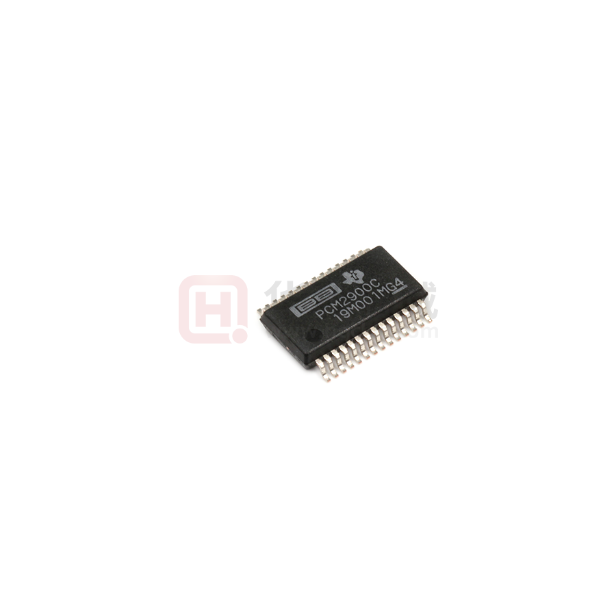
PCM2900C
PCM2902C
Burr-Brown Audio
SBFS039 – SEPTEMBER 2011
www.ti.com
Stereo Audio Codec with USB Interface,
Single-Ended Analog Input/Output, and S/PDIF
Check for Samples: PCM2900C, PCM2902C
FEATURES
1
• PCM2900C: Without S/PDIF
• PCM2902C: With S/PDIF
• On-Chip USB Interface:
– With Full-Speed Transceivers
– Fully Compliant with USB 2.0 Specification
– Certified by USB-IF
– Partially Programmable Descriptors
– USB Adaptive Mode for Playback
– USB Asynchronous Mode for Record
– Bus Powered
• 16-Bit Delta-Sigma ADC and DAC
• Sampling Rate:
– DAC: 32 kHz, 44.1 kHz, 48 kHz
– ADC: 8 kHz, 11.025 kHz, 16 kHz, 22.05 kHz,
32 kHz, 44.1 kHz, 48 kHz
• On-Chip Clock Generator with Single 12-MHz
Clock Source
• Single Power Supply:
– 5 V Typical (VBUS)
• Stereo ADC:
– Analog Performance at VBUS = 5 V:
– THD+N = 0.01%
– SNR = 89 dB
– Dynamic Range = 89 dB
– Decimation Digital Filter:
– Passband Ripple = ±0.05 dB
– Stop Band Attenuation = –65 dB
– Single-Ended Voltage Input
– Antialiasing Filter Included
– Digital HPF Included
•
234
•
•
Stereo DAC:
– Analog Performance at VBUS = 5 V:
– THD+N = 0.005%
– SNR = 96 dB
– Dynamic Range = 93 dB
– Oversampling Digital Filter:
– Passband Ripple = ±0.1 dB
– Stop Band Attenuation = –43 dB
– Single-Ended Voltage Output
– Analog LPF Included
Multifunctions:
– Human Interface Device (HID) Function:
– Volume and Mute Controls
– Suspend Flag Function
28-Pin SSOP Package
APPLICATIONS
•
•
•
•
USB Audio Speaker
USB Headset
USB Monitor
USB Audio Interface Box
DESCRIPTION
The PCM2900C/2902C are Texas Instruments'
single-chip, USB, stereo audio codecs with a
USB-compliant full-speed protocol controller and
S/PDIF (PCM2902C only). The USB protocol
controller requires no software code. The
PCM2900C/2902C employ SpAct™ architecture, TI's
unique system that recovers the audio clock from
USB packet data. On-chip analog PLLs with SpAct
architecture enable playback and record with low
clock jitter as well as independent playback and
record sampling rates.
1
2
3
4
Please be aware that an important notice concerning availability, standard warranty, and use in critical applications of Texas
Instruments semiconductor products and disclaimers thereto appears at the end of this data sheet.
SpAct is a trademark of Texas Instruments.
System Two, Audio Precision are trademarks of Audio Precision, Inc.
All other trademarks are the property of their respective owners.
PRODUCTION DATA information is current as of publication date.
Products conform to specifications per the terms of the Texas
Instruments standard warranty. Production processing does not
necessarily include testing of all parameters.
Copyright © 2011, Texas Instruments Incorporated
�PCM2900C
PCM2902C
SBFS039 – SEPTEMBER 2011
www.ti.com
This integrated circuit can be damaged by ESD. Texas Instruments recommends that all integrated circuits be handled with
appropriate precautions. Failure to observe proper handling and installation procedures can cause damage.
ESD damage can range from subtle performance degradation to complete device failure. Precision integrated circuits may be more
susceptible to damage because very small parametric changes could cause the device not to meet its published specifications.
PACKAGING/ORDERING INFORMATION (1)
SPECIFIED
TEMPERATURE
RANGE
PACKAGE
MARKING
PRODUCT
PACKAGE-LEAD
PACKAGE
DESIGNATOR
PCM2900CDB
SSOP-28
DB
–25°C to +85°C
PCM2900C
PCM2902CDB
SSOP-28
DB
–25°C to +85°C
PCM2902C
(1)
TRANSPORT
MEDIA,
QUANTITY
ORDERING
NUMBER
PCM2900CDB
Rails, 47
PCM2900CDBR
Tape and Reel,
2000
PCM2902CDB
Rails, 47
PCM2902CDBR
Tape and Reel,
2000
For the most current package and ordering information, see the Package Option Addendum at the end of this document, or see the
device product folder at www.ti.com.
ABSOLUTE MAXIMUM RATINGS (1)
Over operating free-air temperature range (unless otherwise noted).
PARAMETER
VBUS
PCM2900C/PCM2902C
UNIT
–0.3 to 6.5
V
Ground voltage differences, AGNDC, AGNDP, AGNDX, DGND, DGNDU
±0.1
V
SEL0, SEL1, TEST0 (DIN) (2)
–0.3 to 6.5
V
D+, D–, HID0, HID1, HID2, XTI, XTO, TEST1 (DOUT) (2), SSPND
–0.3 to (VDDI + 0.3) < 4
V
VINL, VINR, VCOM, VOUTR, VOUTL
–0.3 to (VCCCI + 0.3) < 4
V
VCCCI, VCCP1I, VCCP2I, VCCXI, VDDI
–0.3 to 4
V
±10
mA
Supply voltage
Digital input voltage
Analog input
voltage
Input current (any pins except supplies)
Ambient temperature under bias
–40 to +125
°C
Tstg
Storage temperature
–55 to +150
°C
TJ
Junction temperature
+150
°C
Package temperature (IR reflow, peak)
+250
°C
(1)
(2)
Stresses beyond those listed under Absolute Maximum Ratings may cause permanent damage to the device. These are stress ratings
only, and functional operation of the device at these or any other conditions beyond those indicated is not implied. Exposure to
absolute-maximum-rated conditions for extended periods may affect device reliability.
TEST0 and TEST1 apply to the PCM2900C; DIN and DOUT apply to the PCM2902C.
THERMAL INFORMATION
PCM2900C
THERMAL METRIC
(1)
PCM2902C
DB
DB
28 PINS
28 PINS
θJA
Junction-to-ambient thermal resistance
64.5
64.5
θJCtop
Junction-to-case (top) thermal resistance
24.5
24.5
θJB
Junction-to-board thermal resistance
25.4
25.4
ψJT
Junction-to-top characterization parameter
2.0
2.0
ψJB
Junction-to-board characterization parameter
25.0
25.0
θJCbot
Junction-to-case (bottom) thermal resistance
N/A
N/A
(1)
2
UNITS
°C/W
For more information about traditional and new thermal metrics, see the IC Package Thermal Metrics application report, SPRA953.
Submit Documentation Feedback
Copyright © 2011, Texas Instruments Incorporated
Product Folder Link(s): PCM2900C PCM2902C
�PCM2900C
PCM2902C
SBFS039 – SEPTEMBER 2011
www.ti.com
ELECTRICAL CHARACTERISTICS
All specifications at TA = +25°C, VBUS = 5 V, fS = 44.1 kHz, fIN = 1 kHz, and 16-bit data, unless otherwise noted.
PCM2900C, PCM2902C
PARAMETER
TEST CONDITIONS
MIN
TYP
MAX
UNIT
2
3.3
VDC
2.52
3.3
VDC
2
5.25
VDC
2.52
5.25
VDC
D+, D–
0.8
VDC
XTI, HID0, HID1,
and HID2
0.9
VDC
SEL0, SEL1
0.8
VDC
DIN (PCM2902C)
0.9
VDC
D+, D–, XTI, SEL0,
SEL1
±10
μA
50
80
μA
65
100
μA
±10
μA
±10
μA
±10
μA
DIGITAL INPUT/OUTPUT
Host interface
Apply USB Revision 2.0, full speed
Audio data format
USB isochronous data format
INPUT LOGIC
D+, D–
VIH
High-level input
voltage
XTI, HID0, HID1,
and HID2
SEL0, SEL1
DIN (PCM2902C)
VIL
IIH
Low-level input
voltage
High-level input
voltage
HID0, HID1, and
HID2
VIN = 3.3 V
DIN (PCM2902C)
D+, D–, XTI, SEL0,
SEL1
IIL
Low-level input
voltage
HID0, HID1, and
HID2
VIN = 0 V
DIN (PCM2902C)
OUTPUT LOGIC
D+, D–
VOH
High-level
output voltage
DOUT
(PCM2902C)
SSPND
2.8
VDC
IOH = –4 mA
2.8
VDC
IOH = –2 mA
2.8
VDC
D+, D–
VOL
Low-level output DOUT
voltage
(PCM2902C)
SSPND
0.3
VDC
IOL = 4 mA
0.5
VDC
IOL = 2 mA
0.5
VDC
12.008
MHz
CLOCK FREQUENCY
Input clock frequency, XTI
11.994
12
Submit Documentation Feedback
Copyright © 2011, Texas Instruments Incorporated
Product Folder Link(s): PCM2900C PCM2902C
3
�PCM2900C
PCM2902C
SBFS039 – SEPTEMBER 2011
www.ti.com
ELECTRICAL CHARACTERISTICS (continued)
All specifications at TA = +25°C, VBUS = 5 V, fS = 44.1 kHz, fIN = 1 kHz, and 16-bit data, unless otherwise noted.
PCM2900C, PCM2902C
PARAMETER
TEST CONDITIONS
MIN
TYP
MAX
UNIT
ADC CHARACTERISTICS
Resolution
Audio data channel
8, 16
Bits
1, 2
Channel
ADC Clock Frequency
fS
Sampling frequency
8, 11.025, 16, 22.05, 32, 44.1, 48
kHz
ADC DC Accuracy
Gain mismatch, channel-to-channel
±1
±5
% of
FSR
Gain error
±2
±10
% of
FSR
Bipolar zero error
±0
% of
FSR
ADC Dynamic Performance (1)
VIN = –1 dB (2), VCCCI = 3.67 V
THD+N
Total harmonic distortion plus noise
0.01
VIN = –1 dB (3)
VIN = –60 dB
SNR
0.02
0.1
%
%
5
%
Dynamic range
A-weighted
81
89
dB
Signal-to-noise ratio
A-weighted
81
89
dB
80
85
dB
Input voltage
0.6 VCCCI
VPP
Center voltage
0.5 VCCCI
Channel separation
Analog Input
Input impedance
Antialiasing filter frequency response
–3 dB
fIN = 20 kHz
V
30
kΩ
150
kHz
–0.08
dB
ADC Digital Filter Performance
Passband
0.454 fS
Stop band
0.583 fS
Hz
±0.05
Passband ripple
–65
Stop band attenuation
td
Delay time
HPF frequency response
(1)
(2)
(3)
4
dB
dB
17.4/fS
–3 dB
Hz
0.078 fS/1000
s
Hz
fIN = 1 kHz, using a System Two™ audio measurement system by Audio Precision™ in RMS mode with 20-kHz LPF, 400-Hz HPF in
calculation.
Using external voltage regulator for VCCCI (as shown in Table 7 and Figure 37, using with REG103xA-A).
Using internal voltage regulator for VCCCI (as shown in Figure 38 and Figure 39).
Submit Documentation Feedback
Copyright © 2011, Texas Instruments Incorporated
Product Folder Link(s): PCM2900C PCM2902C
�PCM2900C
PCM2902C
SBFS039 – SEPTEMBER 2011
www.ti.com
ELECTRICAL CHARACTERISTICS (continued)
All specifications at TA = +25°C, VBUS = 5 V, fS = 44.1 kHz, fIN = 1 kHz, and 16-bit data, unless otherwise noted.
PCM2900C, PCM2902C
PARAMETER
TEST CONDITIONS
MIN
TYP
MAX
UNIT
DAC CHARACTERISTICS
Resolution
Audio data channel
8, 16
Bits
1, 2
Channel
DAC Clock Frequency
fS
Sampling frequency
32, 44.1, 48
kHz
DAC DC Accuracy
Gain mismatch channel-to-channel
±1
±5
% of
FSR
Gain error
±2
±10
% of
FSR
Bipolar zero error
±2
% of
FSR
DAC Dynamic Performance (4)
THD+N
SNR
Total harmonic distortion plus noise
VOUT = 0 dB
0.005
VOUT = –60 dB
0.016
%
3
%
Dynamic range
EIAJ, A-weighted
87
93
dB
Signal-to-noise ratio
EIAJ, A-weighted
90
96
dB
86
92
dB
0.6 VCCCI
VPP
Channel separation
Analog Output
VO
Output voltage
Center voltage
Load impedance
LPF frequency response
0.5 VCCCI
AC coupling
V
10
–3 dB
f = 20 kHz
kΩ
250
kHz
–0.03
dB
DAC Digital Filter Performance
Passband
0.445 fS
Stop band
0.555 fS
Hz
±0.1
Passband ripple
–43
Stop band attenuation
td
Delay time
Hz
dB
dB
14.3 fS
s
POWER-SUPPLY REQUIREMENTS
VBUS
Voltage range
Supply current
PD
Power dissipation
VCCCI,
VCCP1I,
VCCP2I,
VCCXI,
VDDI
Internal power-supply voltage
4.35
ADC, DAC operation
Suspend mode
(5)
5
5.25
56
67
mA
352
mW
μA
250
ADC, DAC operation
280
Suspend mode (5)
1.25
3.1
3.3
VDC
mW
3.5
VDC
+85
°C
TEMPERATURE RANGE
–25
Operating temperature range
(4)
(5)
fOUT = 1 kHz, using a System Two audio measurement system by Audio Precision in RMS mode with 20-kHz LPF, 400-Hz HPF.
Under USB suspend state.
Submit Documentation Feedback
Copyright © 2011, Texas Instruments Incorporated
Product Folder Link(s): PCM2900C PCM2902C
5
�PCM2900C
PCM2902C
SBFS039 – SEPTEMBER 2011
www.ti.com
PCM2900C PIN ASSIGNMENTS
DB PACKAGE
SSOP-28
(TOP VIEW)
D+
1
28
D-
2
27
SSPND
VDDI
VBUS
3
26
DGND
DGNDU
4
25
TEST1
HID0
5
24
HID1
6
23
TEST0
VCCXI
HID2
7
SEL0
8
22
AGNDX
21
XTI
PCM2900C
SEL1
9
20
XTO
VCCCI
10
19
VCCP2I
AGNDC
11
18
VINL
12
17
AGNDP
VCCP1I
VINR
13
16
VOUTL
VCOM
14
15
VOUTR
Table 1. PCM2900C TERMINAL FUNCTIONS
TERMINAL
NAME
NO.
I/O
AGNDC
11
–
Analog ground for codec
AGNDP
18
–
Analog ground for PLL
AGNDX
22
–
Analog ground for oscillator
D–
2
I/O
USB differential input/output minus (1)
D+
1
I/O
USB differential input/output plus (1)
DGND
26
–
Digital ground
DGNDU
4
–
Digital ground for USB transceiver
HID0
5
I
HID key state input (mute), active-high (2)
HID1
6
I
HID key state input (volume up), active-high (2)
HID2
7
I
HID key state input (volume down), active-high (2)
SEL0
8
I
Must be set to high (3)
SEL1
9
I
Must be set to high (3)
SSPND
28
O
Suspend flag, active-low (low: suspend, high: operational)
TEST0
24
I
Test pin, must be connected to GND
TEST1
25
O
Test pin, must be left open
VBUS
3
–
Connect to USB power (VBUS)
VCCCI
10
–
Internal analog power supply for codec (4)
VCCP1I
17
–
Internal analog power supply for PLL (4)
VCCP2I
19
–
Internal analog power supply for PLL (4)
VCCXI
23
–
Internal analog power supply for oscillator (4)
VCOM
14
–
Common for ADC/DAC (VCCCI/2) (4)
VDDI
27
–
Internal digital power supply (4)
VINL
12
I
ADC analog input for L-channel
VINR
13
I
ADC analog input for R-channel
VOUTL
16
O
DAC analog output for L-channel
VOUTR
15
O
DAC analog output for R-channel
XTI
21
I
Crystal oscillator input
XTO
20
O
Crystal oscillator output
(1)
(2)
(3)
(4)
(5)
6
DESCRIPTION
(5)
LV-TTL level.
3.3-V CMOS-level input with internal pull-down. This pin informs the PC of serviceable control signals such as mute, volume up, or
volume down, which have no connection with the internal DAC or ADC directly. See the Interface #3 and End-Points sections.
TTL Schmitt trigger, 5-V tolerant.
Connect a decoupling capacitor to GND.
3.3-V, CMOS-level input.
Submit Documentation Feedback
Copyright © 2011, Texas Instruments Incorporated
Product Folder Link(s): PCM2900C PCM2902C
�PCM2900C
PCM2902C
SBFS039 – SEPTEMBER 2011
www.ti.com
PCM2902C PIN ASSIGNMENTS
DB PACKAGE
SSOP-28
(TOP VIEW)
D+
1
28
D-
2
27
SSPND
VDDI
VBUS
3
26
DGND
DGNDU
4
25
DOUT
HID0
5
24
HID1
6
23
DIN
VCCXI
HID2
7
SEL0
8
22
AGNDX
21
XTI
PCM2902C
SEL1
9
20
XTO
VCCCI
10
19
VCCP2I
AGNDC
11
18
VINL
12
17
AGNDP
VCCP1I
VINR
13
16
VOUTL
VCOM
14
15
VOUTR
Table 2. PCM2902C TERMINAL FUNCTIONS
TERMINAL
NAME
NO.
I/O
AGNDC
11
–
Analog ground for codec
AGNDP
18
–
Analog ground for PLL
AGNDX
22
–
Analog ground for oscillator
D–
2
I/O
USB differential input/output minus (1)
D+
1
I/O
USB differential input/output plus (1)
DGND
26
–
Digital ground
DGNDU
4
–
Digital ground for USB transceiver
DIN
24
I
S/PDIF input (2)
DOUT
25
O
S/PDIF output
HID0
5
I
HID key state input (mute), active high (3)
HID1
6
I
HID key state input (volume up), active high (3)
HID2
7
I
HID key state input (volume down), active high (3)
SEL0
8
I
Must be set to high (4)
SEL1
9
I
Must be set to high (4)
SSPND
28
O
Suspend flag, active-low (low: suspend, high: operational)
VBUS
3
–
Connect to USB power (VBUS)
VCCCI
10
–
Internal analog power supply for codec (5)
VCCP1I
17
–
Internal analog power supply for PLL (5)
VCCP2I
19
–
Internal analog power supply for PLL (5)
VCCXI
23
–
Internal analog power supply for oscillator (5)
VCOM
14
–
Common for ADC/DAC (VCCCI/2) (5)
VDDI
27
–
Internal digital power supply
VINL
12
I
ADC analog input for L-channel
VINR
13
I
ADC analog input for R-channel
VOUTL
16
O
DAC analog output for L-channel
VOUTR
15
O
DAC analog output for R-channel
XTI
21
I
Crystal oscillator input (6)
XTO
20
O
Crystal oscillator output
(1)
(2)
(3)
(4)
(5)
(6)
DESCRIPTION
LV-TTL level.
3.3-V CMOS-level input with internal pull-down, 5-V tolerant.
3.3-V CMOS-level input with internal pull-down. This pin informs the PC of serviceable control signals such as mute, volume up, or
volume down, which have no connection with the internal DAC or ADC directly. See the Interface #3 and End-Points sections.
TTL Schmitt trigger, 5-V tolerant.
Connect a decoupling capacitor to GND.
3.3-V, CMOS-level input.
Submit Documentation Feedback
Copyright © 2011, Texas Instruments Incorporated
Product Folder Link(s): PCM2900C PCM2902C
7
�PCM2900C
PCM2902C
SBFS039 – SEPTEMBER 2011
www.ti.com
PCM2900C FUNCTIONAL BLOCK DIAGRAM
VCCCI
VCCP1I
VCCP2I
VCCXI
VDDI
AGNDC
AGNDP
AGNDX
DGND
DGNDU
5-V to 3.3-V Voltage Regulator
Power
Manager
TEST0
SSPND
TEST1
VBUS
VINL
ISO-In
End-Point
USB SIE
VINR
Analog
PLL
VCOM
Selector
Analog
PLL
XCVR
FIFO
ADC
D+
D-
Control
End-Point
SEL0
SEL1
VOUTL
FIFO
DAC
VOUTR
ISO-Out
End-Point
HID
End-Point
HID0
HID1
HID2
USB
Protocol
Controller
96 MHz
PLL (×8)
XTI
8
12 MHz
Tracker
(SpAct)
XTO
Submit Documentation Feedback
Copyright © 2011, Texas Instruments Incorporated
Product Folder Link(s): PCM2900C PCM2902C
�PCM2900C
PCM2902C
SBFS039 – SEPTEMBER 2011
www.ti.com
PCM2902C FUNCTIONAL BLOCK DIAGRAM
VCCCI
VCCP1I
VCCP2I
VCCXI
VDDI
AGNDC
AGNDP
AGNDX
DGND
DGNDU
5-V to 3.3-V Voltage Regulator
Lock
DIN
Power
Manager
SSPND
S/PDIF Decoder
VBUS
VINL
ISO-In
End-Point
USB SIE
VINR
Analog
PLL
VCOM
Selector
Analog
PLL
XCVR
FIFO
ADC
D+
D-
Control
End-Point
SEL0
SEL1
VOUTL
FIFO
DAC
VOUTR
DOUT
ISO-Out
End-Point
HID
End-Point
S/PDIF Encoder
HID0
HID1
HID2
USB
Protocol
Controller
96 MHz
PLL (×8)
XTI
12 MHz
Tracker
(SpAct)
XTO
Submit Documentation Feedback
Copyright © 2011, Texas Instruments Incorporated
Product Folder Link(s): PCM2900C PCM2902C
9
�PCM2900C
PCM2902C
SBFS039 – SEPTEMBER 2011
www.ti.com
PCM2900C/2902C DIAGRAM OF ANALOG FRONT-END (RIGHT CHANNEL)
4.7 mF
+
VINR
30 kW
–
13
–
+
(+)
+
(–)
Delta-Sigma
Modulator
VCOM
14
+
(VCCCI/2)
10 mF
10
Reference
Submit Documentation Feedback
Copyright © 2011, Texas Instruments Incorporated
Product Folder Link(s): PCM2900C PCM2902C
�PCM2900C
PCM2902C
SBFS039 – SEPTEMBER 2011
www.ti.com
TYPICAL CHARACTERISTICS: ADC
All specifications at TA = +25°C, VBUS = 5 V, fS = 44.1 kHz, fin = 1 kHz, 16-bit data, using REG 103xA-A, unless otherwise
noted.
TOTAL HARMONIC DISTORTION + NOISE at –1 dB
vs FREE-AIR TEMPERATURE
DYNAMIC RANGE and SNR
vs FREE-AIR TEMPERATURE
95
Dynamic Range and SNR (dB)
Total Harmonic Distortion + Noise (%)
0.01
0.009
0.008
0.007
0.006
0.005
0.004
-50
0
-25
25
75
50
Free-Air Temperature (°C)
85
80
100
-50
0
-25
25
75
50
100
Free-Air Temperature (°C)
G001
G002
Figure 1.
Figure 2.
TOTAL HARMONIC DISTORTION + NOISE at –1 dB
vs SUPPLY VOLTAGE
DYNAMIC RANGE and SNR
vs SUPPLY VOLTAGE
95
Dynamic Range and SNR (dB)
0.01
Total Harmonic Distortion + Noise (%)
SNR
75
0.003
0.009
0.008
0.007
0.006
0.005
0.004
Dynamic Range
90
SNR
85
80
75
0.003
4
4.5
5
4
5.5
Supply Voltage (V)
4.5
5
5.5
Supply Voltage (V)
G003
G004
Figure 3.
Figure 4.
TOTAL HARMONIC DISTORTION + NOISE at –1 dB
vs SAMPLING FREQUENCY
DYNAMIC RANGE AND SNR
vs SAMPLING FREQUENCY
0.01
95
Dynamic Range and SNR (dB)
Total Harmonic Distortion + Noise (%)
Dynamic Range
90
0.009
0.008
0.007
0.006
0.005
0.004
0.003
Dynamic Range
90
SNR
85
80
75
30
35
40
45
Sampling Frequency (kHz)
50
30
G005
Figure 5.
35
40
45
Sampling Frequency (kHz)
50
G006
Figure 6.
Submit Documentation Feedback
Copyright © 2011, Texas Instruments Incorporated
Product Folder Link(s): PCM2900C PCM2902C
11
�PCM2900C
PCM2902C
SBFS039 – SEPTEMBER 2011
www.ti.com
TYPICAL CHARACTERISTICS: DAC
All specifications at TA = +25°C, VBUS = 5 V, fS = 44.1 kHz, fin = 1 kHz, 16-bit data, using REG 103xA-A, unless otherwise
noted.
TOTAL HARMONIC DISTORTION + NOISE at 0 dB
vs FREE-AIR TEMPERATURE
DYNAMIC RANGE AND SNR
vs FREE-AIR TEMPERATURE
98
Dynamic Range and SNR (dB)
Total Harmonic Distortion + Noise (%)
0.008
0.007
0.006
0.005
0.004
-50
0
-25
25
75
50
Free-Air Temperature (°C)
95
94
93
Dynamic Range
92
91
100
-50
0
-25
75
50
G007
100
G008
Figure 7.
Figure 8.
TOTAL HARMONIC DISTORTION + NOISE at 0 dB
vs SUPPLY VOLTAGE
DYNAMIC RANGE AND SNR
vs SUPPLY VOLTAGE
Dynamic Range and SNR (dB)
98
0.007
0.006
0.005
0.004
97
SNR
96
95
Dynamic Range
94
93
92
91
90
0.003
4
4.5
5
5.5
Supply Voltage (V)
4
4.5
5
5.5
Supply Voltage (V)
G009
G010
Figure 9.
Figure 10.
TOTAL HARMONIC DISTORTION + NOISE at 0 dB
vs SAMPLING FREQUENCY
DYNAMIC RANGE AND SNR
vs SAMPLING FREQUENCY
98
Dynamic Range and SNR (dB)
0.008
0.007
0.006
0.005
0.004
97
SNR
96
95
94
93
Dynamic Range
92
91
90
0.003
30
35
45
40
Sampling Frequency (kHz)
50
30
35
G011
Figure 11.
12
25
Free-Air Temperature (°C)
0.008
Total Harmonic Distortion + Noise (%)
SNR
96
90
0.003
Total Harmonic Distortion + Noise (%)
97
40
Sampling Frequency (kHz)
45
50
G012
Figure 12.
Submit Documentation Feedback
Copyright © 2011, Texas Instruments Incorporated
Product Folder Link(s): PCM2900C PCM2902C
�PCM2900C
PCM2902C
SBFS039 – SEPTEMBER 2011
www.ti.com
TYPICAL CHARACTERISTICS: SUPPLY CURRENT
All specifications at TA = +25°C, VBUS = 5 V, fS = 44.1 kHz, fin = 1 kHz, 16-bit data, using REG 103xA-A, unless otherwise
noted.
OPERATIONAL AND SUSPEND SUPPLY CURRENT
vs SUPPLY VOLTAGE
0.3
0.28
Operational
50
0.26
Suspend
40
0.24
30
0.22
20
Operational Supply Current (mA)
60
70
Suspend Supply Current (mA)
Operational Supply Current (mA)
70
OPERATIONAL SUPPLY CURRENT
vs SAMPLING FREQUENCY
0.2
4
4.25
4.5
5
4.75
60
50
ADC and DAC
40
30
20
5.5
5.25
Supply Voltage (V)
30
35
40
45
50
Sampling Frequency (kHz)
G013
Figure 13.
G014
Figure 14.
SUSPEND SUPPLY CURRENT
vs FREE-AIR TEMPERATURE
Suspend Supply Current (mA)
0.4
0.35
USB Spec Limit for Device (0.3 mA)
0.3
0.25
0.2
0.15
0.1
-40
-20
0
20
40
60
80
Free-Air Temperature (°C)
100
G015
Figure 15.
Submit Documentation Feedback
Copyright © 2011, Texas Instruments Incorporated
Product Folder Link(s): PCM2900C PCM2902C
13
�PCM2900C
PCM2902C
SBFS039 – SEPTEMBER 2011
www.ti.com
TYPICAL CHARACTERISTICS: ADC DIGITAL DECIMATION FILTER FREQUENCY RESPONSE
All specifications at TA = +25°C, VBUS = 5 V, fS = 44.1 kHz, fin = 1 kHz, 16-bit data, unless otherwise noted.
OVERALL CHARACTERISTICS
STOP BAND ATTENUATION
0
0
-10
-20
-20
Amplitude (dB)
Amplitude (dB)
-40
-60
-80
-100
-120
-40
-50
-60
-70
-80
-140
-90
-160
-100
0
16
8
24
0
32
Frequency (× fS)
0.2
0.4
0.6
0.8
G016
G017
Figure 16.
Figure 17.
PASSBAND RIPPLE
TRANSITION-BAND RESPONSE
0.2
0
0
-4
-0.2
-0.4
1
Frequency (× fS)
Amplitude (dB)
Amplitude (dB)
-30
-0.6
-8
-12
-16
-0.8
0
0.1
0.2
0.3
0.4
Frequency (× fS)
-20
0.46
0.5
0.48
0.5
0.52
0.54
Frequency (× fS)
G018
Figure 18.
G019
Figure 19.
TYPICAL CHARACTERISTICS: ADC DIGITAL HIGH-PASS FILTER FREQUENCY RESPONSE
All specifications at TA = +25°C, VBUS = 5 V, fS = 44.1 kHz, fin = 1 kHz, 16-bit data, unless otherwise noted.
STOP BAND CHARACTERISTICS
PASSBAND CHARACTERISTICS
0
0
-10
-0.2
-30
Amplitude (dB)
Amplitude (dB)
-20
-40
-50
-60
-70
-80
-0.4
-0.6
-0.8
-90
-100
-1.0
0
0.1
0.2
0.3
Frequency (× fS/1000)
0.4
0
G020
Figure 20.
14
1
2
Frequency (× fS/1000)
3
4
G021
Figure 21.
Submit Documentation Feedback
Copyright © 2011, Texas Instruments Incorporated
Product Folder Link(s): PCM2900C PCM2902C
�PCM2900C
PCM2902C
SBFS039 – SEPTEMBER 2011
www.ti.com
TYPICAL CHARACTERISTICS: ADC ANALOG ANTIALIASING FILTER FREQUENCY RESPONSE
All specifications at TA = +25°C, VBUS = 5 V, fS = 44.1 kHz, fin = 1 kHz, 16-bit data, unless otherwise noted.
PASSBAND CHARACTERISTICS
0
-10
-0.2
Amplitude (dB)
Amplitude (dB)
STOP BAND CHARACTERISTICS
0
-20
-30
-40
-0.4
-0.6
-0.8
-50
-1.0
1
10
100
1k
0.01
10k
0.1
1
10
100
Frequency (kHz)
Frequency (kHz)
G023
G022
Figure 22.
Figure 23.
TYPICAL CHARACTERISTICS: DAC DIGITAL INTERPOLATION FILTER FREQUENCY
RESPONSE
All specifications at TA = +25°C, VBUS = 5 V, fS = 44.1 kHz, fin = 1 kHz, 16-bit data, unless otherwise noted.
STOP BAND ATTENUATION
PASSBAND RIPPLE
0
0.2
-10
0
-30
Amplitude (dB)
Amplitude (dB)
-20
-40
-50
-60
-70
-80
-0.2
-0.4
-0.6
-90
-100
-0.8
0
1
2
4
3
Frequency (× fS)
0
0.1
0.2
0.3
0.4
0.5
Frequency (× fS)
G024
Figure 24.
G025
Figure 25.
TRANSITION-BAND RESPONSE
0
-2
Amplitude (dB)
-4
-6
-8
-10
-12
-14
-16
-18
-20
0.46
0.47
0.48
0.49
0.5
0.51
0.52
0.53
Frequency (× fS)
0.54
G026
Figure 26.
Submit Documentation Feedback
Copyright © 2011, Texas Instruments Incorporated
Product Folder Link(s): PCM2900C PCM2902C
15
�PCM2900C
PCM2902C
SBFS039 – SEPTEMBER 2011
www.ti.com
TYPICAL CHARACTERISTICS: DAC ANALOG FIR FILTER FREQUENCY RESPONSE
All specifications at TA = +25°C, VBUS = 5 V, fS = 44.1 kHz, fin = 1 kHz, 16-bit data, unless otherwise noted.
PASSBAND CHARACTERISTICS
0.2
-10
0
Amplitude (dB)
Amplitude (dB)
STOP BAND CHARACTERISTICS
0
-20
-30
-40
-0.2
-0.4
-0.6
-50
-0.8
0
8
16
24
Frequency (× fS)
32
0
0.1
0.2
0.3
0.4
Frequency (× fS)
G027
Figure 27.
0.5
G028
Figure 28.
TYPICAL CHARACTERISTICS: DAC ANALOG LOW-PASS FILTER FREQUENCY RESPONSE
All specifications at TA = +25°C, VBUS = 5 V, fS = 44.1 kHz, fin = 1 kHz, 16-bit data, unless otherwise noted.
PASSBAND CHARACTERISTICS
0
-10
-0.2
Amplitude (dB)
Amplitude (dB)
STOP BAND CHARACTERISTICS
0
-20
-30
-40
-0.4
-0.6
-0.8
-50
-1.0
1
10
100
1k
10k
0.01
0.1
1
100
G030
G029
Figure 29.
16
10
Frequency (kHz)
Frequency (kHz)
Figure 30.
Submit Documentation Feedback
Copyright © 2011, Texas Instruments Incorporated
Product Folder Link(s): PCM2900C PCM2902C
�PCM2900C
PCM2902C
SBFS039 – SEPTEMBER 2011
www.ti.com
DETAILED DESCRIPTION
USB INTERFACE
Control data and audio data are transferred to the PCM2900C/2902C via D+ (pin 1) and D– (pin 2). All data
to/from the PCM2900C/2902C are transferred at full speed. The device descriptor contains the information
described in Table 3.
Table 3. Device Description
USB revision
2.0 compliant
Device class
0x00 (device-defined interface level)
Device subclass
0x00 (not specified)
Device protocol
0x00 (not specified)
Max packet size for end-point 0
8 bytes
Vendor ID
0x08BB
Product ID
0x29C0 / 0x29C2
Device release number
1.0 (0x0100)
Number of configurations
1
Vendor strings
String #1 (see Table 5)
Product strings
String #2 (see Table 5)
Serial number
Not supported
The configuration descriptor contains the information described in Table 4.
Table 4. Configuration Descriptor
Interface
Four interfaces
Power attribute
0x80 (Bus-powered, no remote
wakeup)
Max power
0x32 (100 mA)
The string descriptor contains the information described in Table 5.
Table 5. String Descriptor
#0
0x0409
#1
BurrBrown from Texas Instruments
#2
USB AUDIO CODEC
Submit Documentation Feedback
Copyright © 2011, Texas Instruments Incorporated
Product Folder Link(s): PCM2900C PCM2902C
17
�PCM2900C
PCM2902C
SBFS039 – SEPTEMBER 2011
www.ti.com
DEVICE CONFIGURATION
Figure 31 illustrates the USB audio function topology. The PCM2900C/2902C has four interfaces. Each interface
consists of alternative settings.
End-Point #0
Default End-Point
FU
End-Point #2
(IF #1)
Analog Out
IT
TID1
OT
TID2
Audio Streaming Interface
UID3
End-Point #4
(IF #2)
Analog In
IT
TID4
OT
TID5
Audio Streaming Interface
Standard Audio Control Interface (IF #0)
End-Point #5
(IF #3)
HID Interface
Figure 31. USB Audio Function Topology
18
Submit Documentation Feedback
Copyright © 2011, Texas Instruments Incorporated
Product Folder Link(s): PCM2900C PCM2902C
�PCM2900C
PCM2902C
SBFS039 – SEPTEMBER 2011
www.ti.com
Interface #0
Interface #0 is defined as the control interface. Alternative setting #0 is the only possible setting for interface #0.
Alternative setting #0 describes the standard audio control interface. The audio control interface consists of a
single terminal. The PCM2900C/2902C has five terminals:
• Input terminal (IT #1) for isochronous-out stream
• Output terminal (OT #2) for audio analog output
• Feature unit (FU #3) for DAC digital attenuator
• Input terminal (IT #4) for audio analog input
• Output terminal (OT #5) for isochronous-in stream
Input terminal #1 is defined as a USB stream (terminal type 0x0101). Input terminal #1 can accept two-channel
audio streams consisting of left and right channels. Output terminal #2 is defined as a speaker (terminal type
0x0301). Input terminal #4 is defined as a line connector (terminal type 0x0603). Output terminal #5 is defined as
a USB stream (terminal type 0x0101). Output terminal #5 can generate two-channel audio streams composed of
left and right channel data. Feature unit #3 supports the following sound control features:
• Volume control
• Mute control
The built-in digital volume controller can be manipulated by an audio class specific request from 0 dB to –64 dB
in 1-dB steps. Changes are made by incrementing or decrementing by one step (1 dB) for every 1/fS time interval
until the volume level has reached the requested value. Each channel can be set for different values. The master
volume control is not supported. A request to the master volume is stalled and ignored. The built-in digital mute
controller can be manipulated by an audio class specific request. A master mute control request is acceptable. A
request to an individual channel is stalled and ignored.
Interface #1
Interface #1 is the audio streaming data-out interface. Interface #1 has five alternative settings listed in Table 6.
Alternative setting #0 is the zero bandwidth setting. All other alternative settings are operational settings.
Table 6. Interface #1 Alternative Settings
ALTERNATIVE
SETTING
DATA FORMAT
00
TRANSFER
MODE
SAMPLING RATE
(kHz)
Zero Bandwidth
01
16-bit
Stereo
Twos complement (PCM)
Adaptive
32, 44.1, 48
02
03
16-bit
Mono
Twos complement (PCM)
Adaptive
32, 44.1, 48
8-bit
Stereo
Twos complement (PCM)
Adaptive
04
32, 44.1, 48
8-bit
Mono
Twos complement (PCM)
Adaptive
32, 44.1, 48
Submit Documentation Feedback
Copyright © 2011, Texas Instruments Incorporated
Product Folder Link(s): PCM2900C PCM2902C
19
�PCM2900C
PCM2902C
SBFS039 – SEPTEMBER 2011
www.ti.com
Interface #2
Interface #2 is the audio streaming data-in interface. Interface #2 has the 19 alternative settings listed in Table 7.
Alternative setting #0 is the zero bandwidth setting. All other alternative settings are operational settings.
Table 7. Interface #2 Alternative Settings
ALTERNATIVE
SETTING
DATA FORMAT
00
TRANSFER
MODE
SAMPLING RATE
(kHz)
48
Zero Bandwidth
01
16-bit
Stereo
Twos complement (PCM)
Asynchronous
02
03
16-bit
Mono
Twos complement (PCM)
Asynchronous
48
16-bit
Stereo
Twos complement (PCM)
Asynchronous
44.1
04
05
16-bit
Mono
Twos complement (PCM)
Asynchronous
44.1
16-bit
Stereo
Twos complement (PCM)
Asynchronous
32
06
07
16-bit
Mono
Twos complement (PCM)
Asynchronous
32
16-bit
Stereo
Twos complement (PCM)
Asynchronous
22.05
08
16-bit
Mono
Twos complement (PCM)
Asynchronous
22.05
09
16-bit
Stereo
Twos complement (PCM)
Asynchronous
16
0A
16-bit
Mono
Twos complement (PCM)
Asynchronous
16
0B
8-bit
Stereo
Twos complement (PCM)
Asynchronous
16
0C
8-bit
Mono
Twos complement (PCM)
Asynchronous
16
0D
8-bit
Stereo
Twos complement (PCM)
Asynchronous
8
0E
8-bit
Mono
Twos complement (PCM)
Asynchronous
8
0F
16-bit
Stereo
Twos complement (PCM)
Synchronous
11.025
10
16-bit
Mono
Twos complement (PCM)
Synchronous
11.025
11
8-bit
Stereo
Twos complement (PCM)
Synchronous
11.025
12
8-bit
Mono
Twos complement (PCM)
Synchronous
11.025
Interface #3
Interface #3 is the interrupt data-in interface. Alternative setting #0 is the only possible setting for interface #3.
Interface #3 consists of the HID consumer control device and reports the status of three key parameters:
• Mute (0xE209)
• Volume up (0xE909)
• Volume down (0xEA09)
End-Points
The PCM2900C/2902C has the following four end-points:
• Control end-point (EP #0)
• Isochronous-out audio data stream end-point (EP #2)
• Isochronous-in audio data stream end-point (EP #4)
• HID end-point (EP #5)
The control end-point is a default end-point. The control end-point is used to control all functions of the
PCM2900C/2902C by a standard USB request and an USB audio class-specific request from the host. The
isochronous-out audio data stream end-point is an audio sink end-point, which receives the PCM audio data. The
isochronous-out audio data stream end-point accepts the adaptive transfer mode. The isochronous-in audio data
stream end-point is an audio source end-point, which transmits the PCM audio data. The isochronous-in audio
data stream end-point uses asynchronous transfer mode. The HID end-point is an interrupt-in end-point. HID
end-point reports HID0, HID1, and HID2 pin status every 32 ms.
The human interface device (HID) pins are defined as consumer control devices. The HID function is designed
as an independent end-point from both isochronous-in and -out end-points. Therefore, the result obtained from
the HID operation depends on the host software. Typically, the HID function is used as the primary audio-out
device.
20
Submit Documentation Feedback
Copyright © 2011, Texas Instruments Incorporated
Product Folder Link(s): PCM2900C PCM2902C
�PCM2900C
PCM2902C
SBFS039 – SEPTEMBER 2011
www.ti.com
Clock and Reset
The PCM2900C/2902C requires a 12-MHz (±500 ppm) clock for the USB and audio functions, which can be
generated by a built-in crystal oscillator with a 12-MHz crystal resonator. The 12-MHz crystal resonator must be
connected to XTI (pin 21) and XTO (pin 20) with one high (1-MΩ) resistor and two small capacitors, the
capacitance of which depends on the load capacitance of the crystal resonator. The external clock can be
supplied from XTI (pin 21). If the external clock is supplied, XTO (pin 20) must be left open. Because there is no
clock-disabling signal, it is not recommended to use the external clock supply. SSPND (pin 28) is unable to use
clock disabling.
The PCM2900C/2902C has an internal power-on reset circuit, which triggers automatically when VBUS (pin 3)
exceeds 2.5 V typical (2.7 V to 2.2 V). Approximately 700 μs is required until internal reset release.
Digital Audio Interface (PCM2902C)
The PCM2902C employs both S/PDIF input and output. Isochronous-out data from the host are encoded to the
S/PDIF output and the DAC analog output. Input data are selected as either S/PDIF or ADC analog input. When
the device detects an S/PDIF input and successfully locks the received data, the isochronous-in transfer data
source is automatically selected from S/PDIF itself; otherwise, the data source is selected to ADC analog input.
This feature is a customer option. It is the responsibility of the user to implement this feature.
Supported Input/Output Data (PCM2902C)
The following data formats are accepted by the S/PDIF input and output. All other data formats are unable to use
S/PDIF.
• 48-kHz 16-bit stereo
• 44.1-kHz 16-bit stereo
• 32-kHz 16-bit stereo
Any mismatch of the sampling rate between the input S/PDIF signal and the host command is not acceptable.
Any mismatch of the data format between the input S/PDIF signal and the host command may cause unexpected
results, with the following exceptions:
• Recording in monaural format from stereo data input at the same data rate
• Recording in 8-bit format from 16-bit data input at the same data rate
A combination of these two conditions is not acceptable.
For playback, all possible data rate sources are converted to 16-bit stereo format at the same source data rate.
Channel Status Information (PCM2902C)
The channel status information is fixed as consumer application, PCM mode, copyright, and digital/digital
converter. All other bits are fixed as 0s except for the sample frequency, which is set automatically according to
the data received through the USB.
Copyright Management (PCM2902C)
Isochronous-in data are affected by the serial copy management system (SCMS). When receiving digital audio
data that are indicated as original data in the control bit, input digital audio data transfer to the host. If the data
are indicated as first generation or higher, the transferred data are routed to the analog input.
Digital audio data output is always encoded as original with SCMS control.
Submit Documentation Feedback
Copyright © 2011, Texas Instruments Incorporated
Product Folder Link(s): PCM2900C PCM2902C
21
�PCM2900C
PCM2902C
SBFS039 – SEPTEMBER 2011
www.ti.com
INTERFACE SEQUENCE
Power On, Attach, and Playback Sequence
The PCM2900C/2902C is ready for setup when the reset sequence has finished and the USB bus is attached.
After connection has been established by setup, the PCM2900C/2902C is ready to accept USB audio data.
While waiting, the audio data (idle state) and analog output are set to bipolar zero (BPZ).
When receiving the audio data, the PCM2900C/2902C stores the first audio packet, which contains 1-ms audio
data, into the internal storage buffer. The PCM2900C/2902C starts to play the audio data when detecting the
next start of frame (SOF) packet, as illustrated in Figure 32.
5 V (Typ)
VBUS (Pin 3)
2.5 V (Typ)
0V
Bus Reset
First Audio Data
Set Configuration
Second Audio Data
Bus Idle
D+/DSOF
SOF
SOF
SSPND
BPZ
VOUTL
VOUTR
700 ms
Device Setup
Internal Reset
Ready for Setup
1 ms
Ready for Playback
Figure 32. Initial Sequence
Play, Stop, and Detach Sequence
When the host finishes or aborts playback, the PCM2900C/2902C stops playing after the last audio data have
played, as shown in Figure 33.
VBUS (Pin 3)
Audio Data
Audio Data
Last Audio Data
D+/DSOF
SOF
SOF
SOF
SOF
VOUTL
VOUTR
Detach
1 ms
Figure 33. Play, Stop, and Detach Sequence
22
Submit Documentation Feedback
Copyright © 2011, Texas Instruments Incorporated
Product Folder Link(s): PCM2900C PCM2902C
�PCM2900C
PCM2902C
SBFS039 – SEPTEMBER 2011
www.ti.com
Record Sequence
The PCM2900C/2902C starts the audio capture into the internal memory after receiving the SET_INTERFACE
command, as shown in Figure 34.
Audio Data
SET_INTERFACE
IN Token
Audio Data
IN Token
Audio Data
IN Token
D+/DSOF
SOF
SOF
SOF
SOF
VINL
VINR
1 ms
Figure 34. Record Sequence
Suspend and Resume Sequence
The PCM2900C/2902C enters the suspend state after it sees a constant idle state on the USB bus
(approximately 5 ms), as shown in Figure 35. While the PCM2900C/2902C enters the suspend state, SSPND
flag (pin 28) is asserted. The PCM2900C/2902C wakes up immediately upon detecting a non-idle state on the
USB bus.
Idle
D+/D-
SSPND
Active
5 ms
Suspend
Active
Figure 35. Suspend and Resume Sequence
Submit Documentation Feedback
Copyright © 2011, Texas Instruments Incorporated
Product Folder Link(s): PCM2900C PCM2902C
23
�PCM2900C
PCM2902C
SBFS039 – SEPTEMBER 2011
www.ti.com
APPLICATION INFORMATION
PCM2900C TYPICAL CIRCUIT CONNECTION 1
Figure 36 illustrates a typical circuit connection for a high-performance application. The circuit illustrated is for
information only. The entire board design should be considered to meet the USB specification as a
USB-compliant product.
1.5 kW × 3
1.5 kW
PCM2900C
22 W
D+
1
D+
SSPND
28
2
D-
VDDI
27
3
VBUS
DGND
26
4
DGNDU
TEST1
25
5
HID0
TEST0
24
6
HID1
VCCXI
23
7
HID2
AGNDX
22
8
SEL0
XTI
21
9
SEL1
XTO
20
10
VCCCI
VCCP2I
19
11
AGNDC
AGNDP
18
12
VINL
VCCP1I
17
13
VINR
VOUTL
16
14
VCOM
VOUTR
15
22 W
D-
C3
2.2 W
VBUS
1 mF
GND
IC1
IN OUT GND ADJ EN
1
2
3
C13
4
5
D1
C10
+
27 kW
+
12 MHz
13 kW
+
C5
1 MW
C6
3.6 V to
3.85 V
C1
C9
C4
C2
+
C7
MUTE/
Power
Down
C8
+
C11
+
C12
LPF,
Amp
LPF,
Amp
NOTE: C1, C2: 10 μF
C3, C4, C7, C8, C13: 1 μF (These capacitors must be less than 2 μF.)
C5, C6: 10 pF to 33 pF (depending on crystal resonator)
C9, C10, C11, C12: The capacitance may vary depending on design.
IC1: REG103xA-A (TI) or equivalent. Analog performance may vary depending on IC1.
D1: Schottky barrier diode (VF ≤ 350 mV at 10 mA, IR ≤ 2 μA at 4 V)
Figure 36. Bus-Powered Configuration for High-Performance Application
24
Submit Documentation Feedback
Copyright © 2011, Texas Instruments Incorporated
Product Folder Link(s): PCM2900C PCM2902C
�PCM2900C
PCM2902C
SBFS039 – SEPTEMBER 2011
www.ti.com
PCM2902C TYPICAL CIRCUIT CONNECTION 1
Figure 37 illustrates a typical circuit connection for a high-performance application. The circuit illustrated is for
information only. The entire board design should be considered to meet the USB specification as a
USB-compliant product.
1.5 kW × 3
1.5 kW
PCM2902C
22 W
D+
1
D+
SSPND
28
2
D-
VDDI
27
3
VBUS
DGND
26
4
DGNDU
DOUT
25
5
HID0
DIN
24
6
HID1
VCCXI
23
7
HID2
AGNDX
22
8
SEL0
XTI
21
9
SEL1
XTO
20
10
VCCCI
VCCP2I
19
11
AGNDC
AGNDP
18
12
VINL
VCCP1I
17
13
VINR
VOUTL
16
14
VCOM
VOUTR
15
22 W
D-
C3
2.2 W
VBUS
1 mF
GND
IC1
IN OUT GND ADJ EN
1
2
3
C13
4
5
D1
C10
+
27 kW
+
12 MHz
13 kW
+
C5
1 MW
C6
3.6 V to
3.85 V
C1
C9
C4
C2
+
C7
MUTE/
Power
Down
C8
+
C11
+
C12
LPF,
Amp
LPF,
Amp
NOTE: C1, C2: 10 μF
C3, C4, C7, C8, C13: 1 μF (These capacitors must be less than 2 μF.)
C5, C6: 10 pF to 33 pF (depending on crystal resonator)
C9, C10, C11, C12: The capacitance may vary depending on design.
IC1: REG103xA-A (TI) or equivalent. Analog performance may vary depending on IC1.
D1: Schottky barrier diode (VF ≤ 350 mV at 10 mA, IR ≤ 2 μA at 4 V)
Figure 37. Bus-Powered Configuration for High-Performance Application
Submit Documentation Feedback
Copyright © 2011, Texas Instruments Incorporated
Product Folder Link(s): PCM2900C PCM2902C
25
�PCM2900C
PCM2902C
SBFS039 – SEPTEMBER 2011
www.ti.com
PCM2900C TYPICAL CIRCUIT CONNECTION 2
Figure 38 illustrates a typical circuit connection for a simple application. The circuit illustrated is for information
only. The entire board design should be considered to meet the USB specification as a USB-compliant product.
1.5 kW × 4
PCM2900C
22 W
D+
1
D+
SSPND
28
2
D-
VDDI
27
3
VBUS
DGND
26
4
DGNDU
TEST1
25
5
HID0
TEST0
24
6
HID1
VCCXI
23
7
HID2
AGNDX
22
8
SEL0
XTI
21
9
SEL1
XTO
20
10
VCCCI
VCCP2I
19
11
AGNDC
AGNDP
18
12
VINL
VCCP1I
17
13
VINR
VOUTL
16
14
VCOM
VOUTR
15
22 W
D-
C3
2.2 W
VBUS
1 mF
GND
C4
C5
1 MW
C6
12 MHz
C1
+
C9
C10
+
+
C2
+
C7
MUTE/
Power
Down
C8
+
C11
+
C12
LPF,
Amp
LPF,
Amp
NOTE: C1, C2: 10 μF
C3, C4, C7, C8: 1 μF (These capacitors must be less than 2 μF.)
C5, C6: 10 pF to 33 pF (depending on crystal resonator)
C9, C10, C11, C12: The capacitance may vary depending on design.
In this case, the analog performance of the ADC may be degraded.
Figure 38. Bus-Powered Configuration
26
Submit Documentation Feedback
Copyright © 2011, Texas Instruments Incorporated
Product Folder Link(s): PCM2900C PCM2902C
�PCM2900C
PCM2902C
SBFS039 – SEPTEMBER 2011
www.ti.com
PCM2902C TYPICAL CIRCUIT CONNECTION 2
Figure 39 illustrates a typical circuit connection for a simple application. The circuit illustrated is for information
only. The entire board design should be considered to meet the USB specification as a USB-compliant product.
1.5 kW × 4
PCM2902C
22 W
D+
1
D+
SSPND
28
2
D-
VDDI
27
3
VBUS
DGND
26
4
DGNDU
DOUT
25
5
HID0
DIN
24
6
HID1
VCCXI
23
7
HID2
AGNDX
22
8
SEL0
XTI
21
9
SEL1
XTO
20
10
VCCCI
VCCP2I
19
11
AGNDC
AGNDP
18
12
VINL
VCCP1I
17
13
VINR
VOUTL
16
14
VCOM
VOUTR
15
22 W
D-
C3
2.2 W
VBUS
1 mF
GND
C4
C5
1 MW
C6
12 MHz
C1
+
C9
C10
+
+
C2
+
C7
MUTE/
Power
Down
C8
+
C11
+
C12
LPF,
Amp
LPF,
Amp
NOTE: C1, C2: 10 μF
C3, C4, C7, C8: 1 μF (These capacitors must be less than 2 μF.)
C5, C6: 10 pF to 33 pF (depending on crystal resonator)
C9, C10, C11, C12: The capacitance may vary depending on design.
In this case, the analog performance of the ADC may be degraded.
Figure 39. Bus-Powered Configuration
OPERATING ENVIRONMENT
For current information on the PCM2900C/2902C operating environment, see the application report, Updated
Operating Environments for PCM270X, PCM290X Applications (SLAA374), available for download from the TI
website.
Submit Documentation Feedback
Copyright © 2011, Texas Instruments Incorporated
Product Folder Link(s): PCM2900C PCM2902C
27
�PACKAGE OPTION ADDENDUM
www.ti.com
11-Apr-2013
PACKAGING INFORMATION
Orderable Device
Status
(1)
Package Type Package Pins Package
Drawing
Qty
Eco Plan
Lead/Ball Finish
(2)
MSL Peak Temp
Op Temp (°C)
Top-Side Markings
(3)
(4)
PCM2900CDB
ACTIVE
SSOP
DB
28
50
Green (RoHS
& no Sb/Br)
CU NIPDAU
Level-1-260C-UNLIM
-25 to 85
PCM2900C
PCM2900CDBR
ACTIVE
SSOP
DB
28
2000
Green (RoHS
& no Sb/Br)
CU NIPDAU
Level-1-260C-UNLIM
-25 to 85
PCM2900C
PCM2902CDB
ACTIVE
SSOP
DB
28
50
Green (RoHS
& no Sb/Br)
CU NIPDAU
Level-1-260C-UNLIM
-25 to 85
PCM2902C
PCM2902CDBR
ACTIVE
SSOP
DB
28
2000
Green (RoHS
& no Sb/Br)
CU NIPDAU
Level-1-260C-UNLIM
-25 to 85
PCM2902C
(1)
The marketing status values are defined as follows:
ACTIVE: Product device recommended for new designs.
LIFEBUY: TI has announced that the device will be discontinued, and a lifetime-buy period is in effect.
NRND: Not recommended for new designs. Device is in production to support existing customers, but TI does not recommend using this part in a new design.
PREVIEW: Device has been announced but is not in production. Samples may or may not be available.
OBSOLETE: TI has discontinued the production of the device.
(2)
Eco Plan - The planned eco-friendly classification: Pb-Free (RoHS), Pb-Free (RoHS Exempt), or Green (RoHS & no Sb/Br) - please check http://www.ti.com/productcontent for the latest availability
information and additional product content details.
TBD: The Pb-Free/Green conversion plan has not been defined.
Pb-Free (RoHS): TI's terms "Lead-Free" or "Pb-Free" mean semiconductor products that are compatible with the current RoHS requirements for all 6 substances, including the requirement that
lead not exceed 0.1% by weight in homogeneous materials. Where designed to be soldered at high temperatures, TI Pb-Free products are suitable for use in specified lead-free processes.
Pb-Free (RoHS Exempt): This component has a RoHS exemption for either 1) lead-based flip-chip solder bumps used between the die and package, or 2) lead-based die adhesive used between
the die and leadframe. The component is otherwise considered Pb-Free (RoHS compatible) as defined above.
Green (RoHS & no Sb/Br): TI defines "Green" to mean Pb-Free (RoHS compatible), and free of Bromine (Br) and Antimony (Sb) based flame retardants (Br or Sb do not exceed 0.1% by weight
in homogeneous material)
(3)
MSL, Peak Temp. -- The Moisture Sensitivity Level rating according to the JEDEC industry standard classifications, and peak solder temperature.
(4)
Multiple Top-Side Markings will be inside parentheses. Only one Top-Side Marking contained in parentheses and separated by a "~" will appear on a device. If a line is indented then it is a
continuation of the previous line and the two combined represent the entire Top-Side Marking for that device.
Important Information and Disclaimer:The information provided on this page represents TI's knowledge and belief as of the date that it is provided. TI bases its knowledge and belief on information
provided by third parties, and makes no representation or warranty as to the accuracy of such information. Efforts are underway to better integrate information from third parties. TI has taken and
continues to take reasonable steps to provide representative and accurate information but may not have conducted destructive testing or chemical analysis on incoming materials and chemicals.
TI and TI suppliers consider certain information to be proprietary, and thus CAS numbers and other limited information may not be available for release.
In no event shall TI's liability arising out of such information exceed the total purchase price of the TI part(s) at issue in this document sold by TI to Customer on an annual basis.
Addendum-Page 1
Samples
�PACKAGE OPTION ADDENDUM
www.ti.com
11-Apr-2013
Addendum-Page 2
�PACKAGE MATERIALS INFORMATION
www.ti.com
26-Mar-2013
TAPE AND REEL INFORMATION
*All dimensions are nominal
Device
PCM2902CDBR
Package Package Pins
Type Drawing
SSOP
DB
28
SPQ
Reel
Reel
A0
Diameter Width (mm)
(mm) W1 (mm)
2000
330.0
16.4
Pack Materials-Page 1
8.2
B0
(mm)
K0
(mm)
P1
(mm)
W
Pin1
(mm) Quadrant
10.5
2.5
12.0
16.0
Q1
�PACKAGE MATERIALS INFORMATION
www.ti.com
26-Mar-2013
*All dimensions are nominal
Device
Package Type
Package Drawing
Pins
SPQ
Length (mm)
Width (mm)
Height (mm)
PCM2902CDBR
SSOP
DB
28
2000
367.0
367.0
38.0
Pack Materials-Page 2
�MECHANICAL DATA
MSSO002E – JANUARY 1995 – REVISED DECEMBER 2001
DB (R-PDSO-G**)
PLASTIC SMALL-OUTLINE
28 PINS SHOWN
0,38
0,22
0,65
28
0,15 M
15
0,25
0,09
8,20
7,40
5,60
5,00
Gage Plane
1
14
0,25
A
0°–ā8°
0,95
0,55
Seating Plane
2,00 MAX
0,10
0,05 MIN
PINS **
14
16
20
24
28
30
38
A MAX
6,50
6,50
7,50
8,50
10,50
10,50
12,90
A MIN
5,90
5,90
6,90
7,90
9,90
9,90
12,30
DIM
4040065 /E 12/01
NOTES: A.
B.
C.
D.
All linear dimensions are in millimeters.
This drawing is subject to change without notice.
Body dimensions do not include mold flash or protrusion not to exceed 0,15.
Falls within JEDEC MO-150
POST OFFICE BOX 655303
• DALLAS, TEXAS 75265
�IMPORTANT NOTICE
Texas Instruments Incorporated and its subsidiaries (TI) reserve the right to make corrections, enhancements, improvements and other
changes to its semiconductor products and services per JESD46, latest issue, and to discontinue any product or service per JESD48, latest
issue. Buyers should obtain the latest relevant information before placing orders and should verify that such information is current and
complete. All semiconductor products (also referred to herein as “components”) are sold subject to TI’s terms and conditions of sale
supplied at the time of order acknowledgment.
TI warrants performance of its components to the specifications applicable at the time of sale, in accordance with the warranty in TI’s terms
and conditions of sale of semiconductor products. Testing and other quality control techniques are used to the extent TI deems necessary
to support this warranty. Except where mandated by applicable law, testing of all parameters of each component is not necessarily
performed.
TI assumes no liability for applications assistance or the design of Buyers’ products. Buyers are responsible for their products and
applications using TI components. To minimize the risks associated with Buyers’ products and applications, Buyers should provide
adequate design and operating safeguards.
TI does not warrant or represent that any license, either express or implied, is granted under any patent right, copyright, mask work right, or
other intellectual property right relating to any combination, machine, or process in which TI components or services are used. Information
published by TI regarding third-party products or services does not constitute a license to use such products or services or a warranty or
endorsement thereof. Use of such information may require a license from a third party under the patents or other intellectual property of the
third party, or a license from TI under the patents or other intellectual property of TI.
Reproduction of significant portions of TI information in TI data books or data sheets is permissible only if reproduction is without alteration
and is accompanied by all associated warranties, conditions, limitations, and notices. TI is not responsible or liable for such altered
documentation. Information of third parties may be subject to additional restrictions.
Resale of TI components or services with statements different from or beyond the parameters stated by TI for that component or service
voids all express and any implied warranties for the associated TI component or service and is an unfair and deceptive business practice.
TI is not responsible or liable for any such statements.
Buyer acknowledges and agrees that it is solely responsible for compliance with all legal, regulatory and safety-related requirements
concerning its products, and any use of TI components in its applications, notwithstanding any applications-related information or support
that may be provided by TI. Buyer represents and agrees that it has all the necessary expertise to create and implement safeguards which
anticipate dangerous consequences of failures, monitor failures and their consequences, lessen the likelihood of failures that might cause
harm and take appropriate remedial actions. Buyer will fully indemnify TI and its representatives against any damages arising out of the use
of any TI components in safety-critical applications.
In some cases, TI components may be promoted specifically to facilitate safety-related applications. With such components, TI’s goal is to
help enable customers to design and create their own end-product solutions that meet applicable functional safety standards and
requirements. Nonetheless, such components are subject to these terms.
No TI components are authorized for use in FDA Class III (or similar life-critical medical equipment) unless authorized officers of the parties
have executed a special agreement specifically governing such use.
Only those TI components which TI has specifically designated as military grade or “enhanced plastic” are designed and intended for use in
military/aerospace applications or environments. Buyer acknowledges and agrees that any military or aerospace use of TI components
which have not been so designated is solely at the Buyer's risk, and that Buyer is solely responsible for compliance with all legal and
regulatory requirements in connection with such use.
TI has specifically designated certain components as meeting ISO/TS16949 requirements, mainly for automotive use. In any case of use of
non-designated products, TI will not be responsible for any failure to meet ISO/TS16949.
Products
Applications
Audio
www.ti.com/audio
Automotive and Transportation
www.ti.com/automotive
Amplifiers
amplifier.ti.com
Communications and Telecom
www.ti.com/communications
Data Converters
dataconverter.ti.com
Computers and Peripherals
www.ti.com/computers
DLP® Products
www.dlp.com
Consumer Electronics
www.ti.com/consumer-apps
DSP
dsp.ti.com
Energy and Lighting
www.ti.com/energy
Clocks and Timers
www.ti.com/clocks
Industrial
www.ti.com/industrial
Interface
interface.ti.com
Medical
www.ti.com/medical
Logic
logic.ti.com
Security
www.ti.com/security
Power Mgmt
power.ti.com
Space, Avionics and Defense
www.ti.com/space-avionics-defense
Microcontrollers
microcontroller.ti.com
Video and Imaging
www.ti.com/video
RFID
www.ti-rfid.com
OMAP Applications Processors
www.ti.com/omap
TI E2E Community
e2e.ti.com
Wireless Connectivity
www.ti.com/wirelessconnectivity
Mailing Address: Texas Instruments, Post Office Box 655303, Dallas, Texas 75265
Copyright © 2014, Texas Instruments Incorporated
�