Not Recommended for New Designs
�������
�� ��
�����
�
� � ��� ������� ���
PCM2900
PCM2902
SLES035E – MARCH 2007 – REVISED MARCH 2008
STEREO AUDIO CODEC WITH USB INTERFACE,
SINGLE-ENDED ANALOG INPUT/OUTPUT AND S/PDIF
FEATURES
1
• PCM2900: Without S/PDIF
• PCM2902: With S/PDIF
• On-Chip USB Interface:
– With Full-Speed Transceivers
– Fully Compliant With USB 1.1 Specification
– Certified by USB-IF
– Partially Programmable Descriptors (1)
– USB Adaptive Mode for Playback
– USB Asynchronous Mode for Record
– Bus Powered
• 16-Bit Delta-Sigma ADC and DAC
• Sampling Rate:
– DAC: 32, 44.1, 48 kHz
– ADC: 8, 11.025, 16, 22.05, 32, 44.1, 48 kHz
• On-Chip Clock Generator With Single 12-MHz
Clock Source
• Single Power Supply: 5 V Typical (VBUS)
• Stereo ADC
– Analog Performance at VBUS = 5 V
– THD+N = 0.01%
– SNR = 89 dB
– Dynamic Range = 89 dB
– Decimation Digital Filter
– Pass-Band Ripple = ±0.05 dB
– Stop-Band Attenuation = 65 dB
– Single-Ended Voltage Input
– Antialiasing Filter Included
– Digital LCF Included
• Stereo DAC
– Analog Performance at VBUS = 5 V
– THD+N = 0.005%
– SNR = 96 dB
– Dynamic Range = 93 dB
– Oversampling Digital Filter
234
(1)
•
•
– Pass-Band Ripple = ±0.1 dB
– Stop-Band Attenuation = –43 dB
– Single-Ended Voltage Output
– Analog LPF Included
Multifunctions:
– Human Interface Device (HID) Volume ±
Control and Mute Control
– Suspend Flag
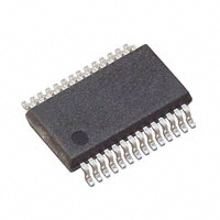
Package: 28-Pin SSOP
APPLICATIONS
•
•
•
•
USB
USB
USB
USB
Audio Speaker
Headset
Monitor
Audio Interface Box
DESCRIPTION
The PCM2900/2902 is Texas Instruments' single-chip
USB stereo audio codec with USB-compliant
full-speed protocol controller and S/PDIF (only
PCM2902). The USB protocol controller works with
no software code, but the USB descriptors can be
modified in some areas (e.g., vendor ID/product ID).
The PCM2900/2902 employs SpAct™ architecture,
TI's unique system that recovers the audio clock from
USB packet data. On-chip analog PLLs with SpAct
architecture enable playback and record with low
clock jitter and with independent playback and record
sampling rates.
The descriptor can be modified by changing a mask.
1
2
3
4
Please be aware that an important notice concerning availability, standard warranty, and use in critical applications of
Texas Instruments semiconductor products and disclaimers thereto appears at the end of this data sheet.
SpAct is a trademark of Texas Instruments.
System Two, Audio Precision are trademarks of Audio Precision, Inc.
All other trademarks are the property of their respective owners.
PRODUCTION DATA information is current as of publication date.
Products conform to specifications per the terms of the Texas
Instruments standard warranty. Production processing does not
necessarily include testing of all parameters.
Copyright © 2007–2008, Texas Instruments Incorporated
�Not Recommended for New Designs
PCM2900
PCM2902
www.ti.com
SLES035E – MARCH 2007 – REVISED MARCH 2008
This integrated circuit can be damaged by ESD. Texas Instruments recommends that all integrated circuits be handled with
appropriate precautions. Failure to observe proper handling and installation procedures can cause damage.
ESD damage can range from subtle performance degradation to complete device failure. Precision integrated circuits may be more
susceptible to damage because very small parametric changes could cause the device not to meet its published specifications.
PACKAGING ORDERING INFORMATION
PCM2900
PRODUCT
PACKAGE-LEAD
PACKAGE
DESIGNATOR
SPECIFIED
TEMPERATURE
RANGE
PCM2900E
SSOP-28
28DB
–25°C to 85°C
(1)
PACKAGE
MARKING
PCM2900E
ORDERING
NUMBER (1)
TRANSPORT
MEDIA
PCM2900E
Rails
PCM2900E/2K
Tape and reel
Models with a slash (/) are available only in tape and reel in the quantities indicated (e.g., /2K indicates 2000 devices per reel). Ordering
2000 pieces of PCM2900E/2K gets a single 2000-piece tape and reel.
PCM2902
PRODUCT
PACKAGE-LEAD
PACKAGE
DESIGNATOR
SPECIFIED
TEMPERATURE
RANGE
PACKAGE
MARKING
PCM2902E
SSOP-28
28DB
–25°C to 85°C
PCM2902E
(1)
ORDERING
NUMBER (1)
TRANSPORT
MEDIA
PCM2902E
Rails
PCM2902E/2K
Tape and reel
Models with a slash (/) are available only in tape and reel in the quantities indicated (e.g., /2K indicates 2000 devices per reel). Ordering
2000 pieces of PCM2902E/2K gets a single 2000-piece tape and reel.
ABSOLUTE MAXIMUM RATINGS
over operating free-air temperature range (unless otherwise noted) (1)
VBUS
PCM2900/PCM2902
UNIT
–0.3 to 6.5
V
Ground voltage differences, AGNDC, AGNDP, AGNDX, DGND, DGNDU
±0.1
V
SEL0, SEL1, TEST0 (DIN) (2)
–0.3 to 6.5
V
D+, D–, HID0, HID1, HID2, XTI, XTO, TEST1 (DOUT) (2), SSPND
–0.3 to (VDDI + 0.3) < 4
V
VINL, VINR, VCOM, VOUTR, VOUTL
–0.3 to (VCCCI + 0.3) < 4
V
VCCCI, VCCP1I, VCCP2I, VCCXI, VDDI
–0.3 to 4
V
±10
mA
Supply voltage
Digital input voltage
Analog input
voltage
Input current (any pins except supplies)
Ambient temperature under bias
–40 to 125
°C
Tstg
Storage temperature
–55 to 150
°C
TJ
Junction temperature
150
°C
Lead temperature (soldering)
260
°C, 5 s
Package temperature (IR reflow, peak)
250
°C
(1)
(2)
2
Stresses beyond those listed under absolute maximum ratings may cause permanent damage to the device. These are stress ratings
only, and functional operation of the device at these or any other conditions beyond those indicated under recommended operating
conditions is not implied. Exposure to absolute-maximum-rated conditions for extended periods may affect device reliability.
( ): PCM2902
Submit Documentation Feedback
Copyright © 2007–2008, Texas Instruments Incorporated
Product Folder Link(s): PCM2900 PCM2902
�Not Recommended for New Designs
PCM2900
PCM2902
www.ti.com
SLES035E – MARCH 2007 – REVISED MARCH 2008
ELECTRICAL CHARACTERISTICS
all specifications at TA = 25°C, VBUS = 5 V, fS = 44.1 kHz, fIN = 1 kHz, 16-bit data, unless otherwise noted
PARAMETER
TEST CONDITIONS
PCM2900E, PCM2902E
MIN
TYP
MAX
UNIT
DIGITAL INPUT/OUTPUT
Host interface
Apply USB Revision 1.1, full speed
Audio data format
USB isochronous data format
INPUT LOGIC
D+, D–
VIH
High-level input
voltage
XTI, HID0, HID1, and
HID2
SEL0, SEL1
DIN, PCM2902
VIL
IIH
Low-level input
voltage
High-level input
voltage
2
3.3
2.52
3.3
2
5.25
2.52
5.25
D+, D–
0.8
XTI, HID0, HID1, and
HID2
0.9
SEL0, SEL1
0.8
DIN, PCM2902
0.9
D+, D–, XTI, SEL0,
SEL1
HID0, HID1, and HID2
IIL
50
80
65
100
D+, D–, XTI, SEL0,
SEL1
HID0, HID1, and HID2
VDC
±10
VIN = 3.3 V
DIN, PCM2902
Low-level input
voltage
VDC
µA
±10
VIN = 0 V
±10
DIN, PCM2902
µA
±10
OUTPUT LOGIC
D+, D–
VOH
High-level output
voltage
2.8
DOUT, PCM2902
IOH = –4 mA
2.8
SSPND
IOH = –2 mA
2.8
VDC
D+, D–
VOL
Low-level output
voltage
0.3
DOUT, PCM2902
IOL = 4 mA
0.5
SSPND
IOL = 2 mA
0.5
VDC
CLOCK FREQUENCY
Input clock frequency, XTI
11.994
12
12.008
MHz
ADC CHARACTERISTICS
Resolution
Audio data channel
Copyright © 2007–2008, Texas Instruments Incorporated
Product Folder Link(s): PCM2900 PCM2902
8, 16
bits
1, 2
channel
Submit Documentation Feedback
3
�Not Recommended for New Designs
PCM2900
PCM2902
www.ti.com
SLES035E – MARCH 2007 – REVISED MARCH 2008
ELECTRICAL CHARACTERISTICS
all specifications at TA = 25°C, VBUS = 5 V, fS = 44.1 kHz, fIN = 1 kHz, 16-bit data, unless otherwise noted
PARAMETER
PCM2900E, PCM2902E
TEST CONDITIONS
MIN
TYP
MAX
UNIT
CLOCK FREQUENCY
fS
8, 11.025, 16, 22.05, 32, 44.1,
48
Sampling frequency
kHz
DC ACCURACY
Gain mismatch, channel-to-channel
±1
±5
% of
FSR
Gain error
±2
±10
% of
FSR
Bipolar zero error
±0
% of
FSR
DYNAMIC PERFORMANCE (1)
VCCCI = 3.67 V, VIN = –0.5 dB (2)
THD+N
Total harmonic distortion plus noise
0.01%
VIN = –0.5 dB (3)
VIN = –60 dB
SNR
0.02%
0.1%
5%
Dynamic range
A-weighted
81
89
dB
Signal-to-noise ratio
A-weighted
81
89
dB
80
85
dB
Input voltage
0.6 VCCCI
Vp-p
Center voltage
0.5 VCCCI
Channel separation
ANALOG INPUT
Input impedance
Antialiasing filter frequency response
–3 dB
fIN = 20 kHz
V
30
kΩ
150
kHz
–0.08
dB
DIGITAL FILTER PERFORMANCE
Pass band
Stop band
Stop-band attenuation
±0.05
dB
Hz
65
Delay time
LCF frequency response
Hz
0.583 fS
Pass-band ripple
td
0.454 fS
–3 dB
dB
17.4/fS
s
0.078 fS
MHz
8, 16
bits
1, 2
channel
DAC CHARACTERISTICS
Resolution
Audio data channel
CLOCK FREQUENCY
fS
(1)
(2)
(3)
4
Sampling frequency
32, 44.1, 48
kHz
fIN = 1 kHz, using a System Two™ audio measurement system by Audio Precision™ in the RMS mode with 20-kHz LPF, 400-Hz HPF in
calculation.
Using external voltage regulator for VCCCI (as shown in Figure 36 and Figure 37, using with REG103xA-A)
Using internal voltage regulator for VCCCI (as shown in Figure 38 and Figure 39)
Submit Documentation Feedback
Copyright © 2007–2008, Texas Instruments Incorporated
Product Folder Link(s): PCM2900 PCM2902
�Not Recommended for New Designs
PCM2900
PCM2902
www.ti.com
SLES035E – MARCH 2007 – REVISED MARCH 2008
ELECTRICAL CHARACTERISTICS
all specifications at TA = 25°C, VBUS = 5 V, fS = 44.1 kHz, fIN = 1 kHz, 16-bit data, unless otherwise noted
PARAMETER
TEST CONDITIONS
PCM2900E, PCM2902E
MIN
UNIT
TYP
MAX
Gain mismatch channel-to-channel
±1
±5
% of
FSR
Gain error
±2
±10
% of
FSR
Bipolar zero error
±2
DC ACCURACY
% of
FSR
DYNAMIC PERFORMANCE (1)
THD+N
SNR
VOUT = 0 dB
Total harmonic distortion plus noise
0.005%
VOUT = –60 dB
0.016%
3%
Dynamic range
EIAJ, A-weighted
87
93
Signal-to-noise ratio
EIAJ, A-weighted
90
96
dB
86
92
dB
0.6 VCCCI
Vp-p
Channel separation
dB
ANALOG OUTPUT
VO
Output voltage
Center voltage
0.5 VCCCI
Load impedance
AC coupling
–3 dB
LPF frequency response
V
10
f = 20 kHz
kΩ
250
kHz
–0.03
dB
Digital filter performance
Pass band
Stop band
Hz
±0.1
dB
0.555 fS
Hz
Pass-band ripple
Stop-band attenuation
td
0.445 fS
–43
Delay time
dB
14.3 fS
s
POWER SUPPLY REQUIREMENTS
VBUS
Voltage range
4.35
ADC, DAC operation
Supply current
PD
Suspend mode
Power dissipation
Internal power supply
voltage
(2)
5
5.25
VDC
56
67
mA
280
Suspend mode (2)
1.05
VCCCI, VCCP1I, VCCP2I,
VCCXI, and VDDI
µA
210
ADC, DAC operation
3.25
3.35
352
mW
3.5
VDC
85
°C
TEMPERATURE RANGE
Operation temperature
θJA
(1)
(2)
–25
Thermal resistance
100
°C/W
fOUT = 1 kHz, using a System Two audio measurement system by Audio Precision in the RMS mode with 20-kHz LPF, 400-Hz HPF.
Under USB suspend state
Copyright © 2007–2008, Texas Instruments Incorporated
Product Folder Link(s): PCM2900 PCM2902
Submit Documentation Feedback
5
�Not Recommended for New Designs
PCM2900
PCM2902
www.ti.com
SLES035E – MARCH 2007 – REVISED MARCH 2008
PIN ASSIGNMENTS
PCM2900
(Top View)
D+
D–
VBUS
DGNDU
HID0
HID1
HID2
SEL0
SEL1
VCCCI
AGNDC
VINL
VINR
VCOM
1
2
3
4
5
6
7
8
9
10
11
12
13
14
PCM2902
(Top View)
28
27
26
25
24
23
22
21
20
19
18
17
16
15
SSPND
VDDI
DGND
TEST1
TEST0
VCCXI
D+
D–
1
2
3
4
5
6
7
8
9
10
11
12
13
14
VBUS
AGNDX
XTI
XTO
VCCP2I
DGNDU
HID0
HID1
HID2
SEL0
SEL1
VCCCI
AGNDP
VCCP1I
VOUTL
VOUTR
AGNDC
VINL
VINR
VCOM
28
27
26
25
24
23
22
21
20
19
18
17
16
15
SSPND
VDDI
DGND
DOUT
DIN
VCCXI
AGNDX
XTI
XTO
VCCP2I
AGNDP
VCCP1I
VOUTL
VOUTR
P0007-06
6
Submit Documentation Feedback
Copyright © 2007–2008, Texas Instruments Incorporated
Product Folder Link(s): PCM2900 PCM2902
�Not Recommended for New Designs
PCM2900
PCM2902
www.ti.com
SLES035E – MARCH 2007 – REVISED MARCH 2008
PCM2900 TERMINAL FUNCTIONS
TERMINAL
NAME
NO.
I/O
DESCRIPTION
AGNDC
11
–
Analog ground for codec
AGNDP
18
–
Analog ground for PLL
AGNDX
22
–
Analog ground for oscillator
D–
2
I/O
USB differential input/output minus (1)
D+
1
I/O
USB differential input/output plus (1)
DGND
26
–
DGNDU
4
–
Digital ground for USB transceiver
HID0
5
I
HID key state input (mute), active-high (2)
HID1
6
I
HID key state input (volume up), active-high (2)
HID2
7
I
HID key state input (volume down), active-high (2)
SEL0
8
I
Must be set to high (3)
SEL1
9
I
Must be set to high (3)
SSPND
28
O
Suspend flag, active-low (Low: suspend, High: operational)
TEST0
24
I
Test pin, must be connected to GND
TEST1
25
O
Test pin, must be left open
VBUS
3
–
Connect to USB power (VBUS)
VCCCI
10
–
Internal analog power supply for codec (4)
VCCP1I
17
–
Internal analog power supply for PLL (4)
VCCP2I
19
–
Internal analog power supply for PLL (4)
VCCXI
23
–
Internal analog power supply for oscillator (4)
VCOM
14
–
Common for ADC/DAC (VCCCI/2) (4)
VDDI
27
–
Internal digital power supply (4)
VINL
12
I
ADC analog input for L-channel
VINR
13
I
ADC analog input for R-channel
VOUTL
16
O
DAC analog output for L-channel
VOUTR
15
O
DAC analog output for R-channel
XTI
21
I
Crystal oscillator input
XTO
20
O
Crystal oscillator output
(1)
(2)
(3)
(4)
(5)
Digital ground
(5)
LV-TTL level
3.3-V CMOS-level input with internal pulldown. This pin informs the PC of serviceable control signals such as mute, volume up, or
volume down, which have no connection with the internal DAC or ADC directly. See the Interface #3 and End-Points sections.
TTL Schmitt trigger, 5-V tolerant
Connect a decoupling capacitor to GND.
3.3-V CMOS-level input
Copyright © 2007–2008, Texas Instruments Incorporated
Product Folder Link(s): PCM2900 PCM2902
Submit Documentation Feedback
7
�Not Recommended for New Designs
PCM2900
PCM2902
www.ti.com
SLES035E – MARCH 2007 – REVISED MARCH 2008
PCM2902 TERMINAL FUNCTIONS
TERMINAL
NAME
NO.
I/O
DESCRIPTION
AGNDC
11
–
Analog ground for codec
AGNDP
18
–
Analog ground for PLL
AGNDX
22
–
Analog ground for oscillator
D–
2
I/O
USB differential input/output minus (1)
D+
1
I/O
USB differential input/output plus (1)
DGND
26
–
DGNDU
4
–
Digital ground for USB transceiver
DIN
24
I
S/PDIF input (2)
DOUT
25
O
S/PDIF output
HID0
5
I
HID key state input (mute), active high (3)
HID1
6
I
HID key state input (volume up), active high (3)
HID2
7
I
HID key state input (volume down), active high (3)
SEL0
8
I
Must be set to high (4)
SEL1
9
I
Must be set to high (4)
SSPND
28
O
Suspend flag, active-low (Low: suspend, High: operational)
VBUS
3
–
Connect to USB power (VBUS)
VCCCI
10
–
Internal analog power supply for codec (5)
VCCP1I
17
–
Internal analog power supply for PLL (5)
VCCP2I
19
–
Internal analog power supply for PLL (5)
VCCXI
23
–
Internal analog power supply for oscillator (5)
VCOM
14
–
Common for ADC/DAC (VCCCI/2) (5)
VDDI
27
–
Internal digital power supply
VINL
12
I
ADC analog input for L-channel
VINR
13
I
ADC analog input for R-channel
VOUTL
16
O
DAC analog output for L-channel
VOUTR
15
O
DAC analog output for R-channel
XTI
21
I
Crystal oscillator input (6)
XTO
20
O
Crystal oscillator output
(1)
(2)
(3)
(4)
(5)
(6)
8
Digital ground
LV-TTL level
3.3-V CMOS-level input with internal pulldown, 5-V tolerant
3.3-V CMOS-level input with internal pulldown. This pin informs the PC of serviceable control signals such as mute, volume up, or
volume down, which have no connection with the internal DAC or ADC directly. See the Interface #3 and End-Points sections.
TTL Schmitt trigger, 5-V tolerant
Connect a decoupling capacitor to GND.
3.3-V CMOS-level input
Submit Documentation Feedback
Copyright © 2007–2008, Texas Instruments Incorporated
Product Folder Link(s): PCM2900 PCM2902
�Not Recommended for New Designs
PCM2900
PCM2902
www.ti.com
SLES035E – MARCH 2007 – REVISED MARCH 2008
PCM2900 FUNCTIONAL BLOCK DIAGRAM
VCCCI
VCCP1I
VCCP2I
VCCXI
VDDI
AGNDC
AGNDP
AGNDX
DGND
DGNDU
5-V to 3.3-V Voltage Regulator
Power
Manager
TEST0
SSPND
TEST1
VBUS
VINL
ISO-In
End-Point
USB SIE
VINR
Analog
PLL
VCOM
Selector
Analog
PLL
XCVR
FIFO
ADC
D+
D–
Control
End-Point
SEL0
SEL1
VOUTL
FIFO
DAC
ISO-Out
End-Point
VOUTR
HID0
HID1
HID2
HID
End-Point
USB
Protocol
Controller
96 MHz
PLL (´8)
XTI
12 MHz
Tracker
(SpAct)
XTO
B0238-01
Copyright © 2007–2008, Texas Instruments Incorporated
Product Folder Link(s): PCM2900 PCM2902
Submit Documentation Feedback
9
�Not Recommended for New Designs
PCM2900
PCM2902
www.ti.com
SLES035E – MARCH 2007 – REVISED MARCH 2008
PCM2902 FUNCTIONAL BLOCK DIAGRAM
VCCCI
VCCP1I
VCCP2I
VCCXI
VDDI
AGNDC
AGNDP
AGNDX
DGND
DGNDU
5-V to 3.3-V Voltage Regulator
Lock
DIN
Power
Manager
SSPND
S/PDIF Decoder
VBUS
VINL
ISO-In
End-Point
USB SIE
VINR
Analog
PLL
VCOM
Selector
Analog
PLL
XCVR
FIFO
ADC
D+
D–
Control
End-Point
SEL0
SEL1
VOUTL
FIFO
DAC
ISO-Out
End-Point
VOUTR
DOUT
HID
End-Point
S/PDIF Encoder
HID0
HID1
HID2
USB
Protocol
Controller
96 MHz
PLL (´8)
XTI
12 MHz
Tracker
(SpAct)
XTO
B0239-01
10
Submit Documentation Feedback
Copyright © 2007–2008, Texas Instruments Incorporated
Product Folder Link(s): PCM2900 PCM2902
�Not Recommended for New Designs
PCM2900
PCM2902
www.ti.com
SLES035E – MARCH 2007 – REVISED MARCH 2008
PCM2900/2902 DIAGRAM OF ANALOG FRONT-END (RIGHT CHANNEL)
4.7 mF
+
VINR
30 kW
–
13
–
(+)
+
+
(–)
Delta-Sigma
Modulator
VCOM
14
+
(VCCCI/2)
10 mF
Reference
S0011-06
Copyright © 2007–2008, Texas Instruments Incorporated
Product Folder Link(s): PCM2900 PCM2902
Submit Documentation Feedback
11
�Not Recommended for New Designs
PCM2900
PCM2902
www.ti.com
SLES035E – MARCH 2007 – REVISED MARCH 2008
TYPICAL CHARACTERISTICS
All specifications at TA = 25°C, VBUS = 5 V, fS = 44.1 kHz, fin = 1 kHz, 16-bit data, using REG 103xA-A, unless otherwise noted
ADC
TOTAL HARMONIC DISTORTION + NOISE at –0.5 dB
vs
FREE-AIR TEMPERATURE
DYNAMIC RANGE and SNR
vs
FREE-AIR TEMPERATURE
95
0.009
Dynamic Range and SNR − dB
THD+N − Total Harmonic Distortion + Noise − %
0.010
0.008
0.007
0.006
0.005
SNR
85
80
0.004
0.003
−50
−25
0
25
50
75
TA − Free-Air Temperature − °C
75
−50
100
−25
25
50
G001
Figure 1.
Figure 2.
TOTAL HARMONIC DISTORTION + NOISE at –0.5 dB
vs
SUPPLY VOLTAGE
DYNAMIC RANGE and SNR
vs
SUPPLY VOLTAGE
75
100
G002
95
Dynamic Range and SNR − dB
0.009
0.008
0.007
0.006
0.005
Dynamic Range
90
SNR
85
80
0.004
0.003
4.0
4.5
5.0
5.5
VBUS − Supply Voltage − V
75
4.0
4.5
Submit Documentation Feedback
5.0
VBUS − Supply Voltage − V
G003
Figure 3.
12
0
TA − Free-Air Temperature − °C
0.010
THD+N − Total Harmonic Distortion + Noise − %
Dynamic Range
90
5.5
G004
Figure 4.
Copyright © 2007–2008, Texas Instruments Incorporated
Product Folder Link(s): PCM2900 PCM2902
�Not Recommended for New Designs
PCM2900
PCM2902
www.ti.com
SLES035E – MARCH 2007 – REVISED MARCH 2008
TYPICAL CHARACTERISTICS (continued)
All specifications at TA = 25°C, VBUS = 5 V, fS = 44.1 kHz, fin = 1 kHz, 16-bit data, using REG 103xA-A, unless otherwise noted
TOTAL HARMONIC DISTORTION + NOISE at –0.5 dB
vs
SAMPLING FREQUENCY
DYNAMIC RANGE AND SNR
vs
SAMPLING FREQUENCY
95
0.09
0.009
Dynamic Range and SNR − dB
THD+N − Total Harmonic Distortion + Noise − %
0.10
0.010
0.08
0.008
0.07
0.007
0.06
0.006
0.05
0.005
Dynamic Range
90
SNR
85
80
0.04
0.004
75
0.03
0.003
35
30
40
45
30
50
35
40
45
50
fS − Sampling Frequency − kHz
fS − Sampling Frequency − kHz
G006
G005
Figure 5.
Figure 6.
TOTAL HARMONIC DISTORTION + NOISE at 0 dB
vs
FREE-AIR TEMPERATURE
DYNAMIC RANGE AND SNR
vs
FREE-AIR TEMPERATURE
DAC
98
97
0.007
Dynamic Range and SNR − dB
THD+N − Total Harmonic Distortion + Noise − %
0.008
0.006
0.005
0.004
SNR
96
95
Dynamic Range
94
93
92
91
0.003
−50
−25
0
25
50
75
TA − Free-Air Temperature − °C
100
90
−50
−25
0
25
50
75
TA − Free-Air Temperature − °C
G007
Figure 7.
100
G008
Figure 8.
Copyright © 2007–2008, Texas Instruments Incorporated
Product Folder Link(s): PCM2900 PCM2902
Submit Documentation Feedback
13
�Not Recommended for New Designs
PCM2900
PCM2902
www.ti.com
SLES035E – MARCH 2007 – REVISED MARCH 2008
TYPICAL CHARACTERISTICS (continued)
All specifications at TA = 25°C, VBUS = 5 V, fS = 44.1 kHz, fin = 1 kHz, 16-bit data, using REG 103xA-A, unless otherwise noted
TOTAL HARMONIC DISTORTION + NOISE at 0 dB
vs
SUPPLY VOLTAGE
DYNAMIC RANGE AND SNR
vs
SUPPLY VOLTAGE
98
97
0.007
Dynamic Range and SNR − dB
THD+N − Total Harmonic Distortion + Noise − %
0.008
0.006
0.005
0.004
95
Dynamic Range
94
93
92
91
0.003
4.0
4.5
5.0
90
4.0
5.5
VBUS − Supply Voltage − V
4.5
5.5
G009
Figure 9.
Figure 10.
TOTAL HARMONIC DISTORTION + NOISE at 0 dB
vs
SAMPLING FREQUENCY
DYNAMIC RANGE AND SNR
vs
SAMPLING FREQUENCY
G010
98
97
SNR
Dynamic Range and SNR − dB
0.007
0.006
0.005
0.004
96
95
94
Dynamic Range
93
92
91
90
0.003
30
35
40
45
fS − Sampling Frequency − kHz
30
50
35
Submit Documentation Feedback
40
45
fS − Sampling Frequency − kHz
G011
Figure 11.
14
5.0
VBUS − Supply Voltage − V
0.008
THD+N − Total Harmonic Distortion + Noise − %
SNR
96
50
G012
Figure 12.
Copyright © 2007–2008, Texas Instruments Incorporated
Product Folder Link(s): PCM2900 PCM2902
�Not Recommended for New Designs
PCM2900
PCM2902
www.ti.com
SLES035E – MARCH 2007 – REVISED MARCH 2008
TYPICAL CHARACTERISTICS (continued)
All specifications at TA = 25°C, VBUS = 5 V, fS = 44.1 kHz, fin = 1 kHz, 16-bit data, using REG 103xA-A, unless otherwise noted
SUPPLY CURRENT
60
0.28
Operational
50
0.26
Suspend
40
0.24
0.22
30
20
4.00
4.25
4.50
4.75
5.00
5.25
ICC − Suspend Supply Current − mA
ICC − Operational Supply Current − mA
OPERATIONAL AND SUSPEND SUPPLY CURRENT
vs
SUPPLY VOLTAGE
70
0.30
0.20
5.50
VBUS − Supply Voltage − V
G013
Figure 13.
OPERATIONAL SUPPLY CURRENT
vs
SAMPLING FREQUENCY
SUSPEND SUPPLY CURRENT
vs
FREE-AIR TEMPERATURE
0.40
ICC − Suspend Supply Current − mA
ICC − Operational Supply Current − mA
70
60
50
ADC and DAC
40
30
20
30
35
40
45
fS − Sampling Frequency − kHz
50
0.35
0.30
USB Spec Limit for Device (0.3 mA)
0.25
0.20
0.15
0.10
−40
−20
G014
Figure 14.
0
20
40
60
80
TA − Free-Air Temperature − °C
100
G015
Figure 15.
Copyright © 2007–2008, Texas Instruments Incorporated
Product Folder Link(s): PCM2900 PCM2902
Submit Documentation Feedback
15
�Not Recommended for New Designs
PCM2900
PCM2902
www.ti.com
SLES035E – MARCH 2007 – REVISED MARCH 2008
TYPICAL CHARACTERISTICS (continued)
All specifications at TA = 25°C, VBUS = 5 V, fS = 44.1 kHz, fin = 1 kHz, 16-bit data, unless otherwise noted
ADC DIGITAL DECIMATION FILTER FREQUENCY RESPONSE
OVERALL CHARACTERISTICS
STOP-BAND ATTENUATION
0
0
−10
−20
−20
−40
Amplitude − dB
Amplitude − dB
−30
−60
−80
−100
−40
−50
−60
−70
−120
−80
−140
−90
−100
0.0
−160
0
8
16
24
Frequency [y fS]
32
0.2
G016
Figure 16.
0.8
1.0
G017
TRANSITION-BAND RESPONSE
0
0.0
−4
Amplitude − dB
Amplitude − dB
PASS-BAND RIPPLE
−0.2
−0.4
−8
−12
−16
−0.6
0.1
0.2
0.3
Frequency [y fS]
0.4
0.5
−20
0.46
0.48
Submit Documentation Feedback
0.50
Frequency [y fS]
G018
Figure 18.
16
0.6
Figure 17.
0.2
−0.8
0.0
0.4
Frequency [y fS]
0.52
0.54
G019
Figure 19.
Copyright © 2007–2008, Texas Instruments Incorporated
Product Folder Link(s): PCM2900 PCM2902
�Not Recommended for New Designs
PCM2900
PCM2902
www.ti.com
SLES035E – MARCH 2007 – REVISED MARCH 2008
TYPICAL CHARACTERISTICS (continued)
All specifications at TA = 25°C, VBUS = 5 V, fS = 44.1 kHz, fin = 1 kHz, 16-bit data, unless otherwise noted
ADC DIGITAL HIGH-PASS FILTER FREQUENCY RESPONSE
STOP-BAND CHARACTERISTICS
PASS-BAND CHARACTERISTICS
0.0
0
−10
−0.2
−20
Amplitude − dB
Amplitude − dB
−30
−40
−50
−60
−0.4
−0.6
−70
−0.8
−80
−90
−100
0.0
−1.0
0.1
0.2
0.3
Frequency [y fS/1000]
0
0.4
1
2
3
Frequency [y fS/1000]
G020
Figure 20.
4
G021
Figure 21.
ADC ANALOG ANTIALIASING FILTER FREQUENCY RESPONSE
PASS-BAND CHARACTERISTICS
0.0
−10
−0.2
Amplitude − dB
Amplitude − dB
STOP-BAND CHARACTERISTICS
0
−20
−30
−0.4
−0.6
−0.8
−40
−50
1
10
100
1k
10k
−1.0
0.01
0.1
1
10
100
f − Frequency − kHz
f − Frequency − kHz
G023
G022
Figure 22.
Figure 23.
Copyright © 2007–2008, Texas Instruments Incorporated
Product Folder Link(s): PCM2900 PCM2902
Submit Documentation Feedback
17
�Not Recommended for New Designs
PCM2900
PCM2902
www.ti.com
SLES035E – MARCH 2007 – REVISED MARCH 2008
TYPICAL CHARACTERISTICS (continued)
All specifications at TA = 25°C, VBUS = 5 V, fS = 44.1 kHz, fin = 1 kHz, 16-bit data, unless otherwise noted
DAC DIGITAL INTERPOLATION FILTER FREQUENCY RESPONSE
STOP-BAND ATTENUATION
PASS-BAND RIPPLE
0
0.2
−10
−20
0.0
Amplitude − dB
Amplitude − dB
−30
−40
−50
−60
−0.2
−0.4
−70
−80
−0.6
−90
−100
0
1
2
3
−0.8
0.0
4
Frequency [y fS]
0.1
0.2
0.3
Frequency [y fS]
G024
Figure 24.
0.4
0.5
G025
Figure 25.
TRANSITION-BAND RESPONSE
0
−2
−4
Amplitude − dB
−6
−8
−10
−12
−14
−16
−18
−20
0.46 0.47 0.48
0.49 0.50 0.51
0.52 0.53 0.54
Frequency [y fS]
G026
Figure 26.
18
Submit Documentation Feedback
Copyright © 2007–2008, Texas Instruments Incorporated
Product Folder Link(s): PCM2900 PCM2902
�Not Recommended for New Designs
PCM2900
PCM2902
www.ti.com
SLES035E – MARCH 2007 – REVISED MARCH 2008
TYPICAL CHARACTERISTICS (continued)
All specifications at TA = 25°C, VBUS = 5 V, fS = 44.1 kHz, fin = 1 kHz, 16-bit data, unless otherwise noted
DAC ANALOG FIR FILTER FREQUENCY RESPONSE
PASS-BAND CHARACTERISTICS
0.2
−10
0.0
Amplitude − dB
Amplitude − dB
STOP-BAND CHARACTERISTICS
0
−20
−30
−0.2
−0.4
−0.6
−40
−0.8
0.0
−50
0
8
16
24
Frequency [y fS]
32
0.1
0.2
0.3
0.4
Frequency [y fS]
G027
Figure 27.
0.5
G028
Figure 28.
DAC ANALOG LOW-PASS FILTER FREQUENCY RESPONSE
PASS-BAND CHARACTERISTICS
0.0
−10
−0.2
Amplitude − dB
Amplitude − dB
STOP-BAND CHARACTERISTICS
0
−20
−30
−0.4
−0.6
−0.8
−40
−50
1
10
100
1k
10k
−1.0
0.01
0.1
1
10
100
f − Frequency − kHz
f − Frequency − kHz
G030
G029
Figure 29.
Figure 30.
Copyright © 2007–2008, Texas Instruments Incorporated
Product Folder Link(s): PCM2900 PCM2902
Submit Documentation Feedback
19
�Not Recommended for New Designs
PCM2900
PCM2902
www.ti.com
SLES035E – MARCH 2007 – REVISED MARCH 2008
USB INTERFACE
Control data and audio data are transferred to the PCM2900/2902 via D+ (pin 1) and D– (pin 2). All data to/from
the PCM2900/2902 is transferred at full speed. The device descriptor contains the information described in
Table 1. The device descriptor can be modified on request; contact a Texas Instruments representative for
details.
Table 1. Device Description
USB revision
1.1 compliant
Device class
0x00 (device-defined interface level)
Device subclass
0x00 (not specified)
Device protocol
0x00 (not specified)
Max packet size for end-point 0
8 bytes
Vendor ID
0x08BB (default value, can be modified)
Product ID
0x2900 / 0x2902 (default value, can be modified)
Device release number
1.0 (0x0100)
Number of configurations
1
Vendor strings
String #1 (see Table 3)
Product strings
String #2 (see Table 3)
Serial number
Not supported
The configuration descriptor contains the information described in Table 2. The configuration descriptor can be
modified on request; contact a Texas Instruments representative for details.
Table 2. Configuration Descriptor
Interface
Four interfaces
Power attribute
0x80 (Bus powered, no remote
wakeup)
Max power
0x32 (100 mA. Default value, can be
modified)
The string descriptor contains the information described in Table 3. The string descriptor can be modified on
request; contact a Texas Instruments representative for details.
Table 3. String Descriptor
#0
0x0409
#1
Burr-Brown from TI (default value, can be modified)
#2
USB audio codec (default value, can be modified)
A
DEVICE CONFIGURATION
Figure 31 illustrates the USB audio function topology. The PCM2900/2902 has four interfaces. Each interface is
constructed by alternative settings.
20
Submit Documentation Feedback
Copyright © 2007–2008, Texas Instruments Incorporated
Product Folder Link(s): PCM2900 PCM2902
�Not Recommended for New Designs
PCM2900
PCM2902
www.ti.com
SLES035E – MARCH 2007 – REVISED MARCH 2008
End-Point #0
Default End-Point
FU
Analog Out
End-Point #2
(IF #1)
IT
TID1
OT
TID2
Audio Streaming Interface
UID3
Analog In
End-Point #4
(IF #2)
IT
TID4
OT
TID5
Audio Streaming Interface
Standard Audio Control Interface (IF #0)
End-Point #5
(IF #3)
HID Interface
PCM2900/2902
M0024-03
Figure 31. USB Audio Function Topology
Interface #0
Interface #0 is defined as the control interface. Alternative setting #0 is the only possible setting for interface #0.
Alternative setting #0 describes the standard audio control interface. A terminal constructs the audio control
interface. The PCM2900/2902 has five terminals as follows:
• Input terminal (IT #1) for isochronous-out stream
• Output terminal (OT #2) for audio analog output
• Feature unit (FU #3) for DAC digital attenuator
• Input terminal (IT #4) for audio analog input
• Output terminal (OT #5) for isochronous-in stream
Input terminal #1 is defined as USB stream (terminal type 0x0101). Input terminal #1 can accept 2-channel audio
streams constructed by left and right channels. Output terminal #2 is defined as a speaker (terminal type
0x0301). Input terminal #4 is defined as a microphone (terminal type 0x0201). Output terminal #5 is defined as a
USB stream (terminal type 0x0101). Output terminal #5 can generate 2-channel audio streams constructed by
left and right channels. Feature unit #3 supports the following sound control features.
• Volume control
• Mute control
The built-in digital volume controller can be manipulated by an audio class specific request from 0 dB to -64 dB
Copyright © 2007–2008, Texas Instruments Incorporated
Product Folder Link(s): PCM2900 PCM2902
Submit Documentation Feedback
21
�Not Recommended for New Designs
PCM2900
PCM2902
www.ti.com
SLES035E – MARCH 2007 – REVISED MARCH 2008
in 1-dB steps. Changes are made by incrementing or decrementing by one step (1 dB) for every 1/fS time interval
until the volume level has reached the requested value. Each channel can be set for different values. The master
volume control is not supported. A request to the master volume is stalled and ignored. The built-in digital mute
controller can be manipulated by audio class specific request. A master mute control request is acceptable. A
request to an individual channel is stalled and ignored.
Interface #1
Interface #1 is the audio streaming data-out interface. Interface #1 has the following seven alternative settings.
Alternative setting #0 is the zero bandwidth setting. All other alternative settings are operational settings.
ALTERNATIVE
SETTING
DATA FORMAT
00
TRANSFER
MODE
SAMPLING RATE
(kHz)
Zero Bandwidth
01
16 bit
Stereo
2s complement (PCM)
Adaptive
32, 44.1, 48
02
16 bit
Mono
2s complement (PCM)
Adaptive
32, 44.1, 48
03
8 bit
Stereo
2s complement (PCM)
Adaptive
32, 44.1, 48
04
8 bit
Mono
2s complement (PCM)
Adaptive
32, 44.1, 48
05
8 bit
Stereo
Offset binary (PCM8)
Adaptive
32, 44.1, 48
06
8 bit
Mono
Offset binary (PCM8)
Adaptive
32, 44.1, 48
Interface #2
Interface #2 is the audio streaming data-in the interface. Interface #2 has the following 19 alternative settings.
Alternative setting #0 is the zero bandwidth setting. All other alternative settings are operational settings.
ALTERNATIVE
SETTING
DATA FORMAT
00
TRANSFER
MODE
SAMPLING RATE
(kHz)
48
Zero Bandwidth
01
16 bit
Stereo
2s complement (PCM)
Asynchronous
02
16 bit
Mono
2s complement (PCM)
Asynchronous
48
03
16 bit
Stereo
2s complement (PCM)
Asynchronous
44.1
04
16 bit
Mono
2s complement (PCM)
Asynchronous
44.1
05
16 bit
Stereo
2s complement (PCM)
Asynchronous
32
06
16 bit
Mono
2s complement (PCM)
Asynchronous
32
07
16 bit
Stereo
2s complement (PCM)
Asynchronous
22.05
08
16 bit
Mono
2s complement (PCM)
Asynchronous
22.05
09
16 bit
Stereo
2s complement (PCM)
Asynchronous
16
0A
16 bit
Mono
2s complement (PCM)
Asynchronous
16
0B
8 bit
Stereo
2s complement (PCM)
Asynchronous
16
0C
8 bit
Mono
2s complement (PCM)
Asynchronous
16
0D
8 bit
Stereo
2s complement (PCM)
Asynchronous
8
0E
8 bit
Mono
2s complement (PCM)
Asynchronous
8
0F
16 bit
Stereo
2s complement (PCM)
Synchronous
11.025
10
16 bit
Mono
2s complement (PCM)
Synchronous
11.025
11
8 bit
Stereo
2s complement (PCM)
Synchronous
11.025
12
8 bit
Mono
2s complement (PCM)
Synchronous
11.025
Interface #3
Interface #3 is the interrupt data-in interface. Alternative setting #0 is the only possible setting for interface #3.
Interface #3 constructs the HID consumer control device and reports the following three key statuses.
• Mute (0xE209)
• Volume up (0xE909)
• Volume down (0xEA09)
22
Submit Documentation Feedback
Copyright © 2007–2008, Texas Instruments Incorporated
Product Folder Link(s): PCM2900 PCM2902
�Not Recommended for New Designs
PCM2900
PCM2902
www.ti.com
SLES035E – MARCH 2007 – REVISED MARCH 2008
End-Points
The PCM2900/2902 has the following four end-points.
• Control end-point (EP #0)
• Isochronous-out audio data stream end-point (EP #2)
• Isochronous-in audio data stream end-point (EP #4)
• HID end-point (EP #5)
The control end-point is a default end-point. The control end-point is used to control all functions of the
PCM2900/2902 by the standard USB request and USB audio class specific request from the host. The
isochronous-out audio data stream end-point is an audio sink end-point, which receives the PCM audio data. The
isochronous-out audio data stream end-point accepts the adaptive transfer mode. The isochronous-in audio data
stream end-point is an audio source end-point, which transmits the PCM audio data. The isochronous-in audio
data stream end-point uses asynchronous transfer mode. The HID end-point is an interrupt-in end-point. HID
end-point reports HID0, HID1, and HID2 pin status every 32 ms.
The human interface device (HID) pins are defined as consumer control devices. The HID function is designed
as an independent end-point from both isochronous-in and -out end-points. This means that the result of
affection for the HID operation depends on the host software. Typically, the HID function is affected for the
primary audio-out device.
Clock and Reset
The PCM2900/2902 requires a 12-MHz (±500 ppm) clock for the USB and audio function, which can be
generated by a built-in crystal oscillator with a 12-MHz crystal resonator. The 12-MHz crystal resonator must be
connected to XTI (pin 21) and XTO (pin 20) with one high (1-MΩ) resistor and two small capacitors, the
capacitance of which depends on the load capacitance of the crystal resonator. The external clock can be
supplied from XTI (pin 21). If the external clock is supplied, XTO (pin 20) must be left open. Because of no
clock-disabling signal, it is not recommended to use the external clock supply. SSPND (pin 28) is unable to use
clock disabling.
The PCM2900/2902 has an internal power-on reset circuit, which works automatically when VBUS (pin 3) exceeds
2.5 V typical (2.7 V–2.2 V), and about 700 µs is required until internal reset release.
Digital Audio Interface (PCM2902)
The PCM2902 employs both S/PDIF input and output. Isochronous-out data from the host is encoded to the
S/PDIF output and the DAC analog output. Input data is selected as either S/PDIF or ADC analog input. When
the device detects an S/PDIF input and successfully locks the received data, the isochronous-in transfer data
source is automatically selected from S/PDIF itself; otherwise, the data source is selected to ADC analog input.
Supported Input Data (PCM2902)
The following data formats are accepted by the S/PDIF input and output. All other data formats are unable to use
S/PDIF.
• 48-kHz 16-bit stereo
• 44.1-kHz 16-bit stereo
• 32-kHz 16-bit stereo
Mismatch between input data format and host command may cause unexpected results except in the following
conditions.
• Record monaural format from stereo data input at the same data rate
• Record 8-bit format from 16-bit data input at the same data rate
A combination between the above conditions is not accepted.
For the playback, all possible data rate source is converted to 16-bit stereo format at the same source data rate.
Copyright © 2007–2008, Texas Instruments Incorporated
Product Folder Link(s): PCM2900 PCM2902
Submit Documentation Feedback
23
�Not Recommended for New Designs
PCM2900
PCM2902
www.ti.com
SLES035E – MARCH 2007 – REVISED MARCH 2008
Channel Status Information (PCM2902)
The channel status information is fixed as consumer application, PCM mode, copyright, and digital/digital
converter. All other bits are fixed as 0s except for the sample frequency, which is set automatically according to
the data received through the USB.
Copyright Management (PCM2902)
Isochronous-in data is affected by the serial copy management system (SCMS). Where receiving digital audio
data that is indicated as original data in the control bit, input digital audio data transfers to the host. If the data is
indicated as first generation or higher, transferred data is selected to analog input.
Digital audio data output is always encoded as original with SCMS control.
The implementation of this feature is an option for the customer. Note that it is the user's responsibility whether
they implement this feature in their product or not.
INTERFACE SEQUENCE
Power On, Attach, and Playback Sequence
The PCM2900/2902 is ready for setup when the reset sequence has finished and the USB bus is attached. After
connection has been established by setup, the PCM2900/2902 is ready to accept USB audio data. While waiting,
the audio data (idle state) and analog output are set to bipolar zero (BPZ).
When receiving the audio data, the PCM2900/2902 stores the first audio packet, which contained 1-ms audio
data, into the internal storage buffer. The PCM2900/2902 starts playing the audio data when detecting the
following start of frame (SOF) packet.
5 V (Typ)
VBUS (Pin 3)
2.5 V (Typ)
0V
Bus Reset
st
1 Audio Data
Set Configuration
2
nd
Audio Data
Bus Idle
D+/D–
SOF
SOF
SOF
SSPND
BPZ
VOUTL
VOUTR
700 ms
Device Setup
1 ms
Internal Reset
Ready for Setup
Ready for Playback
T0055-02
Figure 32. Initial Sequence
24
Submit Documentation Feedback
Copyright © 2007–2008, Texas Instruments Incorporated
Product Folder Link(s): PCM2900 PCM2902
�Not Recommended for New Designs
PCM2900
PCM2902
www.ti.com
SLES035E – MARCH 2007 – REVISED MARCH 2008
Play, Stop, and Detach Sequence
When the host finishes or aborts the playback, the PCM2900/2902 stops playing after the last audio data has
played.
Record Sequence
The PCM2900/2902 starts the audio capture into the internal memory after receiving the SET_INTERFACE
command.
Suspend and Resume Sequence
The PCM2900/2902 enters the suspend state after it sees a constant idle state on the USB bus, approximately
5 ms. While the PCM2900/2902 enters the suspend state, SSPND flag (pin 28) is asserted. The PCM2900/2902
wakes up immediately when detecting the non-idle state on the USB bus.
VBUS (Pin 3)
Audio Data
Last Audio Data
Audio Data
D+/D–
SOF
SOF
SOF
SOF
SOF
VOUTL
VOUTR
Detach
1 ms
T0056-02
Figure 33. Play, Stop, and Detach
Audio Data
SET_INTERFACE
IN Token
Audio Data
IN Token
Audio Data
IN Token
D+/D–
SOF
SOF
SOF
SOF
SOF
VINL
VINR
1 ms
T0259-01
Figure 34. Record Sequence
Copyright © 2007–2008, Texas Instruments Incorporated
Product Folder Link(s): PCM2900 PCM2902
Submit Documentation Feedback
25
�Not Recommended for New Designs
PCM2900
PCM2902
www.ti.com
SLES035E – MARCH 2007 – REVISED MARCH 2008
Idle
D+/D–
SSPND
Active
5 ms
Suspend
Active
T0057-02
Figure 35. Suspend and Resume
26
Submit Documentation Feedback
Copyright © 2007–2008, Texas Instruments Incorporated
Product Folder Link(s): PCM2900 PCM2902
�Not Recommended for New Designs
PCM2900
PCM2902
www.ti.com
SLES035E – MARCH 2007 – REVISED MARCH 2008
PCM2900 TYPICAL CIRCUIT CONNECTION 1
Figure 36 illustrates a typical circuit connection for a high-performance application. The circuit illustrated is for
information only. The whole board design should be considered to meet the USB specification as a
USB-compliant product.
1.5 kW ´ 3
1.5 kW
PCM2900
22 W
D+
22 W
D–
1 D+
SSPND
28
2
D–
VDDI
27
3
VBUS
DGND
26
4
DGNDU
TEST1
25
5
HID0
TEST0
24
6
HID1
VCCXI
23
7
HID2
AGNDX
22
8
SEL0
XTI
21
9
SEL1
XTO
20
10
VCCCI
VCCP2I
19
AGNDP
18
2.2 W
VBUS
1 mF
GND
IC1
IN OUT GND ADJ EN
5
3
4
1
2
C13
C4
D1
12 MHz
C7
11
AGNDC
12
VINL
VCCP1I
17
13
VINR
VOUTL
16
14
VCOM
VOUTR
15
C1
+
27 kW
C5
1 MW
C6
3.6 V–
3.85 V
+
C9
C10
C3
13 kW
+
C2
+
MUTE/
Power
Down
C8
+
C11
+
C12
LPF,
Amp
LPF,
Amp
S0264-03
NOTE: C1, C2: 10 µF
C3, C4, C7, C8, C13: 1 µF (These capacitors must be less than 2 µF.)
C5, C6: 10 pF to 33 pF (depending on crystal resonator)
C9, C10, C11, C12: The capacitance may vary depending on design.
IC1: REG103xA-A (TI) or equivalent. Analog performance may vary depending on IC1.
D1: Schottky barrier diode (VF ≤ 350 mV at 10 mA, IR ≤ 2 µA at 4 V)
Figure 36. Bus-Powered Configuration for High-Performance Application
Copyright © 2007–2008, Texas Instruments Incorporated
Product Folder Link(s): PCM2900 PCM2902
Submit Documentation Feedback
27
�Not Recommended for New Designs
PCM2900
PCM2902
www.ti.com
SLES035E – MARCH 2007 – REVISED MARCH 2008
PCM2902 TYPICAL CIRCUIT CONNECTION 1
Figure 37 illustrates a typical circuit connection for a high-performance application. The circuit illustrated is for
information only. The whole board design should be considered to meet the USB specification as a
USB-compliant product.
1.5 kW ´ 3
1.5 kW
PCM2902
22 W
D+
22 W
D–
1 D+
SSPND
28
2
D–
VDDI
27
3
VBUS
DGND
26
4
DGNDU
DOUT
25
5
HID0
DIN
24
6
HID1
VCCXI
23
7
HID2
AGNDX
22
8
SEL0
XTI
21
9
SEL1
XTO
20
10
VCCCI
VCCP2I
19
11
AGNDC
AGNDP
18
12
VINL
VCCP1I
17
13
VINR
VOUTL
16
14
VCOM
VOUTR
15
2.2 W
VBUS
1 mF
GND
IC1
IN OUT GND ADJ EN
5
3
4
1
2
C13
D1
C4
+
27 kW
C6
3.6 V–
3.85 V
+
12 MHz
C7
13 kW
+
C5
1 MW
C1
C9
C10
C3
C2
+
MUTE/
Power
Down
C8
+
C11
+
C12
LPF,
Amp
LPF,
Amp
S0264-04
NOTE: C1, C2: 10 µF
C3, C4, C7, C8, C13: 1 µF (These capacitors must be less than 2 µF.)
C5, C6: 10 pF to 33 pF (depending on crystal resonator)
C9, C10, C11, C12: The capacitance may vary depending on design.
IC1: REG103xA-A (TI) or equivalent. Analog performance may vary depending on IC1.
D1: Schottky barrier diode (VF ≤ 350 mV at 10 mA, IR ≤ 2 µA at 4 V)
Figure 37. Bus-Powered Configuration for High-Performance Application
28
Submit Documentation Feedback
Copyright © 2007–2008, Texas Instruments Incorporated
Product Folder Link(s): PCM2900 PCM2902
�Not Recommended for New Designs
PCM2900
PCM2902
www.ti.com
SLES035E – MARCH 2007 – REVISED MARCH 2008
PCM2900 TYPICAL CIRCUIT CONNECTION 2
Figure 38 illustrates a typical circuit connection for a simple application. The circuit illustrated is for information
only. The whole board design should be considered to meet the USB specification as a USB-compliant product.
1.5 kW ´ 4
PCM2900
22 W
D+
22 W
D–
1 D+
SSPND
28
2
D–
VDDI
27
3
VBUS
DGND
26
4
DGNDU
TEST1
25
5
HID0
TEST0
24
6
HID1
VCCXI
23
7
HID2
AGNDX
22
8
SEL0
XTI
21
9
SEL1
XTO
20
10
VCCCI
VCCP2I
19
11
AGNDC
AGNDP
18
12
VINL
VCCP1I
17
13
VINR
VOUTL
16
14
VCOM
VOUTR
15
2.2 W
VBUS
1 mF
GND
C3
C4
C5
1 MW
C6
12 MHz
C1
+
C9
C10
+
+
C2
+
C7
MUTE/
Power
Down
C8
+
C11
+
C12
LPF,
Amp
LPF,
Amp
S0265-03
NOTE: C1, C2: 10 µF
C3, C4, C7, C8: 1 µF (These capacitors must be less than 2 µF.)
C5, C6: 10 pF to 33 pF (depending on crystal resonator)
C9, C10, C11, C12: The capacitance may vary depending on design.
In this case, the analog performance of the A/D converter may be degraded.
Figure 38. Bus-Powered Configuration
Copyright © 2007–2008, Texas Instruments Incorporated
Product Folder Link(s): PCM2900 PCM2902
Submit Documentation Feedback
29
�Not Recommended for New Designs
PCM2900
PCM2902
www.ti.com
SLES035E – MARCH 2007 – REVISED MARCH 2008
PCM2902 TYPICAL CIRCUIT CONNECTION 2
Figure 39 illustrates a typical circuit connection for a simple application. The circuit illustrated is for information
only. The whole board design should be considered to meet the USB specification as a USB-compliant product.
1.5 kW ´ 4
PCM2902
22 W
D+
22 W
D–
1 D+
SSPND
28
2
D–
VDDI
27
3
VBUS
DGND
26
4
DGNDU
DOUT
25
5
HID0
DIN
24
6
HID1
VCCXI
23
7
HID2
AGNDX
22
8
SEL0
XTI
21
9
SEL1
XTO
20
10
VCCCI
VCCP2I
19
11
AGNDC
AGNDP
18
12
VINL
VCCP1I
17
13
VINR
VOUTL
16
14
VCOM
VOUTR
15
2.2 W
VBUS
1 mF
GND
C3
C4
C5
1 MW
C6
12 MHz
C1
+
C9
C10
+
+
C2
+
C7
MUTE/
Power
Down
C8
+
C11
+
C12
LPF,
Amp
LPF,
Amp
S0265-04
NOTE: C1, C2: 10 µF
C3, C4, C7, C8: 1 µF (These capacitors must be less than 2 µF.)
C5, C6: 10 pF to 33 pF (depending on crystal resonator)
C9, C10, C11, C12: The capacitance may vary depending on design.
In this case, the analog performance of the A/D converter may be degraded.
Figure 39. Bus-Powered Configuration
30
Submit Documentation Feedback
Copyright © 2007–2008, Texas Instruments Incorporated
Product Folder Link(s): PCM2900 PCM2902
�Not Recommended for New Designs
PCM2900
PCM2902
www.ti.com
SLES035E – MARCH 2007 – REVISED MARCH 2008
APPLICATION INFORMATION
OPERATING ENVIRONMENT
For current information on the PCM2900/2902 operating environment, see the Updated Operating Environments
for PCM270X, PCM290X Applications application report, SLAA374.
xxxxxx
xxxxxx
xxxxxx
xxxxxx
REVISION HISTORY
Changes from Original (March 2002) to Revision A ....................................................................................................... Page
•
Changed the status from Product Preview to Production Provided the full data sheet......................................................... 1
Changes from Revision A (May 2002) to Revision B ...................................................................................................... Page
•
•
•
•
Changed the description. ....................................................................................................................................................... 1
Changed Interface #2 to include lines 0F, 10, 11, and 12................................................................................................... 22
Added Channel Status Information (PCM2902). ................................................................................................................. 24
Deleted Note: The circuit illustrated above is for information only. The whole board design should be considered to
meet the USB specification as a USB compliant product. From Figure 36, Figure 37, and Figure 38 ............................... 27
Changes from Revision B (June 2004) to Revision C .................................................................................................... Page
•
Changed Figure 36, Figure 37, and Figure 38 .................................................................................................................... 27
Changes from Revision C (March 2007) to Revision D .................................................................................................. Page
•
Deleted operating environment information from data sheet and added reference to application report ........................... 31
Changes from Revision D (November 2007) to Revision E ........................................................................................... Page
•
Changed the Packageing Ordering Information Table to correct the Specified Temperature Range From 25°C to
–25°C for the PCM2900 and PCM2902. ............................................................................................................................... 2
Copyright © 2007–2008, Texas Instruments Incorporated
Product Folder Link(s): PCM2900 PCM2902
Submit Documentation Feedback
31
�PACKAGE OPTION ADDENDUM
www.ti.com
19-Oct-2022
PACKAGING INFORMATION
Orderable Device
Status
(1)
Package Type Package Pins Package
Drawing
Qty
Eco Plan
(2)
Lead finish/
Ball material
MSL Peak Temp
Op Temp (°C)
Device Marking
(3)
(4/5)
(6)
PCM2900E
NRND
SSOP
DB
28
47
RoHS & Green
NIPDAU
Level-1-260C-UNLIM
0 to 70
PCM2900E
PCM2900E/2K
NRND
SSOP
DB
28
2000
RoHS & Green
NIPDAU
Level-1-260C-UNLIM
0 to 70
PCM2900E
PCM2902E
NRND
SSOP
DB
28
47
RoHS & Green
NIPDAU
Level-1-260C-UNLIM
0 to 70
PCM2902E
PCM2902E/2K
NRND
SSOP
DB
28
2000
RoHS & Green
NIPDAU
Level-1-260C-UNLIM
0 to 70
PCM2902E
(1)
The marketing status values are defined as follows:
ACTIVE: Product device recommended for new designs.
LIFEBUY: TI has announced that the device will be discontinued, and a lifetime-buy period is in effect.
NRND: Not recommended for new designs. Device is in production to support existing customers, but TI does not recommend using this part in a new design.
PREVIEW: Device has been announced but is not in production. Samples may or may not be available.
OBSOLETE: TI has discontinued the production of the device.
(2)
RoHS: TI defines "RoHS" to mean semiconductor products that are compliant with the current EU RoHS requirements for all 10 RoHS substances, including the requirement that RoHS substance
do not exceed 0.1% by weight in homogeneous materials. Where designed to be soldered at high temperatures, "RoHS" products are suitable for use in specified lead-free processes. TI may
reference these types of products as "Pb-Free".
RoHS Exempt: TI defines "RoHS Exempt" to mean products that contain lead but are compliant with EU RoHS pursuant to a specific EU RoHS exemption.
Green: TI defines "Green" to mean the content of Chlorine (Cl) and Bromine (Br) based flame retardants meet JS709B low halogen requirements of