Product
Folder
Sample &
Buy
Technical
Documents
Support &
Community
Tools &
Software
PCM2912A
SLES230A – SEPTEMBER 2008 – REVISED AUGUST 2015
PCM2912A Audio Codec With USB Interface, Mono Microphone Input and Stereo
Headphone Output
1 Features
•
1
•
•
•
•
•
1
On-Chip USB Interface:
– With Full-Speed Transceivers
– Fully Compliant With USB 2.0 Specification
– Certified By USB-IF
– Partially Programmable Descriptors
– Adaptive Isochronous Transfer for Playback
– Asynchronous-Isochronous Transfer for
Record
– Bus Powered
16-Bit Delta-Sigma ADC and DAC
Sampling Rate:
– 8, 11.025, 16, 22.05, 32, 44.1, or 48 kHz
On-Chip Clock Generator:
– With Single 6-MHz Clock Source
Mono ADC with Microphone Input
– Analog Performance at VBUS = 5 V:
– THD+N: 0.01%
– SNR: 92 dB
– Dynamic Range: 90 dB
– Decimation Digital Filter
– Passband Ripple: ±0.05 dB
– Stop-Band Attenuation: –65 dB
– Single-Ended Voltage Input
– Antialiasing Filter Included
– Digital HPF Included
– Microphone Bias, Microphone Amplifier, and
Input PGA
Stereo DAC With Headphone Output
– Analog Performance at VBUS = 5.0 V:
– THD+N: 0.01% (RL > 10 kΩ)
– THD+N: 0.02% (RL = 32 Ω)
– SNR: 92 dB
– Dynamic Range: 90 dB
– PO: 13 mW (RL = 32 Ω)
– PO: 25 mW (RL = 16 Ω)
– Oversampling Digital Filter
– Passband Ripple: ±0.1 dB
– Stop-Band Attenuation: –43 dB
– Single-Ended Voltage Output
– Analog LPF Included
– Sidetone PGA, Output PGA, and HP
Amplifier
•
•
•
•
Multifunctions:
– Suspend, Playback, and Record Status Flag
– Microphone Amplifier, Mute, and Gain Control
Pop/Click Noise-Free
Single Power-Supply: 5 V Typical (VBUS)
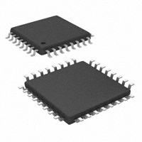
Package: 32-Pin TQFP
2 Applications
•
•
•
•
•
•
•
USB Headset
USB Headphone
USB Speaker
USB Featured Consumer Audio Product
USB Audio Interface Box
USB Monitor
Video Conference System
3 Description
The PCM2912A is the Texas Instruments single-chip,
USB stereo audio codec with a USB, 2.0-compliant,
full-speed protocol controller and an analog front-end
(AFE) function for headset applications.
The USB protocol controller works with no software
code, but USB descriptors can be modified on
request.
The
PCM2912A
employs
SpAct™
architecture, TI’s unique system that recovers the
audio clock from USB packet data. On-chip analog
PLLs with SpAct enables independent playback and
record sampling rates with low clock jitters.
Device Information(1)
PART NUMBER
PCM2912A
PACKAGE
TQFP (32)
BODY SIZE (NOM)
7.00 mm × 7.00 mm
(1) For all available packages, see the orderable addendum at
the end of the data sheet.
Block Diagram
USB
Mic Input
PCM2912A
VDD
VCCA
VCCR
VCCL
VCCP
Headphone
Play indicator
Record indicator
Suspend flag
PGND
HGND
BGND
AGND
DGND
An IMPORTANT NOTICE at the end of this data sheet addresses availability, warranty, changes, use in safety-critical applications,
intellectual property matters and other important disclaimers. PRODUCTION DATA.
�PCM2912A
SLES230A – SEPTEMBER 2008 – REVISED AUGUST 2015
www.ti.com
Table of Contents
1
2
3
4
5
6
7
8
9
Features ..................................................................
Applications ...........................................................
Description .............................................................
Revision History.....................................................
Device Comparison Table.....................................
Pin Configuration and Functions .........................
Specifications.........................................................
1
1
1
2
3
3
5
7.1
7.2
7.3
7.4
7.5
7.6
5
5
5
5
6
9
Absolute Maximum Ratings .....................................
ESD Ratings..............................................................
Recommended Operating Conditions.......................
Thermal Information ..................................................
Electrical Characteristics...........................................
Typical Characteristics ..............................................
Parameter Measurement Information ................ 14
Detailed Description ............................................ 15
9.1 Overview ................................................................. 15
9.2 Functional Block Diagram ....................................... 15
9.3 Feature Description................................................. 16
9.4 Device Functional Modes........................................ 19
9.5 Programming........................................................... 20
10 Application and Implementation........................ 24
10.1 Application Information.......................................... 24
10.2 Typical Application ............................................... 24
11 Power Supply Recommendations ..................... 27
12 Layout................................................................... 27
12.1 Layout Guidelines ................................................. 27
12.2 Layout Example .................................................... 27
13 Device and Documentation Support ................. 28
13.1
13.2
13.3
13.4
13.5
Documentation Support ........................................
Community Resources..........................................
Trademarks ...........................................................
Electrostatic Discharge Caution ............................
Glossary ................................................................
28
28
28
28
28
14 Mechanical, Packaging, and Orderable
Information ........................................................... 28
4 Revision History
NOTE: Page numbers for previous revisions may differ from page numbers in the current version.
Changes from Original (September 2008) to Revision A
•
2
Page
Added Pin Configuration and Functions section, ESD Ratings table, Feature Description section, Device Functional
Modes, Application and Implementation section, Power Supply Recommendations section, Layout section, Device
and Documentation Support section, Device Comparison table, and Mechanical, Packaging, and Orderable
Information section ................................................................................................................................................................ 1
Submit Documentation Feedback
Copyright © 2008–2015, Texas Instruments Incorporated
Product Folder Links: PCM2912A
�PCM2912A
www.ti.com
SLES230A – SEPTEMBER 2008 – REVISED AUGUST 2015
5 Device Comparison Table
FEATURE
PCM2900C
Supply voltage
5 V (Bus-Powered)
PCM2902C
Additional features
—
PCM2903C
PCM2906C
PCM2912A
5 V (Bus-Powered)
5 V (Bus-Powered)
S/PDIF I/O
500-mA Maximum
Power Configuration
Mic Bias
PGAs
Sidetone
5 V (Bus-Powered) 3.3 V (Bus-Powered)
S/PDIF I/O
S/PDIF I/O
6 Pin Configuration and Functions
POWER
MAMP
VOUTR
VCCR
HGND
VCCL
VOUTL
MBIAS
PJT Package
32-Pin TQFP
Top View
24
23
22
21
20
19
18
17
PGND
25
16
VIN
VCCP
26
15
VCCA
TEST1
27
14
NC
TEST0
28
13
AGND
VCOM2
PCM2912A
10
FR
PLAY
32
9
FL
1
2
3
4
5
6
7
8
XTI
31
XTO
REC
DGND
VCOM1
D+
11
VDD
30
D-
MMUTE
VBUS
29
BGND
SSPND
12
Pin Functions
PIN
NAME
NO.
I/O
DESCRIPTION
AGND
13
—
Analog ground
BGND
1
—
Reference for internal regulator
D–
3
I/O
USB differential input/output minus (1)
D+
4
I/O
USB differential input/output plus (1)
DGND
6
FL
9
—
External filter pin of L-channel (optional)
FR
10
—
External filter pin of R-channel (optional)
HGND
20
—
Analog ground for headphone amplifier
MAMP
23
I
Microphone preamplifier gain control (LOW: Preamplifier off, HIGH: Preamplifier on = +20 dB) (2)
MBIAS
17
O
Microphone bias output (0.75 VCCA)
MMUTE
30
I
Microphone mute control, active HIGH (LOW: Mute off, HIGH: Mute on) (3)
NC
14
—
(1)
(2)
(3)
Digital ground
Not connected
LV-TTL level
3.3-V CMOS level input.
3.3-V CMOS level input with internal pulldown resistor.
Submit Documentation Feedback
Copyright © 2008–2015, Texas Instruments Incorporated
Product Folder Links: PCM2912A
3
�PCM2912A
SLES230A – SEPTEMBER 2008 – REVISED AUGUST 2015
www.ti.com
Pin Functions (continued)
PIN
NAME
NO.
I/O
DESCRIPTION
PGND
25
—
Analog ground for microphone bias, microphone amplifier, and PGA
PLAY
32
O
Status output for playback (LOW: Playback, FLASH: Mute on playback, HIGH: Stop) (4)
POWER
24
I
Power consumption declaration select pin (LOW: 100 mA, HIGH: 500 mA)
REC
31
O
Status output for record (LOW: Record, FLASH: Mute on recode, HIGH: Stop) (4)
SSPND
29
O
Suspend flag (LOW: Suspend, HIGH: Operational state)
TEST0
28
I
Test pin. Must be set to LOW (2)
TEST1
27
I
Test pin. Must be set to HIGH (2)
VBUS
2
—
Connect to USB power (VBUS)
VCCA
15
—
Analog power supply
VCCL
19
—
Analog power supply for headphone amplifier of L-channel (5)
VCCP
26
—
Analog power supply for PLL (5)
VCCR
21
—
Analog power supply for headphone amplifier of R-channel (5)
VCOM1
11
—
Common voltage for ADC, DAC, and analog front-end (VCCA/2). Decoupling capacitor must be
connected to AGND.
VCOM2
12
—
Common voltage for headphone (VCCA/2). Decoupling capacitor must be connected to AGND.
VDD
5
—
Digital power supply (5)
VIN
16
I
ADC microphone input
VOUTL
18
O
Headphone output for L-channel
VOUTR
22
O
Headphone output for R-channel
XTI
8
I
Crystal oscillator input (2)
XTO
7
O
Crystal oscillator output
(4)
(5)
4
(2)
5-V tolerant, open-drain.
Connect decoupling capacitor to corresponding ground.
Submit Documentation Feedback
Copyright © 2008–2015, Texas Instruments Incorporated
Product Folder Links: PCM2912A
�PCM2912A
www.ti.com
SLES230A – SEPTEMBER 2008 – REVISED AUGUST 2015
7 Specifications
7.1 Absolute Maximum Ratings
Over operating free-air temperature range (unless otherwise noted). (1) (2)
MIN
MAX
UNIT
Supply voltage
VBUS
–0.3
6.5
V
Ground voltage
differences
BGND, PGND, AGND, HGND, DGND
–0.1
0.1
V
Input voltage
VCCP, VCCA, VCCL, VCCR, VDD
–0.3
4
V
PLAY, REC
–0.3
6.5
V
D+, D–, XTI, XTO, MMUTE, TEST0, TEST1, POWER, MAMP, SSPND
–0.3
4
V
MBIAS, VIN, VCOM1, VCOM2, VOUTL, VOUTR, FR, FL
–0.3
4
V
mA
Digital input voltage
Analog input voltage
Input current (any pins except supplies)
–10
10
Ambient temperature under bias
–40
125
Junction temperature
150
Storage temperature, Tstg
(1)
(2)
–55
°C
150
Stresses beyond those listed under Absolute Maximum Ratings may cause permanent damage to the device. These are stress ratings
only, and functional operation of the device at these or any other conditions beyond those indicated under Recommended Operating
Conditions is not implied. Exposure to absolute-maximum-rated conditions for extended periods may affect device reliability.
All voltage values are with respect to network ground terminal.
7.2 ESD Ratings
VALUE
V(ESD)
(1)
(2)
Electrostatic
discharge
Human body model (HBM), per ANSI/ESDA/JEDEC JS-001
(1)
UNIT
±3000
Charged device model (CDM), per JEDEC specification JESD22-C101 (2)
V
±1000
JEDEC document JEP155 states that 500-V HBM allows safe manufacturing with a standard ESD control process.
JEDEC document JEP157 states that 250-V CDM allows safe manufacturing with a standard ESD control process.
7.3 Recommended Operating Conditions
Over operating free-air temperature range (unless otherwise noted).
VBUS
Supply voltage
MIN
NOM
MAX
UNIT
4.35
5
5.25
V
Analog input voltage, full scale (–0 dB)
0.43 VCCA
Digital input logic family
Digital input clock frequency
5.997
Analog output load resistance
6
6.003
MHz
Ω
32
Analog output load capacitance
Digital output load capacitance
TA
VPP
TTL
Operating free-air temperature
–25
100
pF
10
pF
70
°C
7.4 Thermal Information
PCM2912A
THERMAL METRIC
(1)
PJT (TQFP)
UNIT
32 PINS
RθJA
Junction-to-ambient thermal resistance
69.6
°C/W
RθJC(top)
Junction-to-case (top) thermal resistance
10.6
°C/W
RθJB
Junction-to-board thermal resistance
34.6
°C/W
ψJT
Junction-to-top characterization parameter
0.3
°C/W
ψJB
Junction-to-board characterization parameter
33.9
°C/W
(1)
For more information about traditional and new thermal metrics, see the Semiconductor and IC Package Thermal Metrics application
report, SPRA953.
Submit Documentation Feedback
Copyright © 2008–2015, Texas Instruments Incorporated
Product Folder Links: PCM2912A
5
�PCM2912A
SLES230A – SEPTEMBER 2008 – REVISED AUGUST 2015
www.ti.com
7.5 Electrical Characteristics
All specifications at TA = 25°C, VBUS = 5 V, fS = 44.1 kHz, fIN = 1 kHz, and 16-bit data, unless otherwise noted. for Host
interface, apply USB revision 2.0, full-speed. For audio data format, use UsB isochronous data format.
PARAMETER
TEST CONDITIONS
MIN
TYP
MAX
UNIT
INPUT LOGIC
VIH
Input logic high level
VIL
Input logic low level
2
0.8
Input logic high current (1)
IIH
IIL
3.3
(2)
VIN = 3.3 V
–10
10
Input logic high current (3)
VIN = 3.3 V
Input logic low current (1)
VIN = 0 V
–10
10
VIN = 0 V
–10
10
Output logic high level (1)
IOH = –10 mA
2.9
Output logic high level (4)
IOH = –2 mA
2.8
Output logic low level (1)
Input logic low current
(2)
(3)
65
100
VDC
μA
μA
OUTPUT LOGIC
VOH
VOL
IOL = 10 mA
0.3
(4)
IOL = 2 mA
0.5
Output logic low level (5)
IOL = 8 mA
0.5
Output leak current (5)
VIN = 5 V
±10
Output logic low level
IOH
VDC
VDC
μA
CLOCK FREQUENCY
Input clock frequency, XTI
5.997
6.000
6.003
MHz
MICROPHONE BIAS
Output voltage
0.75 VCCA
Output current
Output noise
RL = 1 kΩ
VDC
2
mA
5
μVRMS
ANALOG-TO-DIGITAL CONVERTER (ADC) CHARACTERISTICS
Resolution
Audio data channel
16
Bits
1
Channel
8
11.025
16
22.05
32
44.1
48
Sampling frequency
kHz
ADC DYNAMIC PERFORMANCE (6)
THD+N
SNR
Total harmonic distortion plus noise
VIN = –1 dB of 0.43 VCCA
0.01%
0.02%
Dynamic range
A-weighted
82
90
dB
Signal-to-noise ratio
A-weighted
84
92
dB
ADC DC ACCURACY
Gain error
±2
Bipolar zero error
±0
±10
% of FSR
% of FSR
ANALOG INPUT
Input voltage
0.43 VCCA
Center voltage
Antialiasing filter frequency response
(1)
(2)
(3)
(4)
(5)
(6)
6
0.5 VCCA
–3 dB
fIN = 20 kHz
VPP
V
150
kHz
–0.08
dB
Pins 3, 4: D–, D+.
Pins 8, 23, 24, 27, 28: XTI, MAMP, POWER, TEST1, TEST0
Pin 30: MMUTE
Pins 7, 29: XTO, SSPND
Pins 31, 32: REC, PLAY.
fIN = 1 kHz, using Audio Precision™ System Two™, RMS mode with 20-kHz LPF, 400-Hz HPF in calculation. Microphone amplifier = 0
dB, PGA = 0 dB.
Submit Documentation Feedback
Copyright © 2008–2015, Texas Instruments Incorporated
Product Folder Links: PCM2912A
�PCM2912A
www.ti.com
SLES230A – SEPTEMBER 2008 – REVISED AUGUST 2015
Electrical Characteristics (continued)
All specifications at TA = 25°C, VBUS = 5 V, fS = 44.1 kHz, fIN = 1 kHz, and 16-bit data, unless otherwise noted. for Host
interface, apply USB revision 2.0, full-speed. For audio data format, use UsB isochronous data format.
PARAMETER
TEST CONDITIONS
MIN
TYP
MAX
UNIT
MICROPHONE AMPLIFIER
Gain
0
20
Input impedance
dB
20
kΩ
INPUT PGA
Gain range
–12
30
Gain step size
dB
1
dB
ADC DIGITAL FILTER PERFORMANCE
Passband
0.454 fS
Stop band
0.583 fS
Passband ripple
Hz
–0.02
Stop-band attenuation
0.02
dB
–65
Delay time
HPF frequency response
Hz
dB
17.4/fS
–3 dB
s
0.078 fS/1000
Hz
DIGITAL-TO-ANALOG CONVERTER (DAC) CHARACTERISTICS
Resolution
Audio data channel
16
Bits
1, 2
Channel
8
11.025
16
22.05
32
44.1
48
Sampling frequency
kHz
DAC DYNAMIC PERFORMANCE (7)
THD+N
SNR
Total harmonic distortion plus noise
RL > 10 kΩ, VOUT = 0 dB of 0.6 VCCA
RL = 32 Ω, VOUT = 0 dB of 0.55 VCCA
0.01%
0.02%
0.02%
0.05%
Dynamic range
EIAJ, A-weighted
82
90
dB
Signal-to-noise ratio
EIAJ, A-weighted
84
92
dB
Channel separation
RL > 10 kΩ
80
88
dB
Gain mismatch channel-to-channel
–10
±2
10
% of FSR
Gain error
–10
±2
10
% of FSR
DAC DC ACCURACY
Bipolar zero error
±3
% of FSR
ANALOG OUTPUT
Output voltage
RL > 10 kΩ
0.6 VCCA
RL = 32 Ω
0.55 VCCA
Center voltage
Output power
Load impedance (AC coupling)
LPF frequency response
(7)
0.5 VCCA
RL = 32 Ω
13
RL = 16 Ω
25
Line
10
Headphone
16
VPP
V
mW
kΩ
32
Ω
–3 dB
140
kHz
f = 20 kHz
–0.1
dB
fOUT = 1 kHz, using Audio Precision System Two, RMS mode with 20-kHz LPF, 400-Hz HPF. Output attenuator = 0 dB,
Sidetone = Mute.
Submit Documentation Feedback
Copyright © 2008–2015, Texas Instruments Incorporated
Product Folder Links: PCM2912A
7
�PCM2912A
SLES230A – SEPTEMBER 2008 – REVISED AUGUST 2015
www.ti.com
Electrical Characteristics (continued)
All specifications at TA = 25°C, VBUS = 5 V, fS = 44.1 kHz, fIN = 1 kHz, and 16-bit data, unless otherwise noted. for Host
interface, apply USB revision 2.0, full-speed. For audio data format, use UsB isochronous data format.
PARAMETER
TEST CONDITIONS
MIN
TYP
MAX
UNIT
SIDETONE PROGRAMMABLE ATTENUATOR
Gain range
–76
Gain step size
0
1
dB
dB
OUTPUT PROGRAMMABLE ATTENUATOR
Gain range
–76
Gain step size
0
1
dB
dB
ANALOG LOOPBACK PERFORMANCE (8)
THD+N
SNR
Total harmonic distortion plus noise
RL > 10 kΩ, VIN = 0 dB of 0.43 VCCA
RL = 32 Ω, VIN = 0 dB of 0.43 VCCA
0.01%
0.02%
0.02%
0.05%
Dynamic range
EIAJ, A-weighted
82
90
dB
Signal-to-noise ratio
EIAJ, A-weighted
84
92
dB
DAC DIGITAL FILTER PERFORMANCE
Passband
0.445 fS
Stop band
0.555 fS
Hz
Passband ripple
±0.1
Stop-band attenuation
–43
Delay time
Hz
dB
dB
14.3/fS
s
POWER-SUPPLY REQUIREMENTS
VBUS
Voltage range
Supply current
Power dissipation
Bus-powered
4.35
5
5.25
VDC
85
100
mA
Suspend mode (9)
220
300
μA
ADC, DAC Operation
425
500
mW
Suspend mode (9)
0.8
1
mW
3.3
3.6
VDC
85
°C
ADC, DAC operation (RL = 32 Ω)
VCCP,VCCL
Internally-generated power supply
VCCR,VCCA
voltage (10)
VDD
3
TEMPERATURE RANGE
Operation temperature
–25
(8) MIC Amp = 0 dB, Sidetone attenuator = 0 dB, Output attenuator = 0 dB.
(9) Under USB suspend state
(10) Pins 5, 15, 19, 21, 26: VDD, VCCA, VCCL, VCCR, VCCP.
8
Submit Documentation Feedback
Copyright © 2008–2015, Texas Instruments Incorporated
Product Folder Links: PCM2912A
�PCM2912A
www.ti.com
SLES230A – SEPTEMBER 2008 – REVISED AUGUST 2015
7.6 Typical Characteristics
7.6.1 ADC Digital Decimation Filter Frequency Response
All specifications at TA = 25°C, VBUS = 5 V, fS = 44.1 kHz, fIN = 1 kHz, and 16-bit data, unless otherwise noted.
0
0
-20
Amplitude - dB
Amplitude - dB
-40
-80
-40
-60
-120
-80
-100
-160
0
8
16
24
32
0
0.2
Normalized Frequency - x fS
Figure 1. Overall Characteristic
0.6
0.8
1.0
Figure 2. Stop Band Attenuation
0.2
0
0
-4
Amplitude - dB
Amplitude - dB
0.4
Normalized Frequency - x fS
-0.2
-0.4
-0.6
-8
-12
-16
-0.8
0
0.1
0.2
0.3
0.4
-20
0.46
0.5
0.48
0.50
0.52
0.54
Normalized Frequency - x fS
Normalized Frequency - x fS
Figure 3. Passband Ripple
Figure 4. Transient Band Response
7.6.2 ADC Digital High-Pass Filter Frequency Response
0
0
-20
-0.2
Amplitude - dB
Amplitude - dB
All specifications at TA = 25°C, VBUS = 5 V, fS = 44.1 kHz, fIN = 1 kHz, and 16-bit data, unless otherwise noted.
-40
-60
-0.4
-0.6
-0.8
-80
-100
-1.0
0
0.1
0.2
0.3
Normalized Frequency - x fS/1000
0.4
0
1
2
3
4
Normalized Frequency - x fS/1000
Figure 5. Stop Band Characteristic
Figure 6. Passband Characteristic
Submit Documentation Feedback
Copyright © 2008–2015, Texas Instruments Incorporated
Product Folder Links: PCM2912A
9
�PCM2912A
SLES230A – SEPTEMBER 2008 – REVISED AUGUST 2015
www.ti.com
7.6.3 ADC Analog Antialiasing Filter Frequency Response
0
0
-10
-0.2
Amplitude - dB
Amplitude - dB
All specifications at TA = 25°C, VBUS = 5 V, fS = 44.1 kHz, fIN = 1 kHz, and 16-bit data, unless otherwise noted.
-20
-30
-0.4
-0.6
-0.8
-40
-1.0
-50
1
10
100
1000
0.01
10000
0.1
1
10
100
f - Frequency - kHz
f - Frequency - kHz
Figure 7. Stop Band Characteristic
Figure 8. Passband Characteristic
7.6.4 DAC Digital Interpolation Filter Frequency Response
0
0.2
-20
0
Amplitude - dB
Amplitude - dB
All specifications at TA = 25°C, VBUS = 5 V, fS = 44.1 kHz, fIN = 1 kHz, and 16-bit data, unless otherwise noted.
-40
-60
-0.2
-0.4
-0.6
-80
-100
-0.8
0
1
2
3
0
4
0.1
0.2
0.3
0.4
Normalized Frequency - x fS
Normalized Frequency - x fS
Figure 9. Stop Band Attenuation
Figure 10. Passband Ripple
0.5
0
Amplitude - dB
-4
-8
-12
-16
-20
0.46
0.48
0.50
0.52
0.54
Normalized Frequency - x fS
Figure 11. Transient Band Response
10
Submit Documentation Feedback
Copyright © 2008–2015, Texas Instruments Incorporated
Product Folder Links: PCM2912A
�PCM2912A
www.ti.com
SLES230A – SEPTEMBER 2008 – REVISED AUGUST 2015
7.6.5 DAC Analog FIR Filter Frequency Response
0
0.2
-10
0
Amplitude - dB
Amplitude - dB
All specifications at TA = 25°C, VBUS = 5 V, fS = 44.1 kHz, fIN = 1 kHz, and 16-bit data, unless otherwise noted.
-20
-30
-40
-0.2
-0.4
-0.6
-50
-0.8
0
8
16
24
32
0
0.1
0.2
0.3
0.4
0.5
Normalized Frequency - x fS
Normalized Frequency - x fS
Figure 12. Stop Band Characteristic
Figure 13. Passband Characteristic
7.6.6 DAC Analog Low-Pass Filter Frequency Response
0
0
-10
-0.2
Amplitude - dB
Amplitude - dB
All specifications at TA = 25°C, VBUS = 5 V, fS = 44.1 kHz, fIN = 1 kHz, and 16-bit data, unless otherwise noted.
-20
-30
-40
-0.4
-0.6
-0.8
-50
-1.0
1
10
100
10000
1000
0.01
0.1
f - Frequency - kHz
1
10
100
f - Frequency - kHz
Figure 14. Stop Band Characteristic
Figure 15. Passband Characteristic
7.6.7 ADC
All specifications at TA = 25°C, VBUS = 5 V, fS = 44.1 kHz, fIN = 1 kHz, and 16-bit data, unless otherwise noted.
96
0.009
Dynamic Range and SNR - dB
THD+N - Total Harmonic Distortion + Noise - %
0.010
0.008
0.007
0.006
0.005
94
SNR
92
Dynamic Range
90
88
0.004
0.003
-50
86
-25
0
25
50
75
100
-50
TA - Free-Air Temperature - °C
Figure 16. THD+N at –1 dB vs Temperature
-25
0
25
50
75
TA - Free-Air Temperature - °C
100
Figure 17. Dynamic Range and Signal-to-Noise Ratio vs
Temperature
Submit Documentation Feedback
Copyright © 2008–2015, Texas Instruments Incorporated
Product Folder Links: PCM2912A
11
�PCM2912A
SLES230A – SEPTEMBER 2008 – REVISED AUGUST 2015
www.ti.com
ADC (continued)
All specifications at TA = 25°C, VBUS = 5 V, fS = 44.1 kHz, fIN = 1 kHz, and 16-bit data, unless otherwise noted.
98
0.009
96
Dynamic Range and SNR - dB
THD+N - Total Harmonic Distortion + Noise - %
0.010
0.008
0.007
0.006
0.005
SNR
92
Dynamic Range
90
88
0.004
0.003
4.2
94
4.4
4.6
4.8
5.0
5.2
86
4.2
5.4
4.4
VBUS - Supply Voltage - V
Figure 18. THD+N at –1 dB vs Supply Voltage
4.8
5.0
5.2
5.4
Figure 19. Dynamic Range and Signal-to-Noise Ratio vs
Supply Voltage
0.010
98
0.009
96
Dynamic Range and SNR - dB
THD+N - Total Harmonic Distortion + Noise - %
4.6
VBUS - Supply Voltage - V
0.008
0.007
0.006
0.005
94
SNR
92
90
Dynamic Range
88
0.004
0.003
30
35
40
45
86
30
50
35
40
45
50
fS - Sampling Frequency - kHz
fS - Sampling Frequency - kHz
Figure 20. THD+N at –1 dB vs Sampling Frequency
Figure 21. Dynamic Range and Signal-to-Noise Ratio vs
Sampling Frequency
7.6.8 DAC
All specifications at TA = 25°C, VBUS = 5 V, fS = 44.1 kHz, fIN = 1 kHz, and 16-bit data, unless otherwise noted.
96
0.009
94
Dynamic Range and SNR - dB
THD+N - Total Harmonic Distortion + Noise - %
0.010
0.008
0.007
0.006
0.005
Dynamic Range
90
88
0.004
86
-50
0.003
-50
-25
0
25
50
75
100
-25
0
25
50
75
100
TA - Free-Air Temperature - °C
TA - Free-Air Temperature - °C
Figure 22. THD+N at 0 dB vs Temperature
12
SNR
92
Figure 23. Dynamic Range and Signal-to-Noise Ratio vs
Temperature
Submit Documentation Feedback
Copyright © 2008–2015, Texas Instruments Incorporated
Product Folder Links: PCM2912A
�PCM2912A
www.ti.com
SLES230A – SEPTEMBER 2008 – REVISED AUGUST 2015
DAC (continued)
0.010
98
0.009
96
Dynamic Range and SNR - dB
THD+N - Total Harmonic Distortion + Noise - %
All specifications at TA = 25°C, VBUS = 5 V, fS = 44.1 kHz, fIN = 1 kHz, and 16-bit data, unless otherwise noted.
0.008
0.007
0.006
0.005
94
SNR
92
Dynamic Range
90
88
0.004
86
0.003
4.2
4.4
4.6
4.8
5.0
5.2
4.2
5.4
0.010
98
0.009
96
0.008
0.007
0.006
0.005
0.004
0.003
35
40
45
4.6
4.8
5.0
5.2
5.4
Figure 25. Dynamic Range and Signal-to-Noise Ratio vs
Supply Voltage
Dynamic Range and SNR - dB
THD+N - Total Harmonic Distortion + Noise - %
Figure 24. THD+N at 0 dB vs Supply Voltage
30
4.4
VBUS - Supply Voltage - V
VBUS - Supply Voltage - V
94
SNR
92
Dynamic Range
90
88
86
30
50
35
40
45
50
fS - Sampling Frequency - kHz
fS - Sampling Frequency - kHz
Figure 26. THD+N at 0 dB vs Sampling Frequency
Figure 27. Dynamic Range and Signal-to-Noise Ratio vs
Sampling Frequency
7.6.9 Supply Current
All specifications at TA = 25°C, VBUS = 5 V, fS = 44.1 kHz, fIN = 1 kHz, and 16-bit data, unless otherwise noted.
100
0.4
90
Operational Current
80
0.3
Suspend Current
70
0.2
60
0.1
50
4.2
4.4
4.6
4.8
5.0
5.2
0
5.4
Operational Current - mA
Operational Current - mA
90
0.5
Suspend Current - mA
100
80
70
60
50
30
35
40
45
50
fS - Sampling Frequency - kHz
VBUS - Supply Voltage - V
Figure 28. Supply Current vs Supply Voltage
Figure 29. Supply Current vs Sampling Frequency
Submit Documentation Feedback
Copyright © 2008–2015, Texas Instruments Incorporated
Product Folder Links: PCM2912A
13
�PCM2912A
SLES230A – SEPTEMBER 2008 – REVISED AUGUST 2015
www.ti.com
Supply Current (continued)
All specifications at TA = 25°C, VBUS = 5 V, fS = 44.1 kHz, fIN = 1 kHz, and 16-bit data, unless otherwise noted.
0.40
Suspend Current - mA
0.35
USB spec limit for device = 0.3 mA
0.30
0.25
0.20
0.15
0.10
-40
0
-20
20
40
60
80
100
TA - Free-Air Temperature - °C
Figure 30. Supply Current vs Temperature at Suspend Mode
8 Parameter Measurement Information
All parameters are measured according to the conditions described in Specifications.
14
Submit Documentation Feedback
Copyright © 2008–2015, Texas Instruments Incorporated
Product Folder Links: PCM2912A
�PCM2912A
www.ti.com
SLES230A – SEPTEMBER 2008 – REVISED AUGUST 2015
9 Detailed Description
9.1 Overview
The PCM2912A is an audio codec with USB connection capability and an analog front-end for headset
applications.
The PCM2912A is a bus-powered device that uses the USB voltage source. The PCM2912A meets the
requirements of USB2.0 standard connection. This device has analog and digital inputs and outputs; it has a
digital USB interface for input and output data; the analog input is directly routed to the A/D converter and to the
analog output. The microphone input has an optional mic amp with fixed +20 dB. The PCM2912A has 2 digital
output flags that can be used as LED indicators for Playback and Record. The PCM2912A requires a 12-MHz
clock; it can be provided by an external clock or generated by a built-in crystal resonator.
9.2 Functional Block Diagram
BGND
VCCA/VCCP/VCCL/VCCR/VDD
VREF
5 V to 3.3 V
Voltage
Regulator
AGND/ HGND/ PGND/DGND
Power
Manager
SSPND
VBUS
MIC
BIAS
MBIAS
VIN
MIC
AMP
PGA + 30 dB ~ –12 dB
in 1 dB steps
FIFO
ADC
+20/0 dB
ISO-In
Endpoint
XCVR
D+
D–
Selector
USB SIE
Analog
PLL
VCOM2
VCOM1
S
FL
MMUTE
PLAY
Selector
DAC
VOUTR
FIFO
S
HP AMP 15 mW (at 32 W)
ATT 0 dB ~ –76 dB
in 1 dB steps with Mute
ISO-Out
Endpoint
USB Protocol
Controller
FR
PLL (x16)
POWER
MAMP
Analog
PLL
ATT 0 dB ~ –76 dB
in 1 dB steps with Mute
VOUTL
Control
Endpoint
96 MHz
REC
TEST0
TEST1
Tracker
(SpAct® )
6.000 MHz
XTI
XTO
Submit Documentation Feedback
Copyright © 2008–2015, Texas Instruments Incorporated
Product Folder Links: PCM2912A
15
�PCM2912A
SLES230A – SEPTEMBER 2008 – REVISED AUGUST 2015
www.ti.com
9.3 Feature Description
9.3.1 Clock and Reset
The PCM2912A requires a 6-MHz (±500 ppm) clock for USB function and audio function, which can be
generated from a built-in crystal oscillator with a 6-MHz crystal resonator. The 6-MHz crystal resonator must be
connected to XTI (pin 8) and XTO (pin 7) with one high (1-MΩ) resistor and two small capacitors, whose
capacitance depends on the load capacitance of the crystal resonator. An external clock can be supplied through
XTI; if an external clock is supplied, XTO must be left open. Because there is no clock disabling signal, using the
external clock supply is not recommended. SSPND (pin 29) is unable to use clock disabling.
The PCM2912A has an internal power-on-reset circuit, which works automatically when VBUS (pin 2) exceeds
2.5 V, typical (2.2 V to 2.7 V), and approximately 700 μs is required until the internal reset is released.
9.3.2 DAC
The PCM2912A has a stereo delta-sigma DAC that uses a 64-fS oversampling technique with an 8-fS
oversampling digital filter. DAC outputs are provided through the headphone amplifier; VOUTL (pin 18) and VOUTR
(pin 22) provide 13 mW at 32 Ω and 0.6 VCCL/VCCR VPP at a 10-kΩ load.
9.3.3 ADC
The PCM2912A has a mono delta-sigma ADC that uses a 64-fS oversampling technique with a 1/64-fS
decimation digital filter. The microphone input, VIN (pin 16), is fed to the ADC through a +20-dB microphone
amplifier and the PGA, which has +30 dB to –12 dB in 1-dB steps.
9.3.4 Microphone Bias
The PCM2912A has a microphone bias generator, which provides a low-noise, 0.75-VCCA, 2-mA source current
output with appropriate output impedance for electret-microphone driving. This output, MBIAS (pin 17), should be
bypassed to AGND (pin 13) through an appropriate capacitor to reduce the output noise level.
9.3.5 Microphone Amplifier
The PCM2912A has a low-noise, single-ended, mono microphone amplifier with a mute function that is controlled
by MUTE (pin 30). The signal gain is selectable by MAMP (pin 23). The noise level at the input node is 5 μVRMS,
and the input impedance is 20 kΩ.
9.3.6 Input PGA
The PCM2912A also has a low-noise input, programmable gain amplifier (PGA) for the microphone amplifier
output/ADC input, with a gain range of +30 dB to –12 dB in 1dB/step.
9.3.7 Sidetone Programmable Attenuator
The PCM2912A has a low-noise, sidetone programmable attenuator with a mute function for the sidetone signal
path (microphone amplifier output to output PGA input), and a gain range of 0 dB to –76 dB in 1 dB/step.
9.3.8 Output Programmable Attenuator
The PCM2912A has a low-noise output programmable attenuator with a mute function for mixed signal, which
affects DAC output signal and sidetone signal. The output PGA gain range is 0 dB to –76 dB in 1 dB/step.
9.3.9 VCOM1 and VCCM2
VCOM2 (pin 12) is provided for the center voltage of the headphone amplifier. VCOM1 (pin 11) is provided for the
center voltage of all other analog circuits. Each VCOM pin must be decoupled with an appropriate capacitor.
Because the headphone output is disconnected when entering the suspend state, determining the capacitance is
important to prevent pop noise, especially for VCOM2 (pin 12). The equivalent resistance of VCOM2 is 500 kΩ, and
VCOM1 is 15 kΩ.
16
Submit Documentation Feedback
Copyright © 2008–2015, Texas Instruments Incorporated
Product Folder Links: PCM2912A
�PCM2912A
www.ti.com
SLES230A – SEPTEMBER 2008 – REVISED AUGUST 2015
Feature Description (continued)
9.3.10 Filter Pins
FL (pin 9) and FR (pin 10) are provided to make a low-pass filter (LPF) to decrease the DAC outband noise, as
shown in Figure 31. This filter is optional.
Side Tone
20 kW
20 kW
10 kW
10 kW
DAC
–
+
VCOM
FR/FL
CF
Figure 31. Filter Circuit
9.3.11 Interface Sequence
9.3.11.1 Power-On, Attach, and Play Back Sequence
The PCM2912A is ready for setup when the reset sequence has finished and the USB bus is attached. After a
connection has been established, the PCM2912A is ready to accept USB audio data. While waiting for the audio
data (that is, in an idle state), the analog output is set to bipolar zero (BPZ).
When receiving the audio data, the PCM2912A stores the first audio packet, which contains 1-ms audio data,
into the internal storage buffer. The PCM2912A starts playing the audio data when the subsequent Start of
Frame (SOF) packet is detected, as shown in Figure 32.
Submit Documentation Feedback
Copyright © 2008–2015, Texas Instruments Incorporated
Product Folder Links: PCM2912A
17
�PCM2912A
SLES230A – SEPTEMBER 2008 – REVISED AUGUST 2015
www.ti.com
Feature Description (continued)
5.0 V (typ)
2.5 V (typ)
VBUS (pin 2)
0V
Bus Reset
D+ (pin 4),
D- (pin 3)
1st Audio Data
Set Configuration
2nd Audio Data
Bus Idle
SOF
SOF
SOF
SSPND (pin 29)
VOUTL (pin 18),
VOUTR (pin 22)
700 ms
Device Setup
1 ms
Internal Reset
Ready for Setup
Ready for Playback
Figure 32. Initial Sequence
9.3.11.2 Play, Stop, and Detach Sequence
When the host finishes or aborts the play back process, the PCM2912A stops playing after last audio data has
played, as shown in Figure 33.
VBUS (pin 2)
Audio Data
Audio Data
Last Audio Data
D+ (pin 4),
D- (pin 3)
SOF
SOF
SOF
SOF
SOF
VOUTL (pin 18),
VOUTR (pin 22)
1 ms
Detach
Figure 33. Play, Stop, and Detach
18
Submit Documentation Feedback
Copyright © 2008–2015, Texas Instruments Incorporated
Product Folder Links: PCM2912A
�PCM2912A
www.ti.com
SLES230A – SEPTEMBER 2008 – REVISED AUGUST 2015
Feature Description (continued)
9.3.11.3 Record Sequence
Figure 34 illustrates how the PCM2912A records the audio into the internal memory after receiving the
SET_INTERFACE command.
SET_INTERFACE
IN token
Audio data
IN token
Audio data
IN token
Audio data
D+ (pin 4),
D– (pin 3)
SOF
SOF
SOF
SOF
SOF
VIN (pin 16)
1ms
Figure 34. Record Sequence
9.3.11.4 Suspend and Resume Sequence
The PCM2912A enters a suspend state when it sees a constant idle state on the USB bus after approximately
5 ms. When the PCM2912A enters the suspend state, the SSPND flag (pin 29) is asserted. The PCM2912A
wakes up immediately after detecting the non-idle state on the USB bus. Figure 35 illustrates these actions.
Idle
D+ (pin 4),
D- (pin 3)
SSPND (pin 29)
5 ms
Suspend
VOUTL (pin 18),
VOUTR (pin 22)
Active
Active
2.5 ms
Figure 35. Suspend and Resume
9.4 Device Functional Modes
The PCM2912A is a USB-controlled device. The PCM2912A is a codec, with an analog input (that goes to an
A/D converter) and analog output (that comes from a D/A converter), alongside the analog path that goes from
the microphone input to the headphone output. A wider explanation of these operational modes is shown in
Feature Description.
The PCM2912A has hardware controls to turn on and off the integrated microphone preamplifier and the
microphone input itself (MAMP and MMUTE, respectively); the microphone preamplifier has +20-dB fixed gain.
Submit Documentation Feedback
Copyright © 2008–2015, Texas Instruments Incorporated
Product Folder Links: PCM2912A
19
�PCM2912A
SLES230A – SEPTEMBER 2008 – REVISED AUGUST 2015
www.ti.com
9.5 Programming
9.5.1 USB Interface
Control data and audio data are transferred to the PCM2912A via D+ (pin 4) and D– (pin 3). All data transferred
to/from the PCM2912A are performed at full speed. Table 1 summarizes the device descriptor. The device
descriptor can be modified on request.
Table 1. Device Descriptor
DEVICE DESCRIPTOR
DESCRIPTION
USB revision
2.0 compliant
Device class
0x00 (device defined in interface level)
Device sub class
0x00 (not specified)
Device protocol
0x00 (not specified)
Maximum packet size for endpoint 0
8-byte
Vendor ID
0x08BB
Product ID
0x2912
Device release number
0x0100 (1.00)
Number of configurations
1
Vendor string
String #1 (refer to Table 3)
Product string
String #2 (refer to Table 3)
Serial number
Not supported
Table 2 lists the configuration descriptor. The configuration descriptor can be modified on request.
Table 2. Configuration Descriptor
CONFIGURATION DESCRIPTOR
DESCRIPTION
Interface
Three interfaces
Power attribute
0x80 (Bus powered, no remote wakeup)
Max power
0x32 (100 mA at POWER = Low) / 0xFA (500mA at POWER = High)
Table 3 summarizes the string descriptor. The string descriptor can be modified on request.
Table 3. String Descriptor
20
STRING DESCRIPTOR
DESCRIPTION
#0
0x0409
#1
Burr-Brown from TI
#2
USB audio CODEC
Submit Documentation Feedback
Copyright © 2008–2015, Texas Instruments Incorporated
Product Folder Links: PCM2912A
�PCM2912A
www.ti.com
SLES230A – SEPTEMBER 2008 – REVISED AUGUST 2015
9.5.1.1 Device Configuration
Figure 36 illustrates the USB audio function topology. The PCM2912A has three interfaces. Each interface is
constructed with some alternative settings.
Endpoint #0
Default Endpoint
FU
Endpoint #1
(IF #1)
IT
S
OT
TID3
UID4
TID6
Audio Streaming Interface
Analog Out
UID5
FU
IT
TID1
UID2
Analog In
FU
Endpoint #1
(IF #1)
OT
S
IT
TIDB
UIDA
TID7
Audio Streaming Interface
UID8
Standard Audio Control Interface (IF #0)
Figure 36. USB Audio Function Topology
9.5.1.2 Interface #0
Interface #0 is the control interface. Alternative setting #0 is the only possible setting for interface #0. Alternative
setting #0 describes the standard audio control interface. The audio control interface is constructed with a series
of terminal connections. The PCM2912A has the following 10 terminals:
• Input terminal (Terminal ID#1) for audio analog input for sidetone
• Feature unit (Unit ID#2) for sidetone PGA
• Input terminal (Terminal ID#3) for isochronous out stream
• Mixer unit (Unit ID#4) for sidetone mixing
• Feature unit (Unit ID#5) for analog output PGA
• Output terminal (Terminal ID#6) for audio analog output
• Input terminal (Terminal ID#7) for audio analog input
• Feature unit (Unit ID#8) for analog input PGA
• Mixer unit (Unit ID#A) for analog input
• Output terminal (Terminal ID#B) for isochronous in stream
Submit Documentation Feedback
Copyright © 2008–2015, Texas Instruments Incorporated
Product Folder Links: PCM2912A
21
�PCM2912A
SLES230A – SEPTEMBER 2008 – REVISED AUGUST 2015
www.ti.com
Input terminal #3 is defined as USB stream (terminal type 0x0101). Input terminal #3 can accept two-channel
audio streams constructed by the left and right channels. Output terminal #6 is defined as a speaker (terminal
type 0x0301). Input terminals #1 and #7 are defined as Microphone (terminal type 0x0201). Physically, these two
input terminals are the same input, but logically duplicated. Output terminal B is defined as a USB stream
(terminal type 0x0101). Output terminal B is a single-channel audio stream. Mixer unit #4 multiplexes the analog
input (sidetone) and the audio data of the digital-to-analog converter (DAC). Mixer unit A is placed in front of
output terminal B. Mixer unit A has no impact on recording data. Mixer units #4 and A do not have programming
capability.
Feature unit #5 supports the following sound control features for analog outputs:
• Volume control
• Mute control
The built-in volume controller can be manipulated by an audio-class-specific request from 0 dB to –76 dB in
steps of 1 dB. An individual (L and R) channel can be set for different values. The built-in mute controller can be
manipulated by an audio-class-specific request. Only the master mute control request is acceptable.
Feature unit #2 supports the following sound control features for analog input (sidetone):
• Volume control
• Mute control
The built-in volume controller can be manipulated by an audio-class-specific request from 0 dB to –76 dB in 1-dB
steps. Only the master volume control is acceptable. The built-in mute controller can be manipulated by audioclass-specific request. Only the master mute control request is acceptable.
Feature unit #8 supports the following sound control features for analog input (microphone record input):
• Volume control
• Mute control
The built-in analog volume controller can be manipulated by an audio-class-specific request from +30 dB to –12
dB in 1-dB steps. The built-in mute controller can be manipulated by an audio-class-specific request. Only the
master mute control request is acceptable.
9.5.1.3 Interface #1
Interface #1 is the audio streaming interface for data output. Table 4 lists the three alternative settings for
Interface #1. Alternative setting #0 is the zero bandwidth setting. All other alternative settings are operational
settings.
Table 4. Interface #1 Alternative Settings
ALTERNATIVE
SETTING
DATA FORMAT
00
TRANSFER MODE
SAMPLING RATE (kHz)
Zero Bandwidth
01
16 bit
Stereo
2s complement (PCM)
Adaptive
8, 11.025, 16, 22.05, 32, 44.1,
48
02
16 bit
Mono
2s complement (PCM)
Adaptive
8, 11.025, 16, 22.05, 32, 44.1,
48
9.5.1.4 Interface #2
Interface #2 is the audio streaming interface for data output. Table 5 shows the two alternative settings for
Interface #2. Alternative setting #0 is the Zero Band Width setting. Alternative setting #1 is an operational setting.
Table 5. Interface #2 Alternative Settings
ALTERNATIVE
SETTING
DATA FORMAT
00
01
22
TRANSFER MODE
SAMPLING RATE (kHz)
Zero Bandwidth
16 bit
Mono
2s complement (PCM)
Submit Documentation Feedback
Asynchronous
8, 11.025, 16, 22.05, 32,
44.1, 48
Copyright © 2008–2015, Texas Instruments Incorporated
Product Folder Links: PCM2912A
�PCM2912A
www.ti.com
SLES230A – SEPTEMBER 2008 – REVISED AUGUST 2015
9.5.1.5 Endpoints
The PCM2912A has the following three endpoints:
• Control endpoint (EP #0)
• Isochronous out audio data stream endpoint (EP #1)
• Isochronous in audio data stream endpoint (EP #2)
The control endpoint is the default endpoint. The control endpoint controls all functions of the PCM2912A by the
standard USB request and USB audio class-specific request from the host. The isochronous out audio data
stream endpoint is an audio sink endpoint, which receives the PCM audio data. The isochronous out audio data
stream endpoint accepts the asynchronous transfer mode. The isochronous in audio data stream endpoint is an
audio source endpoint, which transmits the PCM audio data. The isochronous in audio data stream endpoint
uses synchronous transfer mode.
9.5.1.6 Internal Regulator
All required power sources are generated by five internal regulators.
Each regulator generates 3.3 V (typical, without load) from VBUS (pin 2). Each regulator has an output pin and a
ground return pin (as described in Table 6); this pair must be decoupled with an appropriate capacitor. Note that
this capacitance affects inrush-current limitation. One band-gap reference circuit supplies reference voltage for all
regulators. BGND (pin 1) is provided for reference ground of the band-gap reference.
Table 6. Internal Regulator Summary
SUPPLIED CIRCUIT
OUTPUT
RETURN
Digital
VDD (pin 5)
DGND (pin 6)
Analog
VCCA (pin 15)
AGND (pin 13)
Headphone (L-ch)
VCCL (pin 19)
HGND (pin 20)
Headphone (R-ch)
VCCR (pin 21)
HGND (pin 20)
PLL
VCCP (pin 26)
PGND (pin 25)
Submit Documentation Feedback
Copyright © 2008–2015, Texas Instruments Incorporated
Product Folder Links: PCM2912A
23
�PCM2912A
SLES230A – SEPTEMBER 2008 – REVISED AUGUST 2015
www.ti.com
10 Application and Implementation
NOTE
Information in the following applications sections is not part of the TI component
specification, and TI does not warrant its accuracy or completeness. TI’s customers are
responsible for determining suitability of components for their purposes. Customers should
validate and test their design implementation to confirm system functionality.
10.1 Application Information
The VBUS alerts the device when it has been plugged to a USB connection port. The /SSPND flag notifies when
the USB input is idle for at least 5 ms; this flag can be used to control or notify subsequent circuits. More
functional details can be found in Interface Sequence.
10.2 Typical Application
A bus-powered (Hi-power), +20-dB microphone amplifier application example is shown in Figure 37.
Headphone
Microphone
R11
R8
R10
R7
R5
C13
C16
C10
27
TEST1
28
TEST0
29
SSPND
30
MMUTE
31
REC
32
PLAY
VOUTR
4
5
PLAY
R2
C6
FR 10
C5
6
7
8
C1
R1
C7
XTI
3
VCOM2 12
DGND
2
1
C18
REC
C8
VCOM1 11
XTO
VDD
BGND
VIN 16
AGND 13
PCM2912A
D+
R1 3
17 MBIAS
NC 14
D-
R1 2
18
VCCA 15
VBUS
Mic Mute
19
VCCL
MAMP
VCCP
20
VOUTL
PGND
26
21
VCCR
25
C17
22
HGND
23
C9
C11
C14
POWER 24
FL
9
C4
R4
X1
R3
C2
C3
L1
V BUS D–
D+ GND
USB Connector
NOTE: X1: 6-MHz crystal resonator
C1, C8, C11, C14, C17, C18: 1 μF ceramic
C2, C3: 10 pF to 33 pF (depending on load capacitance of crystal resonator)
C4, C5: 100 pF ceramic
C6, C10: 3.3 μF
C7: 0.1 μF
C9: 0.22 μF electrolytic (depending on required frequency response for microphone input)
C13, C16: 100 μF electrolytic (depending on required frequency response for headphone output)
R1, R2: 22 Ω to 33 Ω
R3: 1.5 kΩ
R4: 1 MΩ
R5: 1 kΩ (depending on microphone characteristic)
R7, R8, R10, R11: 3.3 kΩ
R12, R13: 820 Ω (depending on LED drive current)
L1: 1 μH (DC resistance < 0.6 Ω)
It is possible to change maximum power if total power of actual application does not require over 100 mA (set
POWER = low to configure as low-power device).
Figure 37. USB Headset Application
24
Submit Documentation Feedback
Copyright © 2008–2015, Texas Instruments Incorporated
Product Folder Links: PCM2912A
�PCM2912A
www.ti.com
SLES230A – SEPTEMBER 2008 – REVISED AUGUST 2015
Typical Application (continued)
NOTE
The circuit in Figure 37 is for information only. Total board design should be considered in
order to meet the USB specification as a USB-compliant product.
10.2.1 Design Requirements
For this design example, use the parameters listed in Table 7.
Table 7. Design Parameters
DESIGN PARAMETER
EXAMPLE VALUE
Input voltage range
4.35 V to 5.25 V
Current
80 mA to 100 mA
Input clock frequency
11.994 MHz to 12.006 MHz
10.2.2 Detailed Design Procedure
The PCM2912A is a simple design device, as can connect directly to a USB port. The device only requires
decoupling capacitors on the voltage source pins and the output filter for the headphone amplifier; a
recommended output filter is the one implemented in the PCM2912AEVM, shown in the user's guide (SBAU141).
10.2.3 Application Curves
For the application curves, see the graphs listed in Table 8.
Table 8. Table of Graphs
FIGURE
ADC Digital Decimation Filter Frequency
Response
Overall Characteristic
Figure 1
Stop Band Attenuation
Figure 2
Passband Ripple
Figure 3
Transient Band Response
Figure 4
ADC Digital High-Pass Filter Frequency
Response
Stop Band Characteristic
Figure 5
Passband Characteristic
Figure 6
ADC Analog Antialiasing Filter Frequency
Response
Stop Band Characteristic
Figure 7
Passband Characteristic
Figure 8
DAC Digital Interpolation Filter Frequency
Response
DAC Analog FIR Filter Frequency Response
DAC Analog Low-Pass Filter Frequency
Response
ADC
Stop Band Attenuation
Figure 9
Passband Ripple
Figure 10
Transient Band Response
Figure 11
Stop Band Characteristic
Figure 12
Passband Characteristic
Figure 13
Stop Band Characteristic
Figure 14
Passband Characteristic
Figure 15
THD+N at – 1 dB vs Temperature
Figure 16
Dynamic Range and Signal-to-Noise Ratio vs Temperature
Figure 17
THD+N at – 1 dB vs Supply Voltage
Figure 18
Dynamic Range and Signal-to-Noise Ratio vs Supply Voltage
Figure 19
THD+N at – 1 dB vs Sampling Frequency
Figure 20
Dynamic Range and Signal-to-Noise Ratio vs Sampling
Frequency
Figure 21
Submit Documentation Feedback
Copyright © 2008–2015, Texas Instruments Incorporated
Product Folder Links: PCM2912A
25
�PCM2912A
SLES230A – SEPTEMBER 2008 – REVISED AUGUST 2015
www.ti.com
Table 8. Table of Graphs (continued)
FIGURE
DAC
Supply Current
26
THD+N at 0 dB vs Temperature
Figure 22
Dynamic Range and Signal-to-Noise Ratio vs Temperature
Figure 23
THD+N at 0 dB vs Supply Voltage
Figure 24
Dynamic Range and Signal-to-Noise Ratio vs Supply Voltage
Figure 25
THD+N at 0 dB vs Sampling Frequency
Figure 26
Dynamic Range and Signal-to-Noise Ratio vs Sampling
Frequency
Figure 27
Supply Current vs Supply Voltage
Figure 28
Supply Current vs Sampling Frequency
Figure 29
Supply Current vs Temperature at Suspend Mode
Figure 30
Submit Documentation Feedback
Copyright © 2008–2015, Texas Instruments Incorporated
Product Folder Links: PCM2912A
�PCM2912A
www.ti.com
SLES230A – SEPTEMBER 2008 – REVISED AUGUST 2015
11 Power Supply Recommendations
The voltage source to power the PCM2912A must be between 4.35 V and 5.25 V for proper operation (USB
voltage). TI recommends placing a decoupling capacitor in every voltage source pin to help filter lower frequency
power supply noise. Place these decoupling capacitors as close as possible to the PCM2912A.
12 Layout
12.1 Layout Guidelines
The decoupling capacitors must be as close as possible to the PCM2912A pins. TI recommends following the
output filter for the headphone amplifier used in the PCM2912A EVM. The analog input needs a series capacitor
to eliminate any possible offset level. The PCM2912A is a low-power device, thus there is no need for a special
heat sink PCB design.
12.2 Layout Example
820Ω
1uF
820Ω
16Ω
3.3KΩ
0.022uF
3.3KΩ
100uF
1uF
VOUT R
DD+
VBUS
GND
33Ω
VOUT L
PCM2912A
33Ω
1uF
1uF
0.022uF
3.3KΩ
100uF
3.3KΩ
1uF
1.5KΩ
16Ω
USB port
10uF
1KΩ
3.3uF
100pF
10uF
1MΩ
Clock hardware for
built-in resonator
100pF
0.1uF
6MHz
22pF
Analog Input
1uF
Decoupling capacitors as
close as possible to de IC
22pF
Connection to ground plane
Top layer traces
Top layer ground plane
Submit Documentation Feedback
Copyright © 2008–2015, Texas Instruments Incorporated
Product Folder Links: PCM2912A
27
�PCM2912A
SLES230A – SEPTEMBER 2008 – REVISED AUGUST 2015
www.ti.com
13 Device and Documentation Support
13.1 Documentation Support
13.1.1 Related Documentation
For related documentation, see the following:
• Operating Envronments for PCM2912 Applications, SLAA387
• EVM User's Guide, SBAU141
13.2 Community Resources
The following links connect to TI community resources. Linked contents are provided "AS IS" by the respective
contributors. They do not constitute TI specifications and do not necessarily reflect TI's views; see TI's Terms of
Use.
TI E2E™ Online Community TI's Engineer-to-Engineer (E2E) Community. Created to foster collaboration
among engineers. At e2e.ti.com, you can ask questions, share knowledge, explore ideas and help
solve problems with fellow engineers.
Design Support TI's Design Support Quickly find helpful E2E forums along with design support tools and
contact information for technical support.
13.3 Trademarks
SpAct, E2E are trademarks of Texas Instruments.
Audio Precision, System Two are trademarks of Audio Precision, Inc..
All other trademarks are the property of their respective owners.
13.4 Electrostatic Discharge Caution
These devices have limited built-in ESD protection. The leads should be shorted together or the device placed in conductive foam
during storage or handling to prevent electrostatic damage to the MOS gates.
13.5 Glossary
SLYZ022 — TI Glossary.
This glossary lists and explains terms, acronyms, and definitions.
14 Mechanical, Packaging, and Orderable Information
The following pages include mechanical, packaging, and orderable information. This information is the most
current data available for the designated devices. This data is subject to change without notice and revision of
this document. For browser-based versions of this data sheet, refer to the left-hand navigation.
28
Submit Documentation Feedback
Copyright © 2008–2015, Texas Instruments Incorporated
Product Folder Links: PCM2912A
�PACKAGE OPTION ADDENDUM
www.ti.com
10-Dec-2020
PACKAGING INFORMATION
Orderable Device
Status
(1)
Package Type Package Pins Package
Drawing
Qty
Eco Plan
(2)
Lead finish/
Ball material
MSL Peak Temp
Op Temp (°C)
Device Marking
(3)
(4/5)
(6)
PCM2912APJT
ACTIVE
TQFP
PJT
32
250
RoHS & Green
NIPDAU
Level-1-260C-UNLIM
-25 to 85
PCM2912A
PCM2912APJTR
ACTIVE
TQFP
PJT
32
1000
RoHS & Green
NIPDAU
Level-1-260C-UNLIM
-25 to 85
PCM2912A
(1)
The marketing status values are defined as follows:
ACTIVE: Product device recommended for new designs.
LIFEBUY: TI has announced that the device will be discontinued, and a lifetime-buy period is in effect.
NRND: Not recommended for new designs. Device is in production to support existing customers, but TI does not recommend using this part in a new design.
PREVIEW: Device has been announced but is not in production. Samples may or may not be available.
OBSOLETE: TI has discontinued the production of the device.
(2)
RoHS: TI defines "RoHS" to mean semiconductor products that are compliant with the current EU RoHS requirements for all 10 RoHS substances, including the requirement that RoHS substance
do not exceed 0.1% by weight in homogeneous materials. Where designed to be soldered at high temperatures, "RoHS" products are suitable for use in specified lead-free processes. TI may
reference these types of products as "Pb-Free".
RoHS Exempt: TI defines "RoHS Exempt" to mean products that contain lead but are compliant with EU RoHS pursuant to a specific EU RoHS exemption.
Green: TI defines "Green" to mean the content of Chlorine (Cl) and Bromine (Br) based flame retardants meet JS709B low halogen requirements of