�������
�� ��
�����
�
� � ��� ������� ���
PCM3060
SLAS533B – MARCH 2007 – REVISED MARCH 2008
24-BIT, 96/192-kHz ASYNCHRONOUS STEREO AUDIO CODEC
FEATURES
1
•
•
•
•
•
•
24-Bit Delta-Sigma ADC and DAC
ADC, DAC Asynchronous Operation
Stereo ADC:
– High Performance: (Typical, 48 kHz)
– THD+N: –93 dB
– SNR: 99 dB
– Dynamic Range: 99 dB
– Sampling Rate: 16–96 kHz
– System Clock: 256, 384, 512, 768 fS
– Full Scale Input: 3 Vp-p
– Antialiasing Filter Included
– 1/64 Decimation Filter:
– Pass-Band Ripple: ±0.05 dB
– Stop-Band Attenuation: –65 dB
– On-Chip High-Pass Filter: 0.91 Hz at
fS = 48 kHz
Stereo DAC:
– High Performance: (Typical, Differential,
48 kHz)
– THD+N: –94 dB
– SNR: 105 dB
– Dynamic Range: 104 dB
– Sampling Rate: 16–192 kHz
– System Clock: 128, 192, 256, 384,
512, 768 fS
– Differential Voltage Output: 8 Vp-p
– Single-Ended Voltage Output: 4 Vp-p
– Analog Low-Pass Filter Included
– 4×/8× Oversampling Digital Filter:
– Pass-Band Ripple: ±0.04 dB
– Stop-Band Attenuation: –50 dB
– Zero Flags
Flexible Mode Control
– 3-Wire SPI, 2-Wire I2C Compatible Serial
Control Interface
– Hardware Control Mode
Multiple Functions via SPI or I2C Interface:
– Digital Attenuation and Soft Mute for ADC
•
•
•
•
•
and DAC
– Digital De-Emphasis: 32, 44.1, 48 kHz for
DAC
– Power Down: ADC/DAC Independently
– Asynchronous/Synchronous Control for
ADC/DAC Operation
External Reset and Power-Down Pin:
– ADC/DAC Simultaneously
Audio Interface Mode:
– ADC/DAC Independent Master/Slave
Audio Data Format:
– ADC/DAC Independent
– I2S, Left-Justified, Right-Justified
Dual Power Supplies:
– 5-V for Analog and 3.3-V for Digital
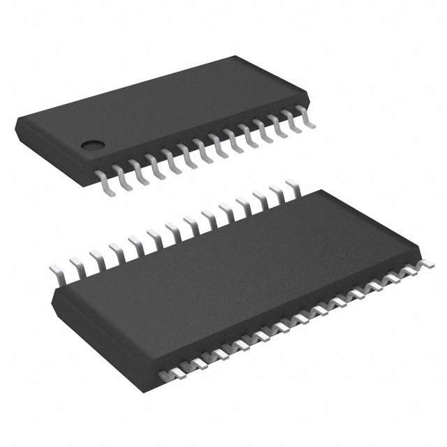
Package: TSSOP-28
APPLICATIONS
•
•
•
•
DVD-RW
Digital TV
Digital Set-Top Box
Audio-Visual Applications
DESCRIPTION
The PCM3060 is a low-cost, high-performance,
single-chip, 24-bit stereo audio codec with
single-ended analog inputs and differential analog
outputs.
The stereo 24-bit ADC employs a 64-times
delta-sigma modulator. It supports 16–96 kHz
sampling rates and a 16/24-bit digital audio output
word on the audio interface.
The stereo 24-bit DAC employs a 64- or 128-times
delta-sigma modulator. It supports 16–192 kHz
sampling rates and a 16/24-bit digital audio input
word on the audio interface.
The PCM3060 supports fully independent operation
of the sampling rate and audio interface for the ADC
and DAC.
Each audio interface supports I2S, left-justified, and
right-justified formats with 16/24-bit words.
1
Please be aware that an important notice concerning availability, standard warranty, and use in critical applications of
Texas Instruments semiconductor products and disclaimers thereto appears at the end of this data sheet.
PRODUCTION DATA information is current as of publication date.
Products conform to specifications per the terms of the Texas
Instruments standard warranty. Production processing does not
necessarily include testing of all parameters.
Copyright © 2007–2008, Texas Instruments Incorporated
�PCM3060
www.ti.com
SLAS533B – MARCH 2007 – REVISED MARCH 2008
This integrated circuit can be damaged by ESD. Texas Instruments recommends that all integrated circuits be handled with
appropriate precautions. Failure to observe proper handling and installation procedures can cause damage.
ESD damage can range from subtle performance degradation to complete device failure. Precision integrated circuits may be more
susceptible to damage because very small parametric changes could cause the device not to meet its published specifications.
DESCRIPTION (CONTINUED)
The PCM3060 can be software-controlled through a 3-wire SPI-compatible or 2-wire I2C-compatible serial
interface, which provides access to all functions including digital attenuation, soft mute, de-emphasis etc.
The PCM3060 can be also used in hardware mode, which provides three basic functions.
The PCM3060 is fabricated using a highly advanced CMOS process and is available in a small 28-pin TSSOP
package.
The PCM3060 is suitable for various sound processing applications for DVD-RW, digital TV, STB, and other AV
equipment.
ABSOLUTE MAXIMUM RATINGS
over operating free-air temperature range (unless otherwise noted)
(1)
VALUE
Supply voltage
Ground voltage differences
–0.3 to 6.5
VDD
–0.3 to 4
AGND1, AGND2, DGND, SGND
RST, MS, MC, MD, SCKI1, SCKI2, DIN
Digital input voltage
Analog input voltage
UNIT
VCC
V
±0.1
V
–0.3 to 6.5
V
BCK1, BCK2, LRCK1, LRCK2, DOUT
–0.3 to (VDD + 0.3 V) < 4
V
ZEROL, ZEROR, MODE
–0.3 to (VDD + 0.3 V) < 4
V
VINL, VINR, VCOM, VOUTL+, VOUTL–, VOUTR+, VOUTR–
–0.3 to (VCC + 0.3 V) < 6.5
V
±10
mA
Input current (any pins except supplies)
TA
Ambient temperature under bias
–40 to 125
°C
Tstg
Storage temperature
–55 to 150
°C
TJ
Junction temperature
150
°C
260, 5 s
°C
260
°C
Lead temperature (soldering)
Package temperature (IR reflow, peak)
(1)
Stresses beyond those listed under absolute maximum ratings may cause permanent damage to the device. These are stress ratings
only and functional operation of the device at these or any other conditions beyond those indicated under recommended operating
conditions is not implied. Exposure to absolute-maximum-rated conditions for extended periods may affect device reliability.
RECOMMENDED OPERATING CONDITIONS
over operating free-air temperature range (unless otherwise noted)
MIN
NOM
MAX
VCC
Analog supply voltage
4.5
5
5.5
V
VDD
Digital supply voltage
2.7
3.3
3.6
V
Digital input interface level
Digital input clock frequency
TTL compatible
Sampling frequency, LRCK1, LRCK2
System clock frequency, SCKI1, SCKI2
16
2.048
Analog input level
Analog output load resistance
96/192
kHz
36.864
MHz
3
AC-coupled
5
DC-coupled
10
Vpp
kΩ
kΩ
Analog output load capacitance
50
pF
Digital output load capacitance
20
pF
85
°C
Operating free-air temperature
2
UNIT
–25
Submit Documentation Feedback
25
Copyright © 2007–2008, Texas Instruments Incorporated
Product Folder Link(s): PCM3060
�PCM3060
www.ti.com
SLAS533B – MARCH 2007 – REVISED MARCH 2008
ELECTRICAL CHARACTERISTICS
All specifications at TA = 25°C, VCC = 5 V, VDD = 3.3 V, fS = 48 kHz, SCKI1 = SCKI2 = 512 fS, 24-bit data (unless otherwise
noted).
PARAMETER
TEST CONDITIONS
PCM3060PW
MIN
TYP
UNIT
MAX
DIGITAL INPUT/OUTPUT
DATA FORMAT
I2S, LJ, RJ
Audio data interface format
Audio data word length
16, 24
Audio data format
fS
Bits
MSB-first, 2s-complement
Sampling frequency, ADC
16
48
96
Sampling frequency, DAC
16
48
192
System clock frequency
128, 192, 256, 384, 512, 768 fS
2.048
36.864
2
VDD
kHz
MHz
INPUT LOGIC
VIH
(1)
VIL
(1)
VIH
(2) (3)
0.8
Input logic level
2
VIL (2) (3)
0.8
IIH (2)
IIL (2)
IIH
(1) (3)
VDC
5.5
Input logic current
IIL (1) (3)
VIN = VDD
±10
VIN = 0 V
±10
VIN = VDD
65
VIN = 0 V
µA
100
±10
OUTPUT LOGIC
VOH
(4)
(4) (5)
VOL
Output logic level
IOUT = –4 mA
2.8
IOUT = 4 mA
VDC
0.5
REFERENCE OUTPUT
VCOM output voltage
0.5 VCC
VCOM output impedance
7
12.5
Allowable VCOM output
source/sink current
V
18
kΩ
±1
µA
ADC CHARACTERISTICS
Resolution
16
24
Bits
0.6 VCC
Vp-p
ANALOG INPUT
Full scale input voltage
VINL, VINR = 0 dB
Center voltage
0.5 VCC
Input impedance
Antialiasing filter response
–3 dB
V
10
kΩ
300
kHz
DC ACCURACY
(1)
(2)
(3)
(4)
(5)
Gain mismatch,
channel-to-channel
Full-scale input, VINL, VINR
Gain error
Full-scale input, VINL, VINR
Bipolar zero error
HPF bypass, VINL, VINR
±2
±8
% of FSR
±2
±8
% of FSR
±0.5
±2
% of FSR
BCK1, BCK2, LRCK1, LRCK2 (in slave mode, Schmitt-trigger input with 50-kΩ typical internal pulldown resistor)
SCKI1, SCKI2, DIN, MS/ADR/IFMD, MC/SCL/FMT, MD/SDA/IFMD (Schmitt-trigger input, 5-V tolerant).
RST (Schmitt-trigger input with 50-kΩ typical internal pulldown resistor, 5-V tolerant).
BCK1, BCK2, LRCK1, LRCK2 (in master mode), DOUT, ZEROL, ZEROR
MD/SDA/IFMD (in I2C mode, open drain LOW output)
Submit Documentation Feedback
Copyright © 2007–2008, Texas Instruments Incorporated
Product Folder Link(s): PCM3060
3
�PCM3060
www.ti.com
SLAS533B – MARCH 2007 – REVISED MARCH 2008
ELECTRICAL CHARACTERISTICS (continued)
All specifications at TA = 25°C, VCC = 5 V, VDD = 3.3 V, fS = 48 kHz, SCKI1 = SCKI2 = 512 fS, 24-bit data (unless otherwise
noted).
PARAMETER
DYNAMIC PERFORMANCE
THD+N
PCM3060PW
MIN
TYP
MAX
VIN = –1 dB, fS = 48 kHz
–93
–85
VIN = –1 dB, fS = 96 kHz
–93
UNIT
(6) (7)
Total harmonic distortion + noise
Dynamic range
SNR
TEST CONDITIONS
Signal-to-noise ratio
Channel separation
(between L-ch and R-ch)
Crosstalk from DAC
fS = 48 kHz, A-weighted
95
fS = 96 kHz, A-weighted
fS = 48 kHz, A-weighted
95
dB
99
dB
101
92
fS = 96 kHz
fS1 = 48 kHz, fS2 = 44.1 kHz
99
101
fS = 96 kHz, A-weighted
fS = 48 kHz
dB
96
dB
98
92
fS1 = 96 kHz, fS2 = 44.1 kHz
96
dB
98
DIGITAL FILTER PERFORMANCE
0.454
fS
Pass band
0.583
fS
Stop band
Pass-band ripple
< 0.454 fS
Stop-band attenuation
> 0.583 fS
Hz
±0.05
dB
–65
Group delay time
HPF frequency response
Hz
–3 dB
dB
17.4/fS
s
0.019 fS
/1000
Hz
24
Bits
DAC CHARACTERISTICS
Resolution
16
ANALOG OUTPUT
Output voltage
Center voltage
Load impedance
LPF frequency response
Single-ended
0.8 VCC
Differential
1.6 VCC
Single-ended
0.5 VCC
Differential
V
0.48 VCC
AC-coupled
5
DC-coupled
10
kΩ
f = 20 kHz
–0.02
f = 44 kHz
–0.07
–3 dB
Vp-p
dB
300
kHz
DC ACCURACY
Gain mismatch,
channel-to-channel
±1
±4
% of FSR
Gain error
±2
±6
% of FSR
Single-ended
±1
±2
Differential (VOUTX+ – VOUTX–)
±1
Bipolar zero error
(6)
(7)
4
% of FSR
fIN = 1 kHz, using System Two audio measurement system by Audio Precision, RMS mode with 20-kHz LPF and 400-Hz HPF.
fS = 96 kHz: SCKI1 = SCKI2 = 256 fS, fS = 192 kHz: SCKI1 = 512 fS at fS = 48 kHz and SCKI2 = 128 fS at fS = 192 kHz.
Submit Documentation Feedback
Copyright © 2007–2008, Texas Instruments Incorporated
Product Folder Link(s): PCM3060
�PCM3060
www.ti.com
SLAS533B – MARCH 2007 – REVISED MARCH 2008
ELECTRICAL CHARACTERISTICS (continued)
All specifications at TA = 25°C, VCC = 5 V, VDD = 3.3 V, fS = 48 kHz, SCKI1 = SCKI2 = 512 fS, 24-bit data (unless otherwise
noted).
PARAMETER
PCM3060PW
TYP
MAX
VOUT = 0 dB, fS = 48 kHz
–93
–85
Total harmonic distortion + noise VOUT = 0 dB, fS = 96 kHz
–94
DYNAMIC PERFORMANCE (SINGLE-ENDED)
THD+N
TEST CONDITIONS
MIN
(8) (9) (10)
VOUT = 0 dB, fS = 192 kHz
fS = 48 kHz, EIAJ, A-weighted
Dynamic range
Signal-to-noise ratio
103
103
DYNAMIC PERFORMANCE (DIFFERENTIAL)
THD+N
104
fS = 192 kHz, EIAJ, A-weighted
104
97
101
fS = 192 kHz
101
101
fS1 = 48 kHz, fS2 = 176.4 kHz
101
–95
Crosstalk from ADC
VOUT = 0 dB, fS = 192 kHz
–95
fS = 48 kHz, EIAJ, A-weighted
104
fS = 96 kHz, EIAJ, A-weighted
104
fS = 192 kHz, EIAJ, A-weighted
104
fS = 48 kHz, EIAJ, A-weighted
105
fS = 96 kHz, EIAJ, A-weighted
105
fS = 192 kHz, EIAJ, A-weighted
105
fS = 48 kHz
103
fS = 96 kHz
103
fS = 192 kHz
103
fS1 = 48 kHz, fS2 = 44.1 kHz
103
fS1 = 48 kHz, fS2 = 88.2 kHz
103
fS1 = 48 kHz, fS2 = 176.4 kHz
103
DIGITAL FILTER PERFORMANCE
dB
dB
dB
dB
dB
SHARP ROLLOFF
0.454
fS
Pass band
0.546
fS
Stop band
(8)
(9)
(10)
(11)
dB
(8) (9) (11)
–94
Channel separation
dB
101
fS1 = 48 kHz, fS2 = 88.2 kHz
VOUT = 0 dB, fS = 48 kHz
Signal-to-noise ratio
dB
101
fS = 96 kHz
97
dB
104
Total harmonic distortion + noise VOUT = 0 dB, fS = 96 kHz
Dynamic range
SNR
100
fS = 96 kHz, EIAJ, A-weighted
fS1 = 48 kHz, fS2 = 44.1 kHz
Crosstalk from ADC
103
fS = 192 kHz, EIAJ, A-weighted
fS = 48 kHz
Channel separation
dB
–94
99
fS = 96 kHz, EIAJ, A-weighted
fS = 48 kHz, EIAJ, A-weighted
SNR
UNIT
Pass-band ripple
< 0.454 fS
Stop-band attenuation
> 0.546 fS
Hz
Hz
±0.04
–50
dB
dB
fS = 96 kHz: SCKI1 = SCKI2 = 256 fS, fS = 192 kHz: SCKI1 = 512 fS at fS = 48 kHz and SCKI2 = 128 fS at fS = 192 kHz.
fOUT = 1 kHz, using System Two audio measurement system by Audio Precision, RMS mode with 20-kHz LPF and 400-Hz HPF.
Assumed 5-kΩ AC-coupled second-order LPF and 115-dB or higher- performance buffer.
Assumed 10-kΩ DC-coupled second-order LPF and 115- dB or higher-performance differential to single-ended converter.
Submit Documentation Feedback
Copyright © 2007–2008, Texas Instruments Incorporated
Product Folder Link(s): PCM3060
5
�PCM3060
www.ti.com
SLAS533B – MARCH 2007 – REVISED MARCH 2008
ELECTRICAL CHARACTERISTICS (continued)
All specifications at TA = 25°C, VCC = 5 V, VDD = 3.3 V, fS = 48 kHz, SCKI1 = SCKI2 = 512 fS, 24-bit data (unless otherwise
noted).
PARAMETER
TEST CONDITIONS
DIGITAL FILTER PERFORMANCE
PCM3060PW
MIN
TYP
MAX
UNIT
SLOW ROLLOFF
0.308
fS
Pass band
Stop band
0.73 fS
Pass-band ripple
< 0.308 fS
Stop-band attenuation
> 0.73 fS
Hz
Hz
±0.5
–35
dB
dB
DIGITAL FILTER PERFORMANCE
Group delay time
20/fS
s
De-emphasis error
±0.1
dB
POWER SUPPLY REQUIREMENTS
VCC
VDD
4.5
5
5.5
2.7
3.3
3.6
fS = 48 kHz/ADC, fS = 48 kHz/DAC
25
36
fS = 96 kHz/ADC, fS = 96 kHz/DAC
25
mA
fS1 = 48 kHz/ADC, fS2 = 192 kHz/DAC
25
mA
fS = 48 kHz/ADC, power down/DAC
12
mA
Power down/ADC, fS = 48 kHz/DAC
13
mA
Voltage range
ICC
Supply current
IDD
Full power down
mA
µA
780
fS = 48 kHz/ADC, fS = 48 kHz/DAC
9
fS = 96 kHz/ADC, fS = 96 kHz/DAC
16
mA
fS1 = 48 kHz/ADC, fS2 = 192 kHz/DAC
12
mA
13
mA
fS = 48 kHz/ADC, power down/DAC
5
mA
Power down/ADC, fS = 48 kHz/DAC
5
mA
Full power down
Power dissipation
(12) (13)
VDC
(12)
µA
150
fS = 48 kHz/ADC, fS = 48 kHz/DAC
160
fS = 96 kHz/ADC, fS = 96 kHz/DAC
180
fS1 = 48 kHz/ADC, fS2 = 192 kHz/DAC
170
fS = 48 kHz/ADC, power down/DAC
220
mW
77
Power down/ADC, fS = 48 kHz/DAC
82
Full power down (12) (13)
4.4
TEMPERATURE RANGE
Operation temperature
θJA
–25
Thermal resistance
85
105
°C
°C/W
(12) Halt SCKI1, SCKI2, BCK1, BCK2, LRCK1, LRCK2
(13) AC-coupled configuration. If DC-coupled configuration is used, DC current flow to external load is added and it depends on external load
resistance.
6
Submit Documentation Feedback
Copyright © 2007–2008, Texas Instruments Incorporated
Product Folder Link(s): PCM3060
�PCM3060
www.ti.com
SLAS533B – MARCH 2007 – REVISED MARCH 2008
PIN ASSIGNMENTS
PCM3060
PW (TSSOP) PACKAGE
(TOP VIEW)
MC/SCL/FMT
MD/SDA/DEMP
DOUT
LRCK1
BCK1
SCKI1
VDD
DGND
SCKI2
BCK2
LRCK2
DIN
ZEROR
ZEROL
1
2
3
4
5
6
7
8
9
10
11
12
13
14
28
27
26
25
24
23
22
21
20
19
18
17
16
15
MODE
MS/ADR/IFMD
VINR
VINL
VCC
AGND1
AGND2
VCOM
VOUTL+
VOUTL–
VOUTR+
VOUTR–
SGND
RST
P0043-03
Submit Documentation Feedback
Copyright © 2007–2008, Texas Instruments Incorporated
Product Folder Link(s): PCM3060
7
�PCM3060
www.ti.com
SLAS533B – MARCH 2007 – REVISED MARCH 2008
Table 1. TERMINAL FUNCTIONS
TERMINAL
I/O
DESCRIPTION
NAME
PIN
AGND1
23
–
ADC analog ground
AGND2
22
–
DAC analog ground
5
I/O (1)
Audio data bit clock input/output for ADC
BCK2
10
(1)
I/O
Audio data bit clock input/output for DAC
DGND
8
–
12
I (2)
Audio data digital input for DAC
Audio data digital output for ADC
BCK1
DIN
Digital ground
DOUT
3
O
LRCK1
4
I/O(1)
Audio data left/right clock input/output for ADC
LRCK2
11
I/O(1)
Audio data left/right clock input/output for DAC
MC/SCL/FMT
MD/SDA/DEMP
1
(2)
I
(3)
2
I/O
MODE
28
I
MS/ADR/IFMD
27
I (2)
RST
15
I
(4)
Mode control, clock for SPI, clock for I2C, format for H/W mode(5)
Mode control, data for SPI, data for I2C, de-emphasis for H/W mode
This pin provides four operation modes according to its input connection. Connected directly to
VDD: SPI mode. Connected to VDD through 220-kΩ pullup resistor: H/W mode, single-ended
VOUTX. Connected to DGND through 220-kΩ pulldown resistor: H/W mode, differential VOUTX.
Connected directly to DGND : I2C mode.
Mode control, select for SPI with low active, address for I2C, I/F mode for H/W mode
(5)
Reset and power-down control input, active-low
(2)
System clock input for ADC
System clock input for DAC
SCKI1
6
I
SCKI2
9
I(2)
SGND
16
–
Shield analog ground
VCC
24
–
ADC, DAC analog power supply, 5-V
VCOM
21
–
ADC, DAC voltage common decoupling
VDD
7
–
Digital power supply, 3.3-V
VINL
25
I
Analog input to ADC, L-channel
VINR
26
I
Analog input to ADC, R-channel
VOUTL–
19
O
Analog output from DAC, L-channel – in differential mode, must be open in single-ended mode
VOUTL+
20
O
Analog output from DAC, L-channel + in differential mode, L-channel in single-ended mode
ZEROL
14
O
Zero flag, L-channel
ZEROR
13
O
Zero flag, R-channel
VOUTR–
17
O
Analog output from DAC, R-channel – in differential mode, must be open in single-ended mode
VOUTR+
18
O
Analog output from DAC, R-channel + in differential mode, R-channel in single-ended mode
(1)
(2)
(3)
(4)
(5)
8
Schmitt-trigger input/output with 50-kΩ typical internal pulldown resistor
Schmitt-trigger input, 5-V tolerant
Schmitt-trigger input, 5 V tolerant for SPI, H/W mode and Schmitt-trigger input/open drain LOW output, 5-V tolerant for I2C
VDD/2 biased, quad-state input
Schmitt-trigger input with 50-kΩ typical internal pulldown resistor, 5-V tolerant
Submit Documentation Feedback
Copyright © 2007–2008, Texas Instruments Incorporated
Product Folder Link(s): PCM3060
�PCM3060
www.ti.com
SLAS533B – MARCH 2007 – REVISED MARCH 2008
BLOCK DIAGRAM
VINL
SE to Diff.
Converter
Delta-Sigma
Modulator
VDD
Decimation Filter
with HPF
VINR
SE to Diff.
Converter
DGND
Delta-Sigma
Modulator
DOUT
LRCK1
VCC
AGND1
SGND
AGND2
Common
and
Reference
Voltage Common and Reference
VCOM
Audio
Interface
and
Clock
Control
ZEROR
VOUTR–
VOUTR+
VOUTL–
SCK1
SCK2
BCK2
LRCK2
LPF and
Buffer
Multi-Level
Delta-Sigma
Modulator
DIN
RST
Interpolation Filter
with Digital Function
VOUTL+
BCK1
LPF and
Buffer
Multi-Level
Delta-Sigma
Modulator
MODE
Mode
Control
MS/ADR/IFMD
MC/SCL/FMT
MD/SDA/DEMP
ZEROL
B0229-01
Submit Documentation Feedback
Copyright © 2007–2008, Texas Instruments Incorporated
Product Folder Link(s): PCM3060
9
�PCM3060
www.ti.com
SLAS533B – MARCH 2007 – REVISED MARCH 2008
TYPICAL PERFORMANCE CURVES OF ADC INTERNAL FILTER
All specifications at TA = 25°C, VCC = 5 V, VDD = 3.3 V, fS = 48 kHz, SCKI1 = SCKI2 = 512 fS, 24-bit data,
unless otherwise noted.
DIGITAL FILTER
DECIMATION FILTER, STOP-BAND CHARACTERISTICS
DECIMATION FILTER, PASS-BAND CHARACTERISTICS
0.1
0
−20
0.0
Amplitude − dB
Amplitude − dB
−40
−60
−80
−100
−0.1
−0.2
−0.3
−120
−0.4
−140
−160
0
8
16
24
−0.5
0.0
32
Normalized Frequency [×fS]
0.1
0.2
0.3
0.4
Normalized Frequency [×fS]
G001
Figure 1.
0.5
G002
Figure 2.
ANALOG FILTER
ANTIALIASING FILTER CHARACTERISTICS
0
−5
−5
−10
−10
−15
−15
Amplitude − dB
Amplitude − dB
HIGH-PASS FILTER CHARACTERISTICS
0
−20
−25
−30
−20
−25
−30
−35
−35
−40
−40
−45
−45
−50
0.0
−50
0.1
0.2
0.3
0.4
Normalized Frequency [×fS/1000]
1
100
1k
10k
f − Frequency − kHz
G004
G003
Figure 3.
10
10
Figure 4.
Submit Documentation Feedback
Copyright © 2007–2008, Texas Instruments Incorporated
Product Folder Link(s): PCM3060
�PCM3060
www.ti.com
SLAS533B – MARCH 2007 – REVISED MARCH 2008
TYPICAL PERFORMANCE CURVES OF DAC INTERNAL FILTER
All specifications at TA = 25°C, VCC = 5 V, VDD = 3.3 V, fS = 48 kHz, SCKI1 = SCKI2 = 512 fS, 24-bit data,
unless otherwise noted.
DIGITAL FILTER
INTERPOLATION FILTER, STOP BAND
(SHARP-ROLL OFF)
INTERPOLATION FILTER, PASS BAND
(SHARP-ROLL OFF)
0.1
0
−20
0.0
Amplitude − dB
Amplitude − dB
−40
−60
−80
−100
−0.1
−0.2
−0.3
−120
−0.4
−140
−160
0
1
2
3
−0.5
0.0
4
Normalized Frequency [×fS]
0.1
0.2
0.3
0.4
Normalized Frequency [×fS]
G005
Figure 5.
0.5
G006
Figure 6.
ANALOG FILTER
DE-EMPHASIS FILTER CHARACTERISTICS
(fS = 44.1 kHz)
LOW-PASS FILTER CHARACTERISTICS
0
0
−1
−2
−10
Amplitude − dB
Amplitude − dB
−3
−4
−5
−6
−20
−30
−7
−8
−40
−9
−10
−50
0
2
4
6
8
10
12
14
16
18
20
1
10
100
1k
10k
f − Frequency − kHz
f − Frequency − kHz
G008
G007
Figure 7.
Figure 8.
Submit Documentation Feedback
Copyright © 2007–2008, Texas Instruments Incorporated
Product Folder Link(s): PCM3060
11
�PCM3060
www.ti.com
SLAS533B – MARCH 2007 – REVISED MARCH 2008
TYPICAL ADC PERFORMANCE CURVES
All specifications at TA = 25°C, VCC = 5 V, VDD = 3.3 V, fS = 48 kHz, SCKI1 = SCKI2 = 512 fS, 24-bit data,
unless otherwise noted.
−88
104
VIN = –0.5 dB
−90
102
−92
−94
−96
−98
−100
−25
Dynamic Range
100
98
SNR
96
94
0
25
50
75
TA − Free-Air Temperature − °C
92
−25
100
G009
25
50
75
100
G010
Figure 9.
Figure 10.
THD+N at –1 dB vs SUPPLY VOLTAGE
DYNAMIC RANGE and SNR vs SUPPLY VOLTAGE
−88
104
VIN = –1 dB
−90
102
−92
−94
−96
−98
−100
4.50
100
Dynamic Range
SNR
98
96
94
4.75
5.00
5.25
VCC − Supply Voltage − V
5.50
92
4.50
G011
Figure 11.
12
0
TA − Free-Air Temperature − °C
Dynamic Range and SNR − dB
THD+N − Total Harmonic Distortion + Noise − dB
DYNAMIC RANGE and SNR vs TEMPERATURE
Dynamic Range and SNR − dB
THD+N − Total Harmonic Distortion + Noise − dB
THD+N at –1 dB vs TEMPERATURE
4.75
5.00
5.25
VCC − Supply Voltage − V
5.50
G012
Figure 12.
Submit Documentation Feedback
Copyright © 2007–2008, Texas Instruments Incorporated
Product Folder Link(s): PCM3060
�PCM3060
www.ti.com
SLAS533B – MARCH 2007 – REVISED MARCH 2008
TYPICAL DAC PERFORMANCE CURVES
All specifications at TA = 25°C, VCC = 5 V, VDD = 3.3 V, fS = 48 kHz, SCKI1 = SCKI2 = 512 fS, 24-bit data,
unless otherwise noted.
DYNAMIC RANGE and SNR vs TEMPERATURE
−90
110
−92
108
Dynamic Range and SNR − dB
THD+N − Total Harmonic Distortion + Noise − dB
THD+N vs TEMPERATURE
−94
−96
−98
−100
−102
−25
0
25
50
75
Dynamic Range
102
98
−25
100
0
25
50
75
100
TA − Free-Air Temperature − °C
G013
G014
Figure 13.
Figure 14.
THD+N vs SUPPLY VOLTAGE
DYNAMIC RANGE and SNR vs SUPPLY VOLTAGE
−90
110
−92
108
Dynamic Range and SNR − dB
THD+N − Total Harmonic Distortion + Noise − dB
104
100
TA − Free-Air Temperature − °C
−94
−96
−98
−100
−102
4.50
SNR
106
106
SNR
104
Dynamic Range
102
100
4.75
5.00
5.25
VCC − Supply Voltage − V
5.50
98
4.50
G015
Figure 15.
4.75
5.00
5.25
VCC − Supply Voltage − V
5.50
G016
Figure 16.
Submit Documentation Feedback
Copyright © 2007–2008, Texas Instruments Incorporated
Product Folder Link(s): PCM3060
13
�PCM3060
www.ti.com
SLAS533B – MARCH 2007 – REVISED MARCH 2008
TYPICAL PERFORMANCE CURVES
All specifications at TA = 25°C, VCC = 5 V, VDD = 3.3 V, fS = 48 kHz, SCKI1 = SCKI2 = 512 fS, 24-bit data,
unless otherwise noted.
ADCs OUTPUT SPECTRUM
OUTPUT SPECTRUM (–60 dB, N=32768)
0
−20
−20
−40
−40
Amplitude − dB
Amplitude − dB
OUTPUT SPECTRUM (–1 dB, N=32768)
0
−60
−80
−60
−80
−100
−100
−120
−120
−140
−140
0
5
10
15
20
0
5
f − Frequency − kHz
10
15
20
f − Frequency − kHz
G017
G018
Figure 17.
Figure 18.
DAC OUTPUT SPECTRUM
OUTPUT SPECTRUM (–60 dB, N=32768)
0
−20
−20
−40
−40
Amplitude − dB
Amplitude − dB
OUTPUT SPECTRUM (0 dB, N=32768)
0
−60
−80
−60
−80
−100
−100
−120
−120
−140
−140
0
5
10
15
20
0
f − Frequency − kHz
5
10
20
f − Frequency − kHz
G019
Figure 19.
14
15
G020
Figure 20.
Submit Documentation Feedback
Copyright © 2007–2008, Texas Instruments Incorporated
Product Folder Link(s): PCM3060
�PCM3060
www.ti.com
SLAS533B – MARCH 2007 – REVISED MARCH 2008
DEVICE DESCRIPTION
ASYNCHRONOUS OPERATION
The PCM3060 supports complete asynchronous operation between the ADC and DAC by receiving two
independent system clocks on SCKI1 and SCKI2.
Also, the PCM3060 supports synchronous operation between ADC and DAC by receiving one common system
clock on either SCKI1 or SCKI2 and controlling the system clock configuration through register 67 or 72 in serial
mode control.
SYSTEM CLOCK
The PCM3060 requires two system clocks for operating the ADC and DAC blocks independently, or it requires
one common clock for synchronous ADC and DAC operation.
The system clock for the ADC of the PCM3060 must be 256, 384, 512, or 768 fS, where fS is the audio sampling
rate for the ADC, 16 to 96 kHz.
The system clock for the DAC of the PCM3060 must be 128, 192, 256, 384, 512, or 768 fS, where fS is the audio
sampling rate for the DAC, 16 to 192 kHz.
Table 2 lists the typical system clock frequencies, fSCKI1 and fSCKI2 for common audio sampling rates, and
Figure 21 shows the timing requirements for the system clock inputs.
Table 2. System Clock Frequencies for Common Audio Sampling Clock Frequencies
SAMPLING
FREQUENCY
(kHz)
128 fS
192 fS
(1)
256 fS
384 fS
512 fS
768 fS
12.288
16
2.048
3.072
4.096
6.144
8.192
32
4.096
6.144
8.192
12.288
16.384
24.576
44.1
5.6488
8.4672
11.2896
16.9344
22.5792
33.8688
48
6.144
9.216
12.288
18.432
24.576
36.864
88.2
11.2896
16.9344
22.5792
33.8688
See (2)
See (2)
36.864
See
(2)
See (2)
96
12.288
18.432
24.576
176.4 (1)
22.5792
33.8688
See
(2)
See (2)
See (2)
See (2)
See
(2)
(2)
(2)
See (2)
192
(1)
(2)
SYSTEM CLOCK FREQUENCY, fSCKI1, fSCKI2 [MHz]
(1)
(1)
24.576
36.864
See
See
This combination of sampling clock frequency and system clock frequency is supported only for the DAC.
This system clock frequency is not supported for the given sampling clock frequency.
tw(SCH)
H
2V
System Clock
(SCK1, SCK2)
0.8 V
L
tw(SCL)
t(SCY)
T0005-14
SYMBOL
PARAMETERS
MIN
t(SCY)
System clock cycle time
25
MAX
UNIT
ns
tw(SCH)
System clock high time
0.4 t(SCY)
ns
tw(SCL)
System clock low time
0.4 t(SCY)
System clock duty cycle
40%
ns
60%
Figure 21. System Clock Input Timing
Submit Documentation Feedback
Copyright © 2007–2008, Texas Instruments Incorporated
Product Folder Link(s): PCM3060
15
�PCM3060
www.ti.com
SLAS533B – MARCH 2007 – REVISED MARCH 2008
POWER-ON RESET AND EXTERNAL RESET SEQUENCE
The PCM3060 has both an internal power-on reset circuit and an external reset circuit. The sequences for both
resets are shown in the following.
Figure 22 illustrates the timing of the internal power-on reset. Initialization (reset) is done automatically at the
time when VDD exceeds 2.2 V typical.
Internal reset is released 1024 SCKIx (x = 1, 2) after power on if the H/W control mode is selected and RST is
kept HIGH; then the PCM3060 begins normal operation. If the S/W control mode is selected and RST is kept
HIGH, internal reset is released 1024 SCKIx after the reset of ADPSV and DAPSV through serial control port;
then the PCM3060 begins normal operation. If RST is kept LOW, internal reset is held and the reset sequence is
frozen until RST is changed from LOW to HIGH. VOUTL and VOUTR from the DAC are forced to the VCOM (= 0.5
VCC) level as VCC rises. If synchronization is maintained among SCKIx, BCKx, and LRCKx, VOUTL and VOUTR go
into the fade-in sequence after tDACDLY1 = 2048/fS from internal reset release. Then VOUTL and VOUTR provide
outputs corresponding to DIN after tDACDLY2 = 1616/fS from the start of fade-in. Similarly, DOUT from the ADC is
enabled and goes into the fade-in sequence after tADCDLY1 = 2048/fS from internal reset release, and then DOUT
provides an output corresponding to VINL and VINR after tADCDLY2 = 1936/fS from the start of fade-in. If
synchronization is not held, the internal reset is not released and operation mode is kept on reset and
power-down state. After resynchronization, the DAC begins its fade-in sequence, and the ADC also begins
fade-in operation after internal initialization and an initial delay.
Figure 23 is the timing chart of the external reset. The RST pin initiates external forced reset when RST is held
LOW for at least tRST = 2048/fS; it resets the device places it in the power-down state, which is the lowest-power
dissipation state in the PCM3060.
When RST transitions from HIGH to LOW while SCKIx, BCKx, and LRCKx are synchronized, VOUTL and VOUTR
are forced to the VCOM (= 0.5 VCC) level after the fade-out sequence lasting tDACDLY2 = 1616/fS, and DOUT is
forced to ZERO after tADCDLY2 = 1936/fS fade-out sequence. After that, the internal reset becomes LOW, the
PCM3060 resets and enters into the power-down state, finally all registers and memory except mode control
registers are reset. To resume into normal operation, changing RST to HIGH again is required, and the sequence
shown in Figure 22 is performed. It is possible to halt SCKIx, BCKx and LRCKx during the power-down state, but
all clocks must be resumed prior to starting the power-up sequence. The same fade-in/-out sequence of VOUTL/R
and DOUT can be obtained by setting the ADPSV and DAPSV bits through serial mode control port.
16
Submit Documentation Feedback
Copyright © 2007–2008, Texas Instruments Incorporated
Product Folder Link(s): PCM3060
�PCM3060
www.ti.com
SLAS533B – MARCH 2007 – REVISED MARCH 2008
POWER-ON RESET AND EXTERNAL RESET SEQUENCE (Continued)
VDD
(VDD = 3.3 V typ.)
(VDD = 2.7 V min.)
(VDD = 2.2 V typ.)
0V
SCKIx,
BCKx,
LRCKx
Synchronous Clocks
MODE
RST
ADPSV
DAPSV
(1)
1024 SCKIx
1024 SCKIx
Internal
Reset
Normal Operation
Power Down
t(DACDLY1)
2048/fS
VOUTL+/–
VOUTR+/–
t(DACDLY2)
1616/fS
0.5 VCC
VCOM (0.5 VCC)
t(ADCDLY2)
1936/fS
t(ADCDLY1)
2048/fS
DOUT
ZERO
Fade-in
T0097-02
NOTE: Release from the power-save mode is required if the software control mode is selected.
Figure 22. DAC Output and ADC Output for Power-On Reset
Submit Documentation Feedback
Copyright © 2007–2008, Texas Instruments Incorporated
Product Folder Link(s): PCM3060
17
�PCM3060
www.ti.com
SLAS533B – MARCH 2007 – REVISED MARCH 2008
(VDD = 3.3 V typ.)
VDD
SCKIx,
BCKx,
LRCKx
0V
Synchronous Clocks
Synchronous Clocks
MODE
tRST
2048/fS min.
RST
2048/fS min.
ADPSV
DAPSV
(1)
1024 SCKIx
Internal
Reset
Normal Operation
t(DACDLY2)
1616/fS
Normal Operation
Power Down
t(DACDLY1)
2048/fS
VOUTL+/–
VOUTR+/–
t(DACDLY2)
1616/fS
0.5 VCC
VCOM (0.5 VCC)
DOUT
t(ADCDLY2)
1936/fS
t(ADCDLY1)
2048/fS
t(ADCDLY2)
1936/fS
Fade-out
ZERO
Fade-in
T0098-02
(1)
ADPSV and DAPSV control VOUTL/R and DOUT, respectively, with fade-in/out the same as for RST.
Figure 23. DAC Output and ADC Output for External Reset
18
Submit Documentation Feedback
Copyright © 2007–2008, Texas Instruments Incorporated
Product Folder Link(s): PCM3060
�PCM3060
www.ti.com
SLAS533B – MARCH 2007 – REVISED MARCH 2008
PCM AUDIO INTERFACE
Audio Interface Mode and Timing
The digital audio data can be interfaced in either slave or master mode, and this interface mode is selectable
using the serial mode control described in the Mode Control section.
The interface mode is also selectable independently for the ADC and the DAC. DIN is always input to the
PCM3060 and DOUT is always an output from the PCM3060. Slave mode is the default mode for both the ADC
and the DAC.
In slave mode, BCK1/2 and LRCK1/2 are inputs to the PCM3060, and BCK1/2 must be either 64 fS or 48 fS. DIN
is sampled on the rising edge of BCK2, and DOUT is changed on the falling edge of BCK1. The default timing
specification is shown in Figure 24.
In master mode, BCK1/2 and LRCK1/2 are outputs from the PCM3060. BCK1/2 and LRCK1/2 are generated by
the PCM3060 from SCKI1/2, and BCK1/2 is fixed at 64 fS. DIN is sampled on the rising edge of BCK2, and
DOUT is changed on the falling edge of BCK1. The detailed timing specification is shown in Figure 25.
t(BCH)
t(BCL)
BCK1/2
(Input)
1.4 V
t(BCY)
t(LRH)
t(LRS)
LRCK1/2
(Input)
1.4 V
t(DOD)
0.5 VDD
DOUT
t(DIS)
t(DIH)
DIN
1.4 V
T0247-01
SYMBOL
DESCRIPTION
MIN
TYP
MAX
UNIT
t(BCY)
BCK1/2 cycle time
75
ns
tw
(BCH)
BCK1/2 high time
35
ns
(BCL)
BCK1/2 low time
35
ns
t(LRS)
LRCK1/2 set-up time to BCK1/2 rising edge
10
ns
t(LRH)
LRCK1/2 hold time to BCK1/2 rising edge
10
ns
t(DIS)
DIN setup time to BCK1/2 rising edge
10
ns
t(DIH)
DIN hold time to BCK1/2 rising edge
10
t(DOD)
DOUT delay time from BCK1/2 falling edge
15
tw
ns
70
ns
NOTE: Load capacitance of output is 20 pF.
Figure 24. Audio Data Interface Timing (Slave Mode: BCK1/2 and LRCK1/2 Work as Inputs)
Submit Documentation Feedback
Copyright © 2007–2008, Texas Instruments Incorporated
Product Folder Link(s): PCM3060
19
�PCM3060
www.ti.com
SLAS533B – MARCH 2007 – REVISED MARCH 2008
SCKI1/2
(Input)
1.4 V
t(BCH)
t(BCL)
t(BCD)
t(BCD)
BCK1/2
(Output)
0.5 VDD
t(BCY)
t(LRD)
LRCK1/2
(Output)
0.5 VDD
t(DOD)
0.5 VDD
DOUT
t(DIS)
t(DIH)
DIN
1.4 V
T0248-01
SYMBOL
PARAMETERS
MIN
TYP
MAX
0.4 t(BCY)
0.5 t(BCY)
0.6 t(BCY)
0.4 t(BCY)
0.5 t(BCY)
0.6 t(BCY)
UNIT
t(BCY)
BCK1/2 cycle time
1/64 fS
tw(BCH)
BCK1/2 high time
tw(BCL)
BCK1/2 low time
t(LRD)
LRCK1/2 delay time from BCK1/2 falling edge
0
t(DIS)
DIN setup time to BCK1/2 rising edge
10
t(DIH)
DIN hold time to BCK1/2 rising edge
10
t(DOD)
DOUT delay time from BCK1/2 falling edge
0
30
ns
t(BCD)
BCK1/2 delay time from SCKI1/2 rising edge(1)
10
40
ns
30
ns
ns
ns
NOTE: Load capacitance of output is 20 pF.
(1)
This specification applies for SCKI1/2 when the frequency is less than 25 MHz.
Figure 25. Audio Data Interface Timing (Master Mode: BCK1/2 and LRCK1/2 work as Outputs)
Audio Interface Format
The PCM3060 supports the following four interface formats in both slave and master modes, and they are
selectable independently for the ADC and DAC using serial mode control.
24-bit I2S format
24-bit left-justified format
24-bit right-justified format
16-bit right-justified format
All formats are provided in MSB-first, 2s complement data format.
20
Submit Documentation Feedback
Copyright © 2007–2008, Texas Instruments Incorporated
Product Folder Link(s): PCM3060
�PCM3060
www.ti.com
SLAS533B – MARCH 2007 – REVISED MARCH 2008
FMT1/2[1:0] = 00
2
24-Bit, MSB-First, I S
LRCK1/2
Right-Channel
Left-Channel
BCK1/2
DIN
1
2
3
22 23 24
MSB
1
DOUT
2
1
LSB
3
3
22 23 24
MSB
22 23 24
MSB
2
1
LSB
2
LSB
3
22 23 24
MSB
LSB
FMT1/2[1:0] = 01
24-Bit, MSB-First, Left-Justified
LRCK1/2
Right-Channel
Left-Channel
BCK1/2
DIN
1
2
3
22 23 24
MSB
1
DOUT
2
1
LSB
3
22 23 24
MSB
2
3
22 23 24
MSB
1
LSB
2
1
LSB
3
22 23 24
MSB
1
LSB
FMT1/2[1:0] = 10
24-Bit, MSB-First, Right-Justified
LRCK1/2
Right-Channel
Left-Channel
BCK1/2
DIN 24
1
2
3
22 23 24
MSB
DOUT
24
1
LSB
2
3
22 23 24
MSB
LSB
1
2
3
22 23 24
MSB
1
2
LSB
3
22 23 24
MSB
LSB
FMT1/2[1:0] = 11
16-Bit, MSB-First, Right-Justified
LRCK1/2
Right-Channel
Left-Channel
BCK1/2
DIN 16
1
2
3
MSB
DOUT
16
1
2
MSB
14 15 16
LSB
3
14 15 16
LSB
1
2
3
MSB
1
2
MSB
14 15 16
LSB
3
14 15 16
LSB
T0016-18
Figure 26. Audio Data Input/Output Format
Submit Documentation Feedback
Copyright © 2007–2008, Texas Instruments Incorporated
Product Folder Link(s): PCM3060
21
�PCM3060
www.ti.com
SLAS533B – MARCH 2007 – REVISED MARCH 2008
SYNCHRONIZATION WITH DIGITAL AUDIO SYSTEM
As the PCM3060 operates under the system clock (SCKI1/2) and the audio sampling clock (LRCK1/2), SCKI1/2
and LRCK1/2 must have a specific relationship in slave mode. The PCM3060 does not need a specific phase
relationship between audio the interface clocks (LRCK1/2, BCK1/2) and system clock (SCKI1/2), but does
require a frequency synchronization of LRCK1/2, BCK1/2, and SCKI1/2.
If the relationship between SCKI2 and LRCK2 changes more than ±6 BCK2s (BCK2 = 64 fS) or ±5 BCK2s (BCK2
= 48 fS) due to jitter or frequency change, etc., internal operation of DAC halts within 2/fS, and analog output is
forced to VCOM (0.5VCC) until resynchronization of SCKI2 to LRCK2 and BCK2 is completed and then tDACDLY3
passes by.
If the relationship between SCKI1 and LRCK1 changes more than ±6 BCK1s (BCK1 = 64 fS) or ±5 BCK1s (BCK1
= 48 fS) due to jitter, frequency change, etc., internal operation of ADC halts within 2/fS, and digital output is
forced into ZERO code until resynchronization of SCKI1 to LRCK1 and BCK1 is completed and then tADCDLY3
passes by.
In case of changes less than ±5 BCK1/2s (BCK1/2 = 64) or ±4 BCK1/2s (BCK1/2 = 48), resynchronization does
not occur, and previously described analog/digital output control and discontinuity do not occur.
Figure 27 illustrates the DAC analog output and ADC digital output for loss of synchronization.
During undefined data, it may generate some noise in audio signal. Also, the transition of normal to undefined
data and undefined or zero data to normal creates a discontinuity in the data on the analog and digital outputs,
which may generate some noise in the audio signal.
The ADC output, DOUT and DAC outputs, and VOUTX hold the previous state if the system clock halts.
State of Synchronization
Synchronous
Asynchronous
Within 2/fS
DAC VOUTX+/–
Normal
Undefined
Data
VCOM
(0.5 VCC)
Synchronous
t(DACDLY3)
(22/fS)
Normal
t(ADCDLY3)
(32/fS)
ADC DOUT
Normal
Undefined
Data
Zero
Normal
T0020-08
Figure 27. DAC Output and ADC Output for Loss of Synchronization
22
Submit Documentation Feedback
Copyright © 2007–2008, Texas Instruments Incorporated
Product Folder Link(s): PCM3060
�PCM3060
www.ti.com
SLAS533B – MARCH 2007 – REVISED MARCH 2008
ANALOG INPUTS TO ADC
The PCM3060 has two independent input channels, VINL and VINR. These are single-ended (unbalanced) inputs,
each capable of 0.6-VCC Vpp input with 10-kΩ input resistance, typically.
ANALOG OUTPUTS FROM DAC
The PCM3060 has two independent output channels, VOUTL and VOUTR. These are differential, (balanced)
outputs, each capable of driving 0.8-VCC Vpp (1.6-Vpp in differential) typical with a 10-kΩ dc-coupled load. The
internal output amplifiers for VOUTL+, VOUTL– and VOUTR+, VOUTR– are biased to VCOM, described as follows.
The output amplifiers include an RC continuous-time filter, which helps to reduce the out-of-band noise energy
present at the DAC outputs due to the noise shaping characteristics of the PCM3060 delta-sigma modulators.
The frequency response of this filter is shown in the typical performance curves. This filter is not enough to
attenuate the out-of-band noise to an acceptable level for many applications in general. An external low-pass
filter is used if further out-of-band noise rejection in required.
VOUTX+, VOUTX– configuration can be changed to single-ended (unbalanced) output via a MODE pin setting or
serial mode control, and VOUTX+ is assigned as an output pin in single-ended mode.
VCOM OUTPUT
One unbuffered common voltage output pin, VCOM (pin 20) is brought out for decoupling purposes. This pin is
internally biased to a dc voltage level of 0.5 VCC nominal, and is used as an internal common voltage and
reference voltage for the ADC and DAC. This pin can be used to bias an external circuit, but the load impedance
must be high enough for operation with the output resistance of this pin, which is 12.5 kΩ, typically.
OVERSAMPLING RATE CONTROL
The oversampling rate of ADC of PCM3060 is fixed at 64 fS, but the oversampling rate of DAC of PCM3060 is
one of 64 fS, 32 fS or 16 fS, and this is automatically selected by the ratio of system clock frequency and sampling
frequency. And it can be also set to double rate, i.e., one of 128 fS, 64 fS or 32 fS, through serial control.
ZERO FLAGS
Zero-Detect Condition
For each DAC channel, the PCM3060 has a zero-detect circuit that recognizes zero detection when 1024
consecutive zeros have been sampled on DIN.
Zero-Flag Outputs
There are two zero-flag outputs, ZEROL and ZEROR. These pins can be used to operate external mute circuits,
or used as status indicators for a microcontroller, audio signal processor, etc. These pins can be programmed in
following two modes using the serial control port as described in the MODE CONTROL section.
DESCRIPTION
AZRO
ZEROL
ZEROR
0 (default)
L-ch zero detection
R-ch zero detection
1
L-ch and R-ch zero detection
L-ch and R-ch zero detection
For zero detection, these pins are set to HIGH (1) by default, but the polarity of the zero-flag outputs can be
inverted through the serial control port.
ZREV
DESCRIPTION
0 (default)
HIGH for zero detection
1
LOW for zero detection
Submit Documentation Feedback
Copyright © 2007–2008, Texas Instruments Incorporated
Product Folder Link(s): PCM3060
23
�PCM3060
www.ti.com
SLAS533B – MARCH 2007 – REVISED MARCH 2008
MODE CONTROL
The PCM3060 supports the following three types of mode control interface and four types of operation
configuration, according to the input state of MODE (pin 28) as follows. The pullup or pulldown resistor must be
220 kΩ ±5%.
MODE
MODE CONTROL INTERFACE
2
Tie to DGND
2-wire (I C) serial control, selectable VOUTX configuration
Pulldown resistor to DGND
3-wire parallel control, differential VOUTX
Pullup resistor to VDD
3-wire parallel control, single-ended VOUTX
Tie to VDD
3-wire (SPI) serial control, selectable VOUTX configuration
The input state of the MODE pin is sampled during power-on reset or external reset; therefore, an input change
after reset is ignored until the next reset is performed.
The definitions (assignments) of the following three pins are changed by this control mode setting.
DEFINITION
PIN
SPI
I2C
H/W
2
MD
SDA
DEMP
1
MC
SCL
FMT
27
MS
ADR
IFMD
In serial mode control, the actual mode control is performed by register write (and read) through an SPI- or
I2C-compatible serial control port.
In parallel mode control, three specific functions are controlled directly through high/low settings of three specific
pins.
PARALLEL HARDWARE CONTROL
IFMD (Interface Mode)
DESCRIPTION
LOW
Slave mode for ADC, slave mode for DAC
HIGH
Master (256 fS) mode for ADC, slave mode for DAC
The audio interface of the ADC and DAC can be independent from each other, but mode selection is applied on
both.
FMT (Interface Format)
DESCRIPTION
LOW
24-bit I2S for ADC and DAC
HIGH
24-bit left-justified for ADC and DAC
The audio interface of the ADC and DAC can be independent from each other, but format selection is applied on
both.
DEMP (De-emphasis)
DESCRIPTION
LOW
De-emphasis off
HIGH
(1)
De-emphasis on
(1)
The 44.1-kHz de-emphasis filter is always selected.
3-WIRE (SPI) SERIAL CONTROL
The PCM3060 supports SPI-compatible serial ports, which operate asynchronously to the audio serial interface.
The control interface consists of MD, MC, and MS. MD is the serial data input, used to program the mode control
registers. MC is the serial bit clock, used to shift the data into the control port. MS is the select input, used to
enable the mode control port.
24
Submit Documentation Feedback
Copyright © 2007–2008, Texas Instruments Incorporated
Product Folder Link(s): PCM3060
�PCM3060
www.ti.com
SLAS533B – MARCH 2007 – REVISED MARCH 2008
Register Write Operation
All single-write operations via the serial control port use 16-bit data words. Figure 28 shows the control data word
format. The most significant bit must be a 0. There are seven bits, labeled IDX[6:0], that set the register index
(address) for the write operation. The least significant eight bits, D[7:0], contain the data to be written to the
register specified by IDX[6:0].
Figure 29 shows the functional timing diagram for single-write operations on the serial control port. MS is held in
the High state until a register is to be written. To start the register write cycle, MS is set to the Low state. Sixteen
clocks are then provided on MC, corresponding to the 16 bits of the control data word on MD. After the sixteenth
clock cycle has completed, MS is set to High to latch the data into the indexed mode control register.
The PCM3060 supports the multiple-write operation in addition to the single-write operation. Multiple write is
performed by sending N-sets of 8-bit register data after the first 16 bits of register address and register data,
while keeping the MC clock and MS in the Low state. Closing the multiple-write operation is done by setting MS
to the High state.
LSB
MSB
0
IDX6
IDX5
IDX4
IDX3
IDX2
IDX1
IDX0
D7
D6
D5
Register Index (or Address)
D4
D3
D2
D1
D0
Register Data
R0001-01
Figure 28. Control Data Word Format for MD
MS
MC
MD
X
0
IDX6 IDX5 IDX4 IDX3 IDX2 IDX1 IDX0
D7
D6
D5
D4
D3
D2
D1
D0
X
X
0
IDX6
T0048-01
Figure 29. Register Write Operation
Submit Documentation Feedback
Copyright © 2007–2008, Texas Instruments Incorporated
Product Folder Link(s): PCM3060
25
�PCM3060
www.ti.com
SLAS533B – MARCH 2007 – REVISED MARCH 2008
Timing Requirements
Figure 30 shows a detailed timing diagram for the 3-wire serial control interface. These timing parameters are
critical for proper control port operation.
t(MHH)
1.4 V
MS
t(MSS)
t(MCL)
t(MSH)
t(MCH)
1.4 V
MC
t(MCY)
LSB
1.4 V
MD
t(MDS)
t(MDH)
T0013-10
SYMBOL
PARAMETER
MIN
MAX
UNIT
t(MCY)
MC cycle time
100
ns
tw(MCL)
MC low-level time
40
ns
tw
MC high-level time
40
ns
t(MHH)
MS high-level time
t(MCY)
ns
t(MSS)
MS falling edge to MC rising edge
15
ns
t(MSH)
MS rising edge from MC rising edge for LSB (1)
15
ns
t(MDH)
MD hold time
15
ns
t(MDS)
MD setup time
15
ns
(1)
(MCH)
MC rise edge for LSB to MS rise edge.
Figure 30. Control Interface Timing for SPI
TWO-WIRE (I2C) SERIAL CONTROL
The PCM3060 supports the I2C-compatible serial bus and the data transmission protocol for standard-mode and
fast-mode (CB max = 100 pF) as a slave device. This protocol is explained in the well-known I2C 2.0
specification.
Slave Address
MSB
1
26
LSB
0
0
0
1
Submit Documentation Feedback
1
ADR
R/W
Copyright © 2007–2008, Texas Instruments Incorporated
Product Folder Link(s): PCM3060
�PCM3060
www.ti.com
SLAS533B – MARCH 2007 – REVISED MARCH 2008
The PCM3060 has 7 bits for its own slave address. The first six bits (MSBs) of the slave address are factory
preset to 10 0011. The next bit of the address byte is the device select bit, which can be user-defined by the
ADR pin (pin 27). Two PCM3060s at maximum can be connected on the same bus at one time. Each PCM3060
responds when it receives its own slave address.
Packet Protocol
A master device must control packet protocol, which consists of a start condition, slave address with read/write
bit, data if write or acknowledgment if read, and stop condition. The PCM3060 supports the slave receiver
function.
SDA
SCL
1-7
8
9
1-8
9
1-8
9
9
Slave Address
R/W
ACK
DATA
ACK
DATA
ACK
ACK
St
Start
Condition
Sp
Stop
Condition
R/W: Read Operation if 1; Otherwise, Write Operation
ACK: Acknowledgement of a Byte if 0, not Acknowledgement of a Byte if 1
DATA: 8 Bits (Byte)
T0049-06
Write Operation
The PCM3060 supports the receiver function. A master can write to any PCM3060 registers using single or
multiple accesses. The master sends a PCM3060 slave address with a write bit, a register address, and the
data. If multiple access is required, the address is that of the starting register, followed by the data to be
transferred. When the data are received properly, the index register is incremented by 1 automatically. When the
index register reaches 4Ah, the next value is 40h. When undefined registers are accessed, the PCM3060 does
not send an acknowledgment. Figure 31 is a diagram of the write operation. The register address and the write
data are 8-bit in MSB-first format.
Transmitter
M
M
Data Type
St
Slave Address
M: Master Device
M
S
M
S
M
S
M
S
S
M
W
ACK
Reg Address
ACK
Write Data 1
ACK
Write Data 2
ACK
ACK
Sp
S: Slave Device
St: Start Condition
W: Write
ACK: Acknowledgement
Sp: Stop Condition
R0002-04
Figure 31. Framework for Write Operation
Submit Documentation Feedback
Copyright © 2007–2008, Texas Instruments Incorporated
Product Folder Link(s): PCM3060
27
�PCM3060
www.ti.com
SLAS533B – MARCH 2007 – REVISED MARCH 2008
Timing Diagram
The detailed timing diagram for SCL and SDA is shown as follows.
Repeated Start
Start
Stop
t(SDA-F)
t(P-SU)
t(D-HD)
t(D-SU)
t(BUF)
t(SDA-R)
SDA
t(SCL-R)
t(S-HD)
t(GW)
t(LOW)
SCL
t(HI)
t(S-HD)
t(S-SU)
t(SCL-F)
T0050-04
Timing Characteristics
SYMBOL
STANDARD MODE
PARAMETER
MIN
MAX
FAST MODE
MIN
100
MAX
400
UNIT
f(SCL)
SCL clock frequency
t(BUF)
Bus free time between STOP and START conditions
4.7
1.3
kHz
µs
t(LOW)
Low period of the SCL clock
4.7
1.3
µs
t(HI)
High period of the SCL clock
4
0.6
µs
t(S-SU)
Setup time for START/repeated START condition
4.7
0.6
µs
t(S-HD)
Hold time for START/repeated START condition
4
0.6
µs
t(D-SU)
Data setup time
250
100
t(D-HD)
Data hold time
0
t(SCL-R)
ns
3450
0
900
ns
Rise time of SCL signal
1000
20 + 0.1 CB
300
ns
t(SCL-F)
Fall time of SCL signal
1000
20 + 0.1 CB
300
ns
t(SDA-R)
Rise time of SDA signal
1000
20 + 0.1 CB
300
ns
t(SDA-F)
Fall time of SDA signal
1000
20 + 0.1 CB
300
t(P-SU)
Setup time for STOP condition
t(GW)
Allowable glitch width
CB
Capacitive load for SDA and SCL lines
4
N/A
400
ns
µs
0.6
50
ns
100
pF
Noise margin at high level for each connected device (including hysteresis)
0.2 VDD
0.2 VDD
V
Noise margin at low level for each connected device (including hysteresis)
0.1 VDD
0.1 VDD
V
N/A
0.05 VDD
V
Hysteresis of Schmitt-trigger input
Figure 32. Control Interface Timing for I2C
28
Submit Documentation Feedback
Copyright © 2007–2008, Texas Instruments Incorporated
Product Folder Link(s): PCM3060
�PCM3060
www.ti.com
SLAS533B – MARCH 2007 – REVISED MARCH 2008
MODE CONTROL REGISTERS
The PCM3060 has many user-programmable functions which are accessed via control registers, and they are
programmed through the SPI or I2C serial control port. Table 3 lists the available mode control functions along
with reset default conditions and associated register addresses. The register map is shown in Table 3.
Table 3. User-Programmable Mode Control Functions
DEFAULT
REGISTER
LABEL
Mode control register reset (ADC and DAC)
FUNCTION RESET
Normal operation
64
MRST
System reset (ADC and DAC)
Normal operation
64
SRST
ADC power-save control (ADC)
Power save
64
ADPSV
DAC power-save control (DAC)
Power save
64
DAPSV
VOUT configuration control (DAC)
Differential
64
S/E
0 dB, no attenuation
65 and 66
AT21[7:0], AT22[7:0]
CLK2 enable
67
CSEL2
Slave
67
M/S 2[2:0]
I2S
67
FMT2[1:0]
Low (x64/x32/x16)
68
OVER
Normal
68
DREV2
Mute disabled
68
MUT22, MUT21
Sharp rolloff
69
FLT
44.1 kHz
69
DMF[1:0]
De-emphasis disabled
69
DMC
Digital attenuation control, 0 dB to –100 dB in 0.5-dB steps
(DAC)
Clock select for DAC operation (DAC)
Master/slave mode for DAC audio interface (DAC)
Interface format for DAC audio interface (DAC)
Oversampling rate control (DAC)
Output phase select (DAC)
Soft-mute control (DAC)
Digital filter rolloff control (DAC)
De-emphasis sampling rate selection (DAC)
De-emphasis function control (DAC)
Zero-flag polarity control (DAC)
High for detection
69
ZREV
L-ch, R-ch independent
69
AZRO
0 dB, no attenuation
70 and 71
AT11[7:0], AT12[7:0]
CLK1 enable
72
CSEL1
Slave
72
M/S1[2:0]
I2S
72
FMT1[1:0]
Zero-cross detection enabled
73
ZCDD
Bypass disabled
73
BYP
Input phase select (ADC)
Normal
73
DREV1
Soft-mute control (ADC)
Mute disabled
73
MUT12, MUT11
Zero-flag form select (DAC)
Digital attenuation control, 20 dB to –100 dB in 0.5-dB steps
(ADC)
Clock select for ADC operation (ADC)
Master/slave mode for ADC audio interface (ADC)
Interface format for ADC audio interface (ADC)
Zero-cross detection disable for digital attenuation control (ADC)
HPF bypass control (ADC)
Table 4. Register Map
REGISTER ADDRESS
DATA
HEX
DEC
B15
B14
B13
B12
B11
B10
B9
B8
B7
B6
B5
B4
B3
40h
Register 64
0
1
0
0
0
0
0
0
MRST
SRST
ADPSV
DAPSV
RSV (1)
RSV
RSV
41h
Register 65
0
1
0
0
0
0
0
1
AT217
AT216
AT215
AT214
AT213
AT212
AT211
42h
Register 66
0
1
0
0
0
0
1
0
AT227
AT226
AT225
AT224
AT223
AT222
AT221
AT220
43h
Register 67
0
1
0
0
0
0
1
1
CSEL2
M/S 22
M/S 21
M/S 20
(1)
RSV
(1)
RSV
FMT21
FMT20
44h
Register 68
0
1
0
0
0
1
0
0
RSV(1)
OVER
RSV(1)
RSV(1)
RSV(1)
DREV2
MUT22
MUT21
45h
Register 69
0
1
0
0
0
1
0
1
FLT
DMF1
DMF0
DMC
RSV(1)
RSV(1)
ZREV
AZRO
46h
Register 70
0
1
0
0
0
1
1
0
AT117
AT116
AT115
AT114
AT113
AT112
AT111
AT110
47h
Register 71
0
1
0
0
0
1
1
1
AT127
AT126
AT125
AT124
AT123
AT122
AT121
AT120
48h
Register 72
0
1
0
0
1
0
0
0
CSEL1
M/S 12
M/S 11
M/S 10
RSV(1)
RSV(1)
FMT11
FMT10
49h
Register 73
0
1
0
0
1
0
0
1
RSV(1)
RSV(1)
RSV(1)
ZCDD
BYP
DREV1
MUT12
MUT11
(1)
B2
(1)
B1
(1)
B0
S/E
AT210
RSV means reserved for factory use or future extension, and these bits should be set to 0 during regular operation. Do not write any
values in addresses other than those listed.
Submit Documentation Feedback
Copyright © 2007–2008, Texas Instruments Incorporated
Product Folder Link(s): PCM3060
29
�PCM3060
www.ti.com
SLAS533B – MARCH 2007 – REVISED MARCH 2008
REGISTER DEFINITIONS
Register 64
B15
B14
B13
B12
B11
B10
B9
B8
B7
B6
B5
B4
B3
B2
B1
B0
0
1
0
0
0
0
0
0
MRST
SRST
ADPSV
DAPSV
RSV
RSV
RSV
S/E
MRST: Mode Control Register Reset (ADC and DAC)
Default value: 1
MRST = 0
Set default value
MRST = 1
Normal operation (default)
The MRST bit controls reset of the mode control registers to their default values. Pop noise may be generated.
Returning the MRST bit to 1 is not required, as the MRST bit is automatically set to 1 after a mode control
register reset.
SRST: System Reset (ADC and DAC)
Default value: 1
SRST = 0
Resynchronization
SRST = 1
Normal operation (default)
The SRST bit controls system reset, the relation between system clock and sampling clock is re-synchronized,
and ADC operation and DAC operation is restarted. The mode control register is not reset and the PCM3060
does not go into power down state, but pop-noise may be generated. Returning the SRST bit to 1 is not required,
as the SRST bit is automatically set to 1 after triggering a system reset.
ADPSV: ADC Power-Save Control (ADC)
Default value: 1
ADPSV = 0
Normal operation
ADPSV = 1
Power-save mode (default)
The ADPSV bit controls the ADC power-save mode. In power-save mode, DOUT is forced to ZERO with a
fade-out sequence, the internal ADC data are reset, and the ADC goes into the power-down state. For
power-save mode release, a fade-in sequence is applied on DOUT during the resume process. The serial mode
control is enabled during this mode. A waiting time of more than 2048/fS is required for the proper status change
by this power save control on/off. As the default state after power on is the power-save mode and DOUT is
disabled (ZERO), release from the power-save mode is required for normal operation. The detailed sequence
and timing for ADPSV control is shown Figure 22 and Figure 23.
NOTE:
It is recommended that changing/stopping clocks or changing the audio interface
mode be performed in power-down mode in order to avoid unexpected pop/click noise
and performance degradation.
30
Submit Documentation Feedback
Copyright © 2007–2008, Texas Instruments Incorporated
Product Folder Link(s): PCM3060
�PCM3060
www.ti.com
SLAS533B – MARCH 2007 – REVISED MARCH 2008
DAPSV: DAC Power-Save Control (DAC)
Default value: 1
DAPSV = 0
Normal operation
DAPSV = 1
Power-save mode (default)
The DAPSV bit controls DAC power-save mode. In power-save mode, DAC outputs are forced to Vcom with a
fade-out sequence, the internal DAC data are reset and the DAC goes into the power-down state. For
power-save mode release, a fade-in sequence is applied on the DAC outputs in resume process. The serial
mode control is enabled during this mode. A waiting time of more than 2048/fS is required for the proper status
change by this power-save control on/off. As the default state after power on is the power-save mode and the
DAC outputs are disabled (VCOM), release from the power-save mode is required for normal operation. The
detailed sequence and timing for DAPSV control is shown Figure 22 and Figure 23.
NOTE:
It is recommended that changing/stopping clocks or changing the audio interface
mode be performed in power-down mode in order to avoid unexpected pop/click noise
and performance degradation.
S/E: DAC Output Configuration Control (DAC)
Default value: 0
S/E = 0
Differential (default)
S/E = 1
Single-ended
The S/E bit allows the user to select the configuration of the DAC output on the VOUTX pins according to
application circuit.
Submit Documentation Feedback
Copyright © 2007–2008, Texas Instruments Incorporated
Product Folder Link(s): PCM3060
31
�PCM3060
www.ti.com
SLAS533B – MARCH 2007 – REVISED MARCH 2008
B15
Register 65
Register 66
B14
B13
B12
B11
B10
B9
B8
B7
B6
B5
B4
B3
B2
B1
B0
0
1
0
0
0
0
0
1
AT217
AT216
AT215
AT214
AT213
AT212
AT211
AT210
B15
B14
B13
B12
B11
B10
B9
B8
B7
B6
B5
B4
B3
B2
B1
B0
0
1
0
0
0
0
1
0
AT227
AT226
AT225
AT224
AT223
AT222
AT221
AT220
AT2x[7:0]: Digital Attenuation Level Setting (DAC)
Where x = 1 or 2, corresponding to the DAC output VOUTL (x = 1) and VOUTR (x = 2).
Default value: 1111 1111b
AT2x[7:0]
DECIMAL VALUE
1111 1111b
255
ATTENUATION LEVEL SETTING
0 dB, no attenuation (default)
1111 1110b
254
–0.5 dB
1111 1101b
253
–1 dB
:
:
1000 0001b
129
–63 dB
1000 0000b
128
–63.5 dB
0111 1111b
127
–64 dB
:
:
0011 1000b
56
–99.5 dB
0011 0111b
55
–100 dB
0011 0110b
54
Mute
:
:
:
:
:
0000 0000b
0
Mute
Each DAC channel (VOUTL and VOUTR) has a digital attenuator function. The attenuation level may be set from 0
dB to –100 dB in 0.5-dB steps, and also may be set to infinite attenuation (mute). The attenuation level change
from current value to target value is performed by incrementing or decrementing one 0.5-dB step for every 8/fS
time interval. While the attenuation level change sequence is in progress, new commands for attenuation level
change are not processed, but the new command overwrites the previous command in the command buffer. The
last command for attenuation level change is performed after the present attenuation level change sequence is
finished.
The attenuation level for each channel can be set individually using the following formula, and the foregoing table
shows attenuation levels for various settings:
Attenuation level (dB) = 0.5 × (AT2x[7:0]DEC – 255), where AT2x[7:0]DEC = 0 through 255 for AT2x[7:0]DEC = 0
through 54, the level is set to infinite attenuation (mute).
32
Submit Documentation Feedback
Copyright © 2007–2008, Texas Instruments Incorporated
Product Folder Link(s): PCM3060
�PCM3060
www.ti.com
SLAS533B – MARCH 2007 – REVISED MARCH 2008
B15
B14
B13
B12
B11
B10
B9
B8
B7
B6
B5
B4
B3
B2
B1
B0
0
1
0
0
0
0
1
1
CSEL2
M/S 22
M/S 21
M/S 20
RSV
RSV
FMT21
FMT20
Register 67
CSEL2: Clock Select for DAC Operation
Default value: 0 (SCKI2, BCK2, LRCK2 enabled for DAC operation)
CSEL2 = 0
SCKI2, BCK2, LRCK2 enabled for DAC operation (default)
CSEL2 = 1
SCKI1, BCK1, LRCK1 enabled for DAC operation
The CSEL2 bit controls system clock and audio interface clocks for the DAC operation.
SCKI2, BCK2, LRCK2 are used for the DAC portion if CSEL2 = 0 (default), and SCKI1, BCK1, LRCK1 are used
for DAC operation if CSEL2 = 1.
M/S 2[2:0]: Audio Interface Mode for DAC
Default value: 000 (slave mode)
M/S 2[2:0]
Audio Interface Mode for DAC
000
Slave mode (default)
001
Master mode, 768 fS
010
Master mode, 512 fS
011
Master mode, 384 fS
100
Master mode, 256 fS
101
Master mode, 192 fS
110
Master mode, 128 fS
111
Reserved
The M/S 2[2:0] bits control the audio interface mode for the DAC.
FMT2[1:0]: Audio Interface Format for DAC
Default value: 00 (I2S Mode)
FMT2[1:0]
Audio Interface Format for DAC
00
24-bit I2S format (default)
01
24-bit left-justified format
10
24-bit right-justified format
11
16-bit right-justified format
The FMT2[1:0] bits control the audio interface format for the DAC.
Submit Documentation Feedback
Copyright © 2007–2008, Texas Instruments Incorporated
Product Folder Link(s): PCM3060
33
�PCM3060
www.ti.com
SLAS533B – MARCH 2007 – REVISED MARCH 2008
Register 68
B15
B14
B13
B12
B11
B10
B9
B8
B7
B6
B5
0
1
0
0
0
1
0
0
RSV
OVER
RSV
B4
RSV
B3
RSV
B2
DREV2
B1
MUT22
B0
MUT21
OVER: Oversampling Rate Control (DAC)
Default value: 0
OVER
System clock = 512 fS or 768 fS
System clock = 256 fS or 384 fS
System clock = 128 fS or 192 fS
OVER = 0
×64 Oversampling (default)
×32 Oversampling (default)
×16 Oversampling (default)
OVER = 1
×128 Oversampling
×64 Oversampling
×32 Oversampling
The OVER bit is used to control the oversampling rate of the delta-sigma D/A converters.
Setting OVER = 1 might improve out-of-band noise characteristics in some application environments, but it might
also slightly affect baseband performance.
Writing over this bit during normal operation may generate pop noise.
DREV2: Output Phase Select (DAC)
Default value: 0
DREV2 = 0
Normal output (default)
DREV2 = 1
Inverted output
The DREV2 bit is used to control the phase of the analog signal outputs (VOUTL and VOUTR).
MUT2x: Soft Mute Control (DAC)
where x = 1 or 2, corresponding to the DAC output VOUTL (x = 1) and VOUTR (x = 2).
Default value: 0
MUT2x = 0
Mute disabled (default)
MUT2x = 1
Mute enabled
The mute bits, MUT21 and MUT22, are used to enable or disable the soft mute function for the corresponding
DAC outputs, VOUTL and VOUTR. The soft mute function is incorporated into the digital attenuators. When mute is
disabled (MUT2x = 0), the attenuator and DAC operate normally. When mute is enabled by setting MUT2x = 1,
the digital attenuator for the corresponding output is decreased from the current setting to infinite attenuation at
the rate of one 0.5-dB step for every 8/fS time interval. By setting MUT2x = 0, the attenuator is increased to the
previously programmed attenuation level at the rate of one 0.5-dB step for every 8/fS time interval. This provides
pop-free muting of the DAC output.
34
Submit Documentation Feedback
Copyright © 2007–2008, Texas Instruments Incorporated
Product Folder Link(s): PCM3060
�PCM3060
www.ti.com
SLAS533B – MARCH 2007 – REVISED MARCH 2008
B15
B14
B13
B12
B11
B10
B9
B8
B7
B6
B5
B4
B3
B2
B1
B0
0
1
0
0
0
1
0
1
FLT
DMF1
DMF0
DMC
RSV
RSV
ZREV
AZRO
Register 69
FLT: Digital Filter Rolloff Control (DAC)
Default value: 0
FLT = 0
Sharp rolloff (Default)
FLT = 1
Slow rolloff
The FLT bit allows the user to select the digital filter roll-off that is best suited to their application. Sharp and Slow
filter roll-off selections are available. The filter responses for these selections are shown in the Typical
Performance Curves section of this data sheet.
DMF[1:0]: Sampling Frequency Selection for the De-Emphasis Function (DAC)
Default value: 00
DMF[1:0]
De-Emphasis Sampling Rate Selection
00
44.1 kHz (default)
01
48 kHz
10
32 kHz
11
Reserved
The DMF[1:0] bits are used to select the sampling frequency of the digital de-emphasis function when it is
enabled.
DMC: Digital De-Emphasis Function Control (DAC)
Default value: 0
DMC = 0
De-emphasis disabled (default)
DMC = 1
De-emphasis enabled
The DMC bit is used to enable or disable the digital de-emphasis function. See the plots shown in the Typical
Performance Curves section of this data sheet for frequency characteristics.
ZREV: Zero-Flag Polarity Select (DAC)
Default value: 0
ZREV = 0
High for zero detect (default)
ZREV = 1
Low for zero detect
The ZREV bit is used to control the polarity of zero flag pins.
AZRO: Zero-Flag Function Select (DAC)
Default value: 0
AZRO = 0
ZEROL: L-ch ZERO detection (default)
ZEROR: R-ch ZERO detection (default)
AZRO = 1
ZEROL: L and R ZERO detection
ZEROR: L and R ZERO detection
The AZRO bit is used to select the function of zero flag pins.
Submit Documentation Feedback
Copyright © 2007–2008, Texas Instruments Incorporated
Product Folder Link(s): PCM3060
35
�PCM3060
www.ti.com
SLAS533B – MARCH 2007 – REVISED MARCH 2008
B15
Register 70
Register 71
B14
B13
B12
B11
B10
B9
B8
B7
B6
B5
B4
B3
B2
B1
B0
0
1
0
0
0
1
1
0
AT117
AT116
AT115
AT114
AT113
AT112
AT111
AT110
B15
B14
B13
B12
B11
B10
B9
B8
B7
B6
B5
B4
B3
B2
B1
B0
0
1
0
0
0
1
1
1
AT127
AT126
AT125
AT124
AT123
AT122
AT121
AT120
AT1x[7:0]: Digital Attenuation Level Setting (ADC)
where x = 1 or 2, corresponding to the ADC output L-ch part of DOUT (x = 1) or R-ch part of DOUT (x = 2).
Default value: 1101 0111b
AT1x[7:0]
DECIMAL VALUE
1111 1111b
255
ATTENUATION LEVEL SETTING
20 dB
1111 1110b
254
19.5 dB
1111 1101b
253
19 dB
:
:
1101 1000b
216
0.5 dB
1101 0111b
215
0 dB, no attenuation (default)
1101 0110b
214
–0.5 dB
:
:
0001 0000b
16
–99.5 dB
0000 1111b
15
–100 dB
0000 1110b
14
Mute
:
:
:
:
:
0000 0000b
0
Mute
Each ADC channel has a digital attenuator function with 20-dB gain. The attenuation level may be set from 20 dB
to –100 dB in 0.5-dB steps, and also may be set to infinite attenuation (mute). The attenuation level change from
the current value to the target value is performed by incrementing or decrementing one by 0.5-dB step at the
timing of zero-cross detection on the input signal which is sampled for every 1/fS time interval, or for every 8/fS
time interval if the zero-cross detection mode is disabled by ZCDD setting. If a zero-crossing is not detected for
512/fS, actual level change is done for every 1/fS time interval until a zero-crossing is detected again. While the
attenuation level change sequence is in progress, new commands for attenuation level change are not
processed, but the new command overwrites the previous command in the command buffer. The last command
for attenuation level change is performed after the present attenuation level change sequence is finished.
The attenuation level for each channel can be set individually using the following formula, and the above table
shows attenuation levels for various settings:
Attenuation level (dB) = 0.5 × (AT1x[7:0]DEC – 215), where AT1x[7:0]DEC = 0 through 255 for AT1x[7:0]DEC = 0
through 14, the level is set to infinite attenuation (mute).
36
Submit Documentation Feedback
Copyright © 2007–2008, Texas Instruments Incorporated
Product Folder Link(s): PCM3060
�PCM3060
www.ti.com
SLAS533B – MARCH 2007 – REVISED MARCH 2008
B15
B14
B13
B12
B11
B10
B9
B8
B7
B6
B5
B4
B3
B2
B1
B0
0
1
0
0
1
0
0
0
CSEL1
M/S 12
M/S 11
M/S 10
RSV
RSV
FMT11
FMT10
Register 72
CSEL1: Clock Select for ADC Operation
Default value: 0 (SCKI1, BCK1, LRCK1 enabled for ADC operation)
CSEL1 = 0
SCKI1, BCK1, LRCK1 enabled for ADC operation (default)
CSEL1 = 1
SCKI2, BCK2, LRCK2 enabled for ADC operation
The CSEL1 bit controls the system clock and audio interface clocks for the ADC operation.
SCKI1, BCK1, LRCK1 are used for ADC portion if CSEL1 = 0 (default), and SCKI2, BCK2, LRCK2 are used for
ADC portion if CSEL1 = 1.
M/S 1[2:0]: Audio Interface Mode for ADC
Default value: 000 (slave mode)
M/S 1[2:0]
Audio Interface Mode for ADC
000
Slave mode (default)
001
Master mode, 768 fS
010
Master mode, 512 fS
011
Master mode, 384 fS
100
Master mode, 256 fS
101
Reserved
110
Reserved
111
Reserved
The M/S 1[2:0] bits control the audio interface mode for the ADC.
FMT1[1:0]: Audio Interface Format for ADC
Default value: 00 (I2S mode)
FMT1[1:0]
Audio Interface Format for ADC
00
24-bit I2S format (default)
01
24-bit left-justified format
10
24-bit right-justified format
11
16-bit right-justified format
The FMT1[1:0] bits control the audio interface mode for ADC.
Submit Documentation Feedback
Copyright © 2007–2008, Texas Instruments Incorporated
Product Folder Link(s): PCM3060
37
�PCM3060
www.ti.com
SLAS533B – MARCH 2007 – REVISED MARCH 2008
Register 73
B15
B14
B13
B12
B11
B10
B9
B8
B7
B6
B5
B4
B3
0
1
0
0
1
0
0
1
RSV
RSV
RSV
ZCDD
BYP
B2
B1
DREV1 MUT12
B0
MUT11
ZCDD: Zero-Cross Detection Disable for Digital Attenuation (ADC)
Default value: 0
ZCDD = 0
Zero-cross detection enabled (default)
ZCDD = 1
Zero-cross detection disabled
The ZCDD bit controls the zero-cross detect function for digital attenuation and mute. When zero-cross detection
is enabled, the actual level change for digital attenuation and mute is done at the timing of zero-cross detection
on the input signal which is sampled for every 1/fS time interval. If zero-crossing is not detected for 512/fS, the
actual level change is done for every 1/fS time interval until a zero-crossing is detected again as timeout control
for no zero-crossing input signal. When zero-cross detection is disabled, the actual level change is done at the
timing of 8/fS time interval.
BYP: HPF Bypass Control (ADC)
Default value: 0
BYP = 0
Normal output, HPF enabled (default)
BYP = 1
Bypassed output, HPF disabled
The BYP bit controls the HPF function; the dc component of the input signal and the internal dc offset are
converted in bypass mode.
DREV1: Input Phase Select (ADC)
Default value: 0
DREV1 = 0
Normal input (default)
DREV1 = 1
Inverted input
The DREV1 bit is used to control the phase of analog signal inputs (VINL and VINR).
MUT1x: Soft Mute Control (ADC)
where x = 1 or 2, corresponding to the ADC output L-ch part of DOUT (x = 1) and R-ch part of DOUT (x = 2).
Default value: 0
MUT1x = 0
Mute disabled (default)
MUT1x = 1
Mute enabled
The mute bits, MUT11 and MUT12, are used to enable or disable the soft mute function for the corresponding
ADC outputs, DOUT. The soft mute function is incorporated into the digital attenuators. When mute is disabled
(MUT1x = 0), the attenuator and ADC operate normally. When mute is enabled by setting MUT1x = 1, the digital
attenuator for the corresponding output is decreased from the current setting to infinite attenuation in 0.5 dB step
at the timing of zero-cross detection on the input signal which is sampled for every 1/fS time interval, or for every
8/fS time interval if zero-cross detection mode is disabled by ZCDD setting. If a zero-crossing is not detected for
512/fS, actual level change is done for every 1/fS time interval until zero-crossing is detected again. By setting
MUT1x = 0, the attenuator is increased to the previously programmed attenuation level in 0.5 dB step in the
same manner as for decreasing. This provides pop-free muting for the ADC input.
38
Submit Documentation Feedback
Copyright © 2007–2008, Texas Instruments Incorporated
Product Folder Link(s): PCM3060
�PCM3060
www.ti.com
SLAS533B – MARCH 2007 – REVISED MARCH 2008
TYPICAL CIRCUIT CONNECTION
Figure 33 illustrates typical circuit connection.
Control MCU
1
MC/FMT/SCL
MODE
28
2
MD/DEMP/SDA MS/IFMD/ADR
27
3
DOUT
VINR
26
4
LRCK1
VINL
25
5
BCK1
VCC
24
Termination
C5
Analog Input
Audio
Receiver
/Encoder
C4
5V
C1
6
SCKI1
AGND1
23
7
VDD
AGND2
22
8
DGND
VCOM
21
9
SCKI2
VOUTL+
20
10
BCK2
VOUTL–
19
11
LRCK2
VOUTR+
18
12
DIN
VOUTR–
17
13
ZEROR
SGND
16
14
ZEROL
RST
15
C2
3.3 V
0V
0V
C3
Audio
Transmitter
/Decoder
Analog Output
Post LPF
and
Buffer
Note: C1, C2: 0.1-mF ceramic capacitor and 10-mF electrolytic capacitor, depend on power supply.
C3: 0.1-mF ceramic capacitor and 10-mF electrolytic capacitor is recommended.
C4, C5: 4.7-mF electrolytic capacitor is recommended for 3-Hz cutoff frequency.
The termination for mode/configuration control.
Either one of following circuits has to be applied according to necessary mode/configuration.
Resistor value must be 220 kW, ±5 % tolerance.
3.3 V
3.3 V
28
28
28
28
(1)
0V
(2)
(3)
0V
(4)
S0257-01
Figure 33. Typical Application Diagram
Submit Documentation Feedback
Copyright © 2007–2008, Texas Instruments Incorporated
Product Folder Link(s): PCM3060
39
�PCM3060
www.ti.com
SLAS533B – MARCH 2007 – REVISED MARCH 2008
Application Examples for Analog Input and Output
a) Example of VCOM-biased buffering for 2-Vrms input with overvoltage protection.
R2
Example of C, R values with
gain (G) and corner frequency (fC)
C2
C1
+V
R1
R3
Input
VINX
–V
VCOM
C3
R1: 20 kW
R2: 10 kW
R3: 1 kW
C1: 10 mF
C2: 330 pF
C3: 0.1 mF
G: 0.5
fC: 48 kHz
b) Example of capless differential to single-ended converter with LPF and gain for 2-Vrms standard output.
R3
Example of C, R values with
gain (G) and corner frequency (fC)
C2
+V
R5
R1
R7
VOUTX+
Output
C1
VOUTX–
R6
R2
–V
R4
C3
R1, R2: 10 kW
R3, R4: 7.5 kW
R5, R6: 820 W
R7: 100 W
C1: 1500 pF
C2, C3: 470 pF
G: 0.75 (Differential to S/E)
fC: 54 kHz
c) Example of VCOM-biased single-supply single-ended application with LPF and MUTE control for 1-Vrms output.
R2
C2
R1
Example of C, R values with
gain (G) and corner frequency (fC)
+V
R3
C4
VOUTX+
Mute
VCOM
C1
C3
Output
R1: 10 kW
R2: 7.5 kW
R3: 750 W
C1: 3300 pF
C2: 470 pF
C3: 0.1 mF
C4: 10 mF
G: 0.75
fC: 54 kHz
ZEROx
OR
Mute
S0258-01
Figure 34. Application Examples for Analog Input and Output
40
Submit Documentation Feedback
Copyright © 2007–2008, Texas Instruments Incorporated
Product Folder Link(s): PCM3060
�PCM3060
www.ti.com
SLAS533B – MARCH 2007 – REVISED MARCH 2008
DESIGN AND LAYOUT CONSIDERATIONS IN APPLICATION
Power Supply Pins (VCC, VDD)
The digital and analog power supply lines to the PCM3060 should be bypassed to the corresponding ground pins
with 0.1-µF ceramic and 10-µF electrolytic capacitors as close to the pins as possible to maximize the dynamic
performance of the ADC and DAC.
Although the PCM3060 has two power lines to maximize the potential of dynamic performance, using one
common source, 5-V power supply for VCC and a 3.3-V power supply for VDD which is generated from the 5-V
power supply for VCC, is recommended to avoid unexpected problems, such as latch-up, from incorrect power
supply sequencing.
Grounding (AGND1, AGND2, SGND, DGND)
To maximize the dynamic performance of the PCM3060, the analog and digital grounds are not connected
internally. These points should have very low impedance to avoid digital noise and signal components feeding
back into the analog ground. So, they should be connected directly to each other under the parts to reduce the
potential of noise problems.
VINL, VINR Pins
A 4.7-µF electrolytic capacitor is recommended as the ac coupling capacitor, which gives a 3-Hz cutoff
frequency. If higher full-scale input voltage is required, it can be adjusted by adding only one series resistor to
the VINX pins, although a small gain error is added due to variations of absolute input resistance of the
PCM3060. For example, adding 9.1 kΩ gives 2 Vrms full-scale with about 10% gain error.
VCOM Pin
Ceramic 0.1-µF and electrolytic 10-µF capacitors are recommended between VCOM and AGND to ensure low
source impedance of the ADC and DAC references. These capacitors should be located as close as possible to
the VCOM pins to reduce dynamic errors on ADC and DAC references.
VOUTL+, VOUTL–, VOUTR+, VOUTR– Pins
The differential to single-ended buffer with post LPF can be directly (without capacitor) connected to these output
pins, thereby minimizing the use of coupling capacitors for the 2-Vrms outputs. The output pins in single-ended
mode are assigned to VOUTL+ and VOUTR+ ; in single-ended mode, the VOUTL– and VOUTR– pins must be open.
MODE Pin
This pin is a logic input with quad-state input capability.
The pin is connected to VDD for High, to DGND for Low, and pulled up or pulled down through an external
resistor and for the two mid-states in order to distinguish the four input states. The pullup or pulldown resistor
must be 220 kΩ, ±5% tolerance.
System Clocks
The quality of SCKI1/2 may influence dynamic performance, as the PCM3060 (both ADC and DAC) operates
based on SCKI1/2. Therefore, it may be required to consider the jitter, duty, rise and fall time, etc. of the system
clocks.
The PCM3060 supports asynchronous operation between the ADC and DAC. Therefore, there is no restriction
on the relationship between SCKI1 and SCKI2 for digital operation, but it is strongly recommended to use a
common clock if the application does not require different base clock frequencies, like 44.1 kHz and 48 kHz.
Submit Documentation Feedback
Copyright © 2007–2008, Texas Instruments Incorporated
Product Folder Link(s): PCM3060
41
�PCM3060
www.ti.com
SLAS533B – MARCH 2007 – REVISED MARCH 2008
Audio Interface Clocks
In slave mode, PCM3060 does not require specific timing relationship between BCK1/LRCK1 and SCKI1,
BCK2/LRCK2 and SCKI2, but there is a possibility of performance degradation with a certain timing relationship
between them. In that case, specific timing-relationship control might solve this performance degradation.
In master mode, there is a possibility of performance degradation due to heavy loads on BCK1/LRCK1,
BCK2/LRCK2 and DOUT. It is recommended to load these pins as lightly as possible.
External Mute Control
For power-down ON/OFF control without the pop noise which is generated by a dc level change on the DAC
output, the external mute control is generally required. Use of the following control sequence is recommended:
external mute ON, codec power down ON, SCKI1/SCKI2 stop and resume if necessary, codec power down OFF,
and external mute OFF.
xxxxxx
xxxxxx
xxxxxx
xxxxxx
REVISION HISTORY
Changes from Original (March 2007) to Revision A ....................................................................................................... Page
•
Changed Figure 34(a), (b), and (c). Updated the Example of C, R values. ........................................................................ 40
Changes from Revision A (February 2008) to Revision B ............................................................................................. Page
•
•
42
Changed Supply Current - fS = 48 kHz/ADC, fS = 48 kHz/DAC max value From: 30 mA To: 36 mA ................................... 6
Changed Power dissipation - fS = 48 kHz/ADC, fS = 48 kHz/DAC max valueFrom: 190 mW To: 220 mW .......................... 6
Submit Documentation Feedback
Copyright © 2007–2008, Texas Instruments Incorporated
Product Folder Link(s): PCM3060
�PACKAGE OPTION ADDENDUM
www.ti.com
14-Oct-2022
PACKAGING INFORMATION
Orderable Device
Status
(1)
Package Type Package Pins Package
Drawing
Qty
Eco Plan
(2)
Lead finish/
Ball material
MSL Peak Temp
Op Temp (°C)
Device Marking
(3)
Samples
(4/5)
(6)
PCM3060PW
ACTIVE
TSSOP
PW
28
50
RoHS & Green
NIPDAU
Level-2-260C-1 YEAR
-25 to 85
PCM3060
Samples
PCM3060PWR
ACTIVE
TSSOP
PW
28
2000
RoHS & Green
NIPDAU
Level-2-260C-1 YEAR
-25 to 85
PCM3060
Samples
(1)
The marketing status values are defined as follows:
ACTIVE: Product device recommended for new designs.
LIFEBUY: TI has announced that the device will be discontinued, and a lifetime-buy period is in effect.
NRND: Not recommended for new designs. Device is in production to support existing customers, but TI does not recommend using this part in a new design.
PREVIEW: Device has been announced but is not in production. Samples may or may not be available.
OBSOLETE: TI has discontinued the production of the device.
(2)
RoHS: TI defines "RoHS" to mean semiconductor products that are compliant with the current EU RoHS requirements for all 10 RoHS substances, including the requirement that RoHS substance
do not exceed 0.1% by weight in homogeneous materials. Where designed to be soldered at high temperatures, "RoHS" products are suitable for use in specified lead-free processes. TI may
reference these types of products as "Pb-Free".
RoHS Exempt: TI defines "RoHS Exempt" to mean products that contain lead but are compliant with EU RoHS pursuant to a specific EU RoHS exemption.
Green: TI defines "Green" to mean the content of Chlorine (Cl) and Bromine (Br) based flame retardants meet JS709B low halogen requirements of