�������
SBAS342B − DECEMBER 2004 − REVISED APRIL 2006
Low Power, 24-Bit, Single Channel Audio
Analog-to-Digital Converter
FEATURES
D High Performance Delta-Sigma
Analog-to-Digital Converter
D Differential Voltage Inputs
D Dynamic Performance:
D
D
D
D
D
D
D
− Dynamic Range (A-Weighted): Up to
112dB
− THD+N: As low as −105dB
Three Sampling Modes:
− Supports Output Sampling Rates Up to
108kHz
− Choose from Low Power, High
Performance, or Double Speed Modes
Audio Serial Port Interface:
− Master or Slave Mode Operation
− 24-Bit Linear PCM Output Data
− Left-Justified/DSP-Compatible Data
Format
Digital High-Pass Filter for DC Removal:
− Includes a High-Pass Filter Disable Pin
Power Supplies:
− Requires a +5V Analog Power Supply
− Supports a +1.8V to +3.3V Digital Power
Supply Range
Low Power Dissipation
− 49mW Typical (Low Power Mode with
VDD = +3.3V)
− 39mW Typical (Low Power Mode with
VDD = +1.8V)
Power Down Mode
− Less than 50µW total power dissipation
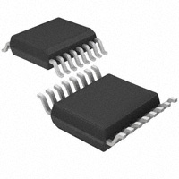
Available in a small TSSOP-16 Package
APPLICATIONS
D Digital Wireless Microphones
D Battery-Powered Audio Recording and
Processing Equipment
DESCRIPTION
The PCM4201 is designed for digital audio applications
that require a combination of high dynamic range, low
distortion, and low power consumption. The primary
applications for the PCM4201 include digital wireless
microphones and battery-operated audio recording or
processing equipment. The PCM4201 outputs 24-bit
linear PCM audio data at sampling rates up to 108kHz.
Three sampling modes allow the user to trade off power for
performance, dependent upon the intended system
requirements. An on-chip voltage reference reduces the
number of external components needed for operation.
The PCM4201 includes dedicated control pins for
configuration of all programmable functions. The device
requires a +5.0V analog power supply, in addition to a
digital supply operating from +1.8V to +3.3V. The
PCM4201 is available in a small TSSOP-16 package.
Please be aware that an important notice concerning availability, standard warranty, and use in critical applications of Texas Instruments
semiconductor products and disclaimers thereto appears at the end of this data sheet.
I2S is a registered trademark of Royal Philips Electronics B.V., The Netherlands. All other trademarks are the property of their respective owners.
Copyright 2004−2006, Texas Instruments Incorporated
��
���
�
��� ����������� �� ������� �� �� ����������� ����! ��������
������� �� �������������� ��� �"� ����� �� ��#��
���������� �������� $������%!
���������� ���������& ���� ��� ����������% ������� ������& �� ��� ����������!
www.ti.com
��������
www.ti.com
SBAS342B − DECEMBER 2004 − REVISED APRIL 2006
This integrated circuit can be damaged by ESD. Texas Instruments recommends that all integrated circuits be handled with appropriate
precautions. Failure to observe proper handling and installation procedures can cause damage.
ESD damage can range from subtle performance degradation to complete device failure. Precision integrated circuits may be more susceptible to
damage because very small parametric changes could cause the device not to meet its published specifications.
ABSOLUTE MAXIMUM RATINGS
over operating free-air temperature range unless otherwise noted(1)
PCM4201
UNIT
VCC
VDD
+6.0
V
Supply voltage
+3.6
V
Ground voltage differences
AGND to DGND
±0.1
V
Digital input voltage
RATE, S/M, RST, HPFD SCKI, BCK, FSYNC
−0.3 to (VDD + 0.3)
V
Analog input voltage
VIN+, VIN−
−0.3 to (VCC + 0.3)
V
±10mA
mA
−10 to +70
°C
Input current (any pin except supplies)
Operating temperature range
Storage temperature range, TSTG
−65 to +150
°C
(1) Stresses above those listed under Absolute Maximum Ratings may cause permanent damage to the device. Exposure to absolute maximum
conditions for extended periods may degrade device reliability. These are stress ratings only, and functional operation of the device at these or
any other conditions beyond those specified is not implied.
PACKAGE/ORDERING INFORMATION
For the most current package and ordering information, see the Package Option Addendum located at the end of this
datasheet, or see the TI website at www.ti.com.
2
��������
www.ti.com
SBAS342B − DECEMBER 2004 − REVISED APRIL 2006
ELECTRICAL CHARACTERISTICS
Unless otherwise specified, all characteristics are measured with TA = +25°C, VCC = +5V, and VDD = +3.3V. System clock frequency is set to
24.576 MHz. Device is operated in Slave mode.
PCM4201
PARAMETER
CONDITIONS
MIN
RESOLUTION
TYP
MAX
24
UNITS
Bits
AUDIO DATA FORMAT
Format
Two’s complement, MSB first data
Left-Justified / DSP Compatible
Word length
24
Bits
DIGITAL I/O
Input logic level
Output logic level
Input current
Input current(1)
VIH
VIL
0.7 x VDD
VDD
V
0
0.3 x VDD
V
VOH
IOH = −2mA
0.8 x VDD
VOL
IOL = +2mA
0.2 x VDD
V
V
IIH
VIN = VDD
+10
µA
IIL
VIN = 0V
−10
µA
IIH
VIN = VDD
+25
µA
IIL
VIN = 0V
−25
µA
54
kHz
DIGITAL SWITCHING
Normal speed, low power
Output sampling frequency
fS
8
Normal speed, high performance
8
54
kHz
Double speed
54
108
kHz
System clock duty cycle
45
System clock frequency
2.048
50
55
%
27.65
MHz
AUDIO SERIAL-PORT TIMING
Delay from FSYNC rising to BCK rising
tDBK
5
ns
Delay from BCK rising to FSYNC rising
tDLK
5
ns
BCK high pulse width
tBCKH
72
ns
BCK low pulse width
tBCKL
72
ns
Data setup time
tS
10
ns
Data hold time
tH
10
ns
ANALOG INPUTS
Input voltage, full-scale range (FSR)
Input impedance
Differential input
5.0
VPP
Per analog input pin
15
kΩ
100
dB
±4
% of FSR
±4
% of FSR
Common-mode rejection
DC PERFORMANCE
Output offset error
Gain error
High-pass filter disabled
(1) Applies to RATE (pin 5) and S/M (pin 6) inputs.
(2) All typical dynamic performance specifications were measured using an Audio Precision System Two Cascade or Cascade Plus test system and a PCM4201EVM
evaluation module. For Normal Speed operation, the measurement bandwidth is limited using the Audio Precision 22Hz high-pass filter and 20kHz low-pass filter.
For Double Speed mode, the measurement bandwidth is limited using the Audio Precision 22Hz high-pass filter and a user-defined 40kHz low-pass filter (the
fS/2 low pass filter may be utilized with similar results). All A-weighted measurements are made using the Audio Precision A-weighting filter in combination with
the filters previously noted here. Minimum and maximum dynamic performance limits are based upon the capability of the production test solution.
3
��������
www.ti.com
SBAS342B − DECEMBER 2004 − REVISED APRIL 2006
ELECTRICAL CHARACTERISTICS (continued)
Unless otherwise specified, all characteristics are measured with TA = +25°C, VCC = +5V, and VDD = +3.3V. System clock frequency is set to
24.576 MHz. Device is operated in Slave mode.
PCM4201
PARAMETER
CONDITIONS
MIN
TYP
MAX
UNITS
−103
−100
dB
DYNAMIC PERFORMANCE(2) with VCC = +5V and VDD = +1.8V
Normal Speed, Low Power, fS = 48kHz, BW = 22Hz to 20kHz
Total harmonic distortion + noise
THD+N
Dynamic range
VIN = −0.5dB, fIN = 1kHz
VIN = −60dB, fIN = 1kHz, A-weighted
Dynamic range, no weighting
104
VIN = −60dB, fIN = 1kHz
109
dB
106
dB
Normal Speed, High Performance, fS = 48kHz, BW = 22Hz to 20kHz
Total harmonic distortion + noise
THD+N
Dynamic range
VIN = −0.5dB, fIN = 1kHz
VIN = −60dB, fIN = 1kHz, A-weighted
Dynamic range, no weighting
−105
105
VIN = −60dB, fIN = 1kHz
−100
dB
112
dB
110
dB
Double Speed, fS = 96kHz, BW = 22Hz to 40kHz
Total harmonic distortion + noise
THD+N
Dynamic range
VIN = −0.5dB, fIN = 1kHz
VIN = −60dB, fIN = 1kHz, A-weighted
Dynamic range, no weighting
−103
105
VIN = −60dB, fIN = 1kHz
−100
dB
112
dB
106
dB
DYNAMIC PERFORMANCE(2) with VCC = +5V and VDD = +3.3V
Normal Speed, Low Power, fS = 48kHz, BW = 22Hz to 20kHz
Total harmonic distortion + noise
THD+N
Dynamic range
VIN = −0.5dB, fIN = 1kHz
VIN = −60dB, fIN = 1kHz, A-weighted
Dynamic range, no weighting
−102
104
VIN = −60dB, fIN = 1kHz
−100
dB
106
dB
104
dB
Normal Speed, High Performance, fS = 48kHz, BW = 22Hz to 20kHz
Total harmonic distortion + noise
THD+N
Dynamic range
VIN = −0.5dB, fIN = 1kHz
VIN = −60dB, fIN = 1kHz, A-weighted
Dynamic range, no weighting
−105
105
−100
dB
112
dB
VIN = −60dB, fIN = 1kHz
109
dB
VIN = −0.5dB, fIN = 1kHz
−103
Double Speed, fS = 96kHz, BW = 22Hz to 40kHz
Total harmonic distortion + noise
Dynamic range
Dynamic range, no weighting
THD+N
VIN = −60dB, fIN = 1kHz, A-weighted
105
VIN = −60dB, fIN = 1kHz
−100
dB
111
dB
106
dB
DIGITAL DECIMATION FILTER
Passband edge
0.453fS
Hz
Passband ripple
±0.005
dB
Stop band edge
Stop band attenuation
Group delay
0.547fS
Hz
−100
dB
37/fS
sec
(1) Applies to RATE (pin 5) and S/M (pin 6) inputs.
(2) All typical dynamic performance specifications were measured using an Audio Precision System Two Cascade or Cascade Plus test system and a PCM4201EVM
evaluation module. For Normal Speed operation, the measurement bandwidth is limited using the Audio Precision 22Hz high-pass filter and 20kHz low-pass filter.
For Double Speed mode, the measurement bandwidth is limited using the Audio Precision 22Hz high-pass filter and a user-defined 40kHz low-pass filter (the
fS/2 low pass filter may be utilized with similar results). All A-weighted measurements are made using the Audio Precision A-weighting filter in combination with
the filters previously noted here. Minimum and maximum dynamic performance limits are based upon the capability of the production test solution.
4
��������
www.ti.com
SBAS342B − DECEMBER 2004 − REVISED APRIL 2006
ELECTRICAL CHARACTERISTICS (continued)
Unless otherwise specified, all characteristics are measured with TA = +25°C, VCC = +5V, and VDD = +3.3V. System clock frequency is set to
24.576 MHz. Device is operated in Slave mode.
PCM4201
PARAMETER
CONDITIONS
MIN
TYP
MAX
UNITS
DIGITAL HIGH PASS FILTER
Frequency response (−3dB)
fS/48000
Hz
POWER SUPPLY
Supply voltage range
VCC
VDD
ICC
Operating supply current
with VCC = +5V, VDD = +1.8V
IDD
ICC
Operating supply current
with VCC = +5V, VDD = +3.3V
IDD
Power-Down mode current
with VCC = +5V, VDD = +1.8V or +3.3V
Total power dissipation
with VCC = +5V, VDD = +3.3V
Total power dissipation
with VCC = +5V, VDD = +1.8V
+4.75
+5.0
+5.25
+1.65
V
+3.3
+3.6
V
Normal speed, low power
7
8.2
mA
Normal speed, high performance
13
15
mA
Double speed
13
16
mA
Normal speed, low power
2
3.2
mA
Normal speed, high performance
2.5
4.5
mA
Double speed
3.5
6.0
mA
Normal speed, low power
7
8.2
mA
Normal speed, high performance
13
15
mA
Double speed
13
16
mA
Normal speed, low power
4
6.0
mA
Normal speed, high performance
5
8.5
mA
Double speed
7.5
10.5
mA
5
µA
ICC
5
µA
Normal speed, low power
49
61
mW
Normal speed, high performance
82
103
mW
IDD
Double speed
90
115
mW
Normal speed, low power
39
47
mW
Normal speed, high performance
70
83
mW
Double speed
72
91
mW
(1) Applies to RATE (pin 5) and S/M (pin 6) inputs.
(2) All typical dynamic performance specifications were measured using an Audio Precision System Two Cascade or Cascade Plus test system and a PCM4201EVM
evaluation module. For Normal Speed operation, the measurement bandwidth is limited using the Audio Precision 22Hz high-pass filter and 20kHz low-pass filter.
For Double Speed mode, the measurement bandwidth is limited using the Audio Precision 22Hz high-pass filter and a user-defined 40kHz low-pass filter (the
fS/2 low pass filter may be utilized with similar results). All A-weighted measurements are made using the Audio Precision A-weighting filter in combination with
the filters previously noted here. Minimum and maximum dynamic performance limits are based upon the capability of the production test solution.
5
��������
www.ti.com
SBAS342B − DECEMBER 2004 − REVISED APRIL 2006
PIN ASSIGNMENT
PW PACKAGE
TSSOP-16
(TOP VIEW)
VIN+
1
16
VREF+
VIN−
2
15
VREF−
AGND
3
14
DGND
VCC
4
13
VDD
RATE
5
12
SCKI
S/M
6
11
BCK
RST
7
10
FSYNC
HPFD
8
9
PCM4201
DATA
Terminal Functions
TERMINAL
PIN NO.
NAME
I/O
Input
Noninverting Analog Input
2
VIN+
VIN−
Input
Inverting Analog Input
3
AGND
Ground
Analog Ground
4
VCC
Power
Analog Supply, +5V
5
RATE
Input
Sampling Mode Configuration (Tri-Level Input): 0 = Double Speed;
1 = Normal Speed, Low Power; Z = Normal Speed, High Performance.
Maximum external capacitive load is 100pF.
6
S/M
Input
Audio Serial Port Slave/Master Mode (0 = Master, 1 = Slave)
7
RST
Input
Reset/Power Down (Active Low)
8
HPFD
Input
High Pass Filter Disable (Active High)
9
DATA
Output
10
FSYNC
I/O
Audio Serial Port Frame Synchronization Clock
11
BCK
I/O
Audio Serial Port Bit (or Data) Clock
12
SCKI
Input
13
VDD
Power
Digital Supply, +3.3V Typical(1)
14
DGND
Ground
Digital Ground
15
VREF−
Output
Voltage Reference Low Output, Connect to AGND
1
DESCRIPTION
Audio Serial Port Data
System Clock
16
VREF+
Output
Voltage Reference High Output, De-Coupling Only(2)
(1) The VDD supply may be operated from +1.8V to +3.6V.
(2) Unbuffered output. Do not use to drive external circuitry.
6
��������
www.ti.com
SBAS342B − DECEMBER 2004 − REVISED APRIL 2006
TYPICAL CHARACTERISTICS
At TA = 25°C, VDD = 1.8V, VCC = 5.0V, Master Mode, SCKI = 24.576MHz, unless otherwise noted.
HIGH−PERFORMANCE FFT PLOT
(fS = 48kHz, fIN = 997Hz at −1dB)
0
−20
−20
−40
−40
Amplitude (dB)
Amplitude (dB)
0
−60
−80
−100
−80
−100
−120
−140
−140
−160
20
100
1k
Frequency (Hz)
10k
20
24k
HIGH−PERFORMANCE FFT PLOT
(f S = 48kHz, fIN = 997Hz at −60dB)
0
−20
−20
−40
−40
−60
−80
−100
100
1k
Frequency (Hz)
10k
24k
10k
24k
10k
24k
LOW−POWER FFT PLOT
(fS = 48kHz, fIN = 997Hz at −1dB)
0
Amplitude (dB)
Amplitude (dB)
−60
−120
−160
−60
−80
−100
−120
−120
−140
−140
−160
−160
20
100
1k
Frequency (Hz)
10k
24k
20
LOW−POWER FFT PLOT
(f S = 48kHz, fIN = 997Hz at −20dB)
0
−20
−40
−40
−60
−80
−100
100
1k
Frequency (Hz)
LOW−POWER FFT PLOT
(f S = 48kHz, fIN = 997Hz at −60dB)
0
−20
Amplitude (dB)
Amplitude (dB)
HIGH−PERFORMANCE FFT PLOT
(fS = 48kHz, fIN = 997Hz at −20dB)
−60
−80
−100
−120
−120
−140
−140
−160
−160
20
100
1k
Frequency (Hz)
10k
24k
20
100
1k
Frequency (Hz)
7
��������
www.ti.com
SBAS342B − DECEMBER 2004 − REVISED APRIL 2006
TYPICAL CHARACTERISTICS (continued)
At TA = 25°C, VDD = 1.8V, VCC = 5.0V, Master Mode, SCKI = 24.576MHz, unless otherwise noted.
DOUBLE−SPEED FFT PLOT
(fS = 96kHz, fIN = 997Hz at −1dB)
0
−20
−20
−40
−40
Amplitude (dB)
Amplitude (dB)
0
−60
−80
−100
−100
−140
−140
−160
100
1k
Frequency (Hz)
10k
48k
20
DOUBLE−SPEED FFT PLOT
(f S = 96kHz, fIN = 997Hz at −60dB)
0
−100
100
1k
Frequency (Hz)
10k
48k
THD+N vs AMPLITUDE, HIGH PERFORMANCE
(fS = 48kHz, fIN = 997Hz, BW = 20Hz to 20kHz)
−102
−20
−104
−40
−106
−60
THD+N (dB)
Amplitude (dB)
−80
−120
20
−80
−100
VDD = 3.3V
−108
−110
−112
VDD = 1.8V
−114
−120
−116
−140
−118
−160
−120
20
−100
100
1k
Frequency (Hz)
10k
−120
48k
THD+N vs AMPLITUDE, LOW POWER
(fS = 48kHz, f IN = 997Hz, BW = 20Hz to 20kHz)
−100
VDD = 3.3V
−102
−104
−106
−106
−108
VDD = 1.8V
−110
−112
−116
−118
−118
−120
−120
−60
−40
Amplitude (dB)
−20
0
−20
0
VDD = 3.3V
VDD = 1.8V
−112
−114
−80
−60
−40
Amplitude (dB)
THD+N vs AMPLITUDE, DOUBLE SPEED
(fS = 96kHz, f IN = 997Hz, BW = 20Hz to 40kHz)
−110
−116
−100
−80
−108
−114
−120
−100
−102
−104
THD+N (dB)
THD+N (dB)
−60
−120
−160
8
DOUBLE−SPEED FFT PLOT
(fS = 96kHz, fIN = 997Hz at −20dB)
−120
−100
−80
−60
−40
Amplitude (dB)
−20
0
��������
www.ti.com
SBAS342B − DECEMBER 2004 − REVISED APRIL 2006
TYPICAL CHARACTERISTICS (continued)
At TA = 25°C, VDD = 1.8V, VCC = 5.0V, Master Mode, SCKI = 24.576MHz, unless otherwise noted.
THD+N vs FREQUENCY, HIGH PERFORMANCE
(fS = 48kHz, Input Level = −1dB, BW = 20Hz to 20kHz)
−90.0
−92.5
−92.5
−95.0
−97.5
−95.0
−97.5
VDD = 3.3V
THD+N (dB)
−100.0
−102.5
−105.0
−107.5
−110.0
VDD = 1.8V
−112.5
−105.0
−107.5
−110.0
−115.0
−117.5
−120.0
100
VDD = 1.8V
−112.5
−117.5
−120.0
20
VDD = 3.3V
−100.0
−102.5
−115.0
1k
Frequency (Hz)
10k
20k
20
100
1k
Frequency (Hz)
10k
20k
THD+N vs FREQUENCY, DOUBLE SPEED
(fS = 96kHz, Input Level = −1dB, BW = 20Hz to 40kHz)
−90.0
−92.5
−95.0
−97.5
THD+N (dB)
THD+N (dB)
−90.0
THD+N vs FREQUENCY, LOW POWER
(fS = 48kHz, Input Level = −1dB, BW = 20Hz to 20kHz)
VDD = 3.3V
−100.0
−102.5
−105.0
−107.5
−110.0
VDD = 1.8V
−112.5
−115.0
−117.5
−120.0
20
100
1k
Frequency (Hz)
10k
40k
9
��������
www.ti.com
SBAS342B − DECEMBER 2004 − REVISED APRIL 2006
PRODUCT OVERVIEW
The PCM4202 is a single channel audio analog-to-digital
converter (ADC) designed for use in low power, batteryoperated or portable professional audio equipment. Target
applications include digital wireless microphones and
portable digital audio recorders/processors. The
PCM4201 features 24-bit linear PCM output data, with a
format compatible with digital signal processors, digital
audio interface transmitters, and programmable logic
devices.
The PCM4201 includes three sampling modes, supporting
sampling rates up to 108kHz. The Normal Speed, Low
Power mode supports sampling rates up to 54kHz, and
employs 64x oversampling to reduce overall converter
power. The Normal Speed, High Performance mode
supports sampling rates up to 54kHz with 128x
oversampling, resulting in improved dynamic range and
THD+N when compared to the Low Power mode, at the
VINR+
VINR−
VREF+
VREF−
Delta−Sigma
Modulator
Decimation
Filter
expense of increased power dissipation. The Double
Speed mode supports sampling frequencies up to 108kHz
and is provided for those applications where higher
sampling rates may be required.
A digital high-pass filter is included for DC removal.
Dedicated control pins are included for sampling mode
selection, Slave/Master mode audio serial port operation,
digital high-pass filter enable/disable, and reset/
power-down functions.
A +5V power supply is required for the analog section of
the device, while a +3.3V power supply is typically utilized
for the digital section. The digital supply may be operated
at voltages as low as +1.8V, with a corresponding 10 to 20
milliwatt (mW) reduction in power dissipation, depending
upon the sampling mode selection. Figure 1 shows the
functional block diagram for the PCM4201.
HPF
FSYNC
Audio
Serial
Port
Voltage
Reference
BCK
DATA
S/M
HPFD
Reset
Logic
Power
Clock
Control
RATE
SCKI
RST
VCC
AGND
VDD
DGND
Figure 1. PCM4201 Functional Block Diagram
10
��������
www.ti.com
SBAS342B − DECEMBER 2004 − REVISED APRIL 2006
ANALOG INPUTS
The PCM4201 features differential voltage inputs. VIN+
(pin 1) and VIN− (pin 2) provide the noninverting and
inverting inputs, respectively. The full-scale input voltage,
measured differentially across these two pins, is
approximately 5.0VPP. The input impedance is
approximately 15kΩ per input pin.
In applications where the analog inputs can be driven
beyond the analog supply rails of the PCM4201, the input
buffer circuit should incorporate clamping or limiting
circuitry to ensure that the analog inputs are not driven
beyond the absolute maximum input levels for these pins.
Refer to the Absolute Maximum Ratings table of this
datasheet.
VOLTAGE REFERENCE
The PCM4201 includes an on-chip band gap reference for
the delta-sigma modulator, eliminating the need for
external reference circuitry. The reference voltage is set to
+2.5V nominal. The VREF+ (pin 16) and VREF− (pin 15)
outputs provide connections for reference decoupling
capacitors, which are connected between these two pins.
The VREF− output is then connected to analog ground.
Figure 2 shows the recommended decoupling capacitor
connections and values.
PCM4201
VREF+
16
0.1µF
VREF−
+
10µF
SCKI (pin 12). The acceptable system clock frequency
and duty cycle range are listed in the Electrical
Characteristics table of this datasheet.
The PCM4201 supports specific system clock rates, which
are multiples of the desired output sampling frequency.
The supported system clock rate is also dependent upon
the audio serial port mode. Table 1 and Table 2 specify the
system clock rates required for common output sampling
frequencies for both Slave and Master mode audio
serial-port operation.
Table 1. System Clock Rates for Common Audio
Sampling Frequencies—Slave Mode Operation
SYSTEM CLOCK
FREQUENCY (MHZ)
SAMPLING
MODE
SAMPLING
FREQUENCY
(kHz)
SCKI = 256fS
SCKI = 512fS
Normal
Normal
Normal
Double
Double
32
44.1
48
88.2
96
8.192
11.2896
12.288
22.5792
24.576
16.384
22.5792
24.576
N/A
N/A
Table 2. System Clock Rates for Common Audio
Sampling Frequencies—Master Mode Operation
SYSTEM CLOCK
FREQUENCY (MHZ)
SAMPLING
MODE
SAMPLING
FREQUENCY
(kHz)
SCKI = 256fS
SCKI = 512fS
Normal
Normal
Normal
Double
Double
32
44.1
48
88.2
96
N/A
N/A
N/A
22.5792
24.576
16.384
22.5792
24.576
N/A
N/A
15
AGND
Figure 2. Voltage Reference Connections
The voltage reference output is not buffered, and should
not be connected to external circuitry other than the
decoupling capacitors. DC common-mode voltage for the
input buffer circuitry may be set using an external voltage
divider circuit, as shown in the Applications Information
section of this datasheet.
SYSTEM CLOCK
The PCM4201 requires an external system clock, which is
used internally to derive the modulator oversampling and
digital subsystem clocks. The system clock is input at
SAMPLING MODES
The PCM4201 supports three sampling modes, allowing the
user to select the most appropriate power/performance
combination for a given application. The following
paragraphs describe the operation and tradeoffs for the three
sampling modes. For all cases, fS is defined as the desired
output sampling rate at the audio serial port interface.
Normal Speed, Low Power mode provides the lowest
overall power dissipation, while supporting sampling rates
up to 54kHz. The modulator oversampling rate is 64fS for
this mode, which results in lower dynamic range and
THD+N when compared to Normal Speed, High
Performance mode. For best dynamic performance and
lowest power consumption when using Low Power mode,
it is recommended to operate the PCM4201 from a +1.8V
digital power supply.
11
��������
www.ti.com
SBAS342B − DECEMBER 2004 − REVISED APRIL 2006
Normal Speed, High Performance mode provides the best
overall dynamic performance at the expense of increased
power dissipation. Sampling rates up to 54kHz are
supported. The modulator oversampling rate is 128fS for
this mode, improving the overall dynamic range and
THD+N when compared to Low Power mode.
Double Speed mode supports sampling frequencies up to
108kHz with power dissipation that is somewhat higher
than Normal Speed, High Performance mode. The
modulator oversampling rate is 64fS for this mode.
The sampling mode is selected using the RATE input (pin
5). The RATE pin is a tri-level logic input, with the ability to
detect low, high, and floating (or high-impedance) states.
Table 3 shows the available sampling mode
configurations using the RATE pin. For the floating or
high-impedance case, it is best to drive the RATE pin with
a tri-state buffer, such as the Texas Instruments
SN74LVC1G125 or equivalent. This allows the buffer to be
disabled, setting the output to a high-impedance state.
Table 3. Sampling Mode Configuration
RATE (PIN 5)
SAMPLING MODE SELECTION
0
1
Float or Hi Z
Double Speed
Normal Speed, Low Power
Normal Speed, High Performance
AUDIO SERIAL PORT
The PCM4201 audio serial port is a 3-wire synchronous
serial interface comprised of the audio serial data output,
DATA (pin 9); a frame synchronization clock, FSYNC (pin
10); and a bit or data clock, BCK (pin 11). The FSYNC and
BCK clocks may be either inputs or outputs, supporting
either Slave or Master mode interfaces, respectively. The
audio data format is 24-bit linear PCM, represented as
two’s complement binary data with the MSB being the first
data bit in the frame. Figure 3 illustrates the audio frame
format, while Figure 4 and the Electrical Characteristics
table highlight the important timing parameters for the
audio serial port interface.
One Frame (1)(2)
1/fS
FSYNC (3)
Slave Mode
Frame Format
DATA
Data (4)
FSYNC (5)
Master Mode
Frame Format
DATA
Data (4)
NOTES: (1) One Frame = 128 BCK clock cycles for Normal Speed modes and 64 BCK clock cycles for Double Speed mode.
(2) If BCK = 128f S when Normal Speed, Low Power sampling is enabled, then the frame will begin on the falling edge of the FSYNC clock input.
The FSYNC clock is inverted for this case.
(3) For Slave Mode operation, the FSYNC pulse width high period must be at least one BCK clock cycle in length, while the FSYNC pulse low
period must be at least one BCK clock cycle in length. Best performance is achieved when the FSYNC duty cycle is 50%.
(4) The audio data word length is 24 bits and is Left−Justified in the frame. The audio data is always presented in two’s complement binary format
with the MSB being the first data bit in the frame.
(5) For Master mode operation, the FSYNC clock duty cycle is equal to 50%.
Figure 3. Audio Serial-Port Frame Format
tDLK
FSYNC
tDBK
t BCKH
tBCKL
BCK
DATA
tS
tH
Figure 4. Audio Serial-Port Timing
12
��������
www.ti.com
SBAS342B − DECEMBER 2004 − REVISED APRIL 2006
Slave mode operation requires that the FSYNC and BCK
clocks be generated from an external audio processor or
master timing generator, as shown in Figure 5. Both clocks
are inputs in Slave mode. The FSYNC clock rate is the
equal to the desired output sampling frequency, fS. The
FSYNC high pulse width must be equal to at least one BCK
clock period. The BCK clock rate should be 128fS for
Normal Speed, High Performance sampling mode. A BCK
rate equal to 64fS results in no output for this sampling
mode. For Normal Speed, Low Power sampling mode, the
BCK rate may be 64fS or 128fS. See Note (2) in Figure 3
regarding the FSYNC edge used for start of frame when
BCK = 128fS for this sampling mode. For Double Speed
sampling mode, the BCK rate should be 64fS.
AUDIO DSP
PCM4201
FSR
FSYNC
CLKR
SCKI
DIGITAL HIGH-PASS FILTER
The PCM4201 includes a digital high-pass filter, which is
located at the output of the digital decimation filter block.
The purpose of the high-pass filter is to remove the DC
component from the digitized signal. The corner, or −3dB
frequency, for the digital high-pass filter is calculated using
the following relationship:
f *3dB +
fS
48000
(1)
where fS = the output sampling frequency.
The digital high-pass filter may be enabled or disabled
using the HPFD input (pin 8). When HPFD is forced low,
the high-pass filter is enabled. Forcing HPFD high
disables the high-pass filter. Distortion for signal
frequencies less than 100Hz may increase slightly when
the high-pass filter is enabled.
BCK
DR
RESET OPERATION
DATA
S/M
VDD
System
Clock
Figure 5. PCM4201 Slave Mode Configuration
For Master mode operation, the PCM4201 generates the
FSYNC and BCK clocks, deriving them from the system
clock input, SCKI (pin 12), as shown in Figure 6. The
FSYNC clock rate is equal to the output sampling
frequency, fS. The FSYNC clock duty cycle is 50% in
Master mode. The BCK clock rate is fixed at 128fS for
Normal Speed, High Performance sampling mode. For
Normal Speed, Low Power, and Double Speed sampling
modes, the BCK rate is fixed at 64fS.
AUDIO DSP
PCM4201
FSR
FSYNC
CLKR
SCKI
BCK
DR
DATA
S/M
DGND
System
Clock
The PCM4201 includes two reset functions: power-on and
externally controlled. This section describes the operation
of each of these functions.
On power up, the internal reset signal is forced low, forcing
the PCM4201 into a reset state. The power-on reset circuit
monitors the VDD (pin 13) and VCC (pin 4) power supplies.
When the digital supply exceeds 0.6 × VDD nominal
±400mV, and the VCC supply exceeds +4.0V ±400mV, the
internal reset signal is forced high. The PCM4201 will then
wait for the system clock input (SCKI) to become active.
Once the system clock has been detected, the initialization
sequence begins. The initialization sequence requires
1024 system clock periods for completion. During the
initialization sequence, the ADC output data pin will be
forced low. Once the initialization sequence is completed,
the PCM4201 outputs valid data. Figure 7 shows the
power-on reset sequence timing.
The user may force a reset initialization sequence at any
time while the system clock input is active by utilizing the
RST input (pin 7). The RST input is active low, and requires
a minimum low pulse width of 40ns. The low-to-high
transition of the applied reset signal will force an
initialization sequence to begin. As in the case of the
power-on reset, the initialization sequence requires 1024
system clock periods for completion. Figure 8 illustrates
the reset sequence initiated when using the RST input.
Figure 9 shows the state of the audio data output (DATA)
for the PCM4201 before, during, and after the reset
operations.
Figure 6. PCM4201 Master Mode Configuration
13
��������
www.ti.com
SBAS342B − DECEMBER 2004 − REVISED APRIL 2006
~ 4.0V
VCC
0V
0.6 x VDD
VDD
Internal
Reset
Nominal(1)
0V
1024 System Clock Periods
Required for Initialization
0V
SCKI
0V
System Clock
Indeterminate
or Inactive
(1) VDD nominal range is +1.8V to +3.6V.
Figure 7. Power-On Reset Sequence
tRSTL > 40ns
RST
0V
Internal
Reset
0V
1024 System Clock Periods
Required for Initialization
SCKI
0V
Figure 8. External Reset Sequence
Internal
Reset
HI
LO
Output
Data Pins
Valid Output Data
Outputs Forced Low
Outputs Forced Low
for 1024 SCKI Periods
Initialization
Period
Figure 9. ADC Digital Output State for Reset Operation
14
Valid Output Data
��������
www.ti.com
SBAS342B − DECEMBER 2004 − REVISED APRIL 2006
POWER-DOWN OPERATION
The PCM4201 can be forced to a power-down state by
applying a low level to the RST input (pin 7) for a minimum
of 65,536 system clock cycles. In power-down mode, all
internal clocks are stopped, and the output data pin is
forced low. The system clock may then be removed to
conserve additional power. Before exiting power-down
mode, the system and audio clocks should be restarted.
Once the clocks are active, the RST input may be driven
high, which initiates a reset initialization sequence.
Figure 10 illustrates the state of the output data pins
before, during, and upon exiting the power-down state.
HI
RST
LO
Output
Data Pins
Valid Output Data
Outputs
Forced Low
65,536
SCKI Periods
Outputs
Forced Low
Enter
Power−Down
State
Outputs
Forced Low
Valid Output Data
1024 SCKI Periods
Required for Initialization
Figure 10. ADC Digital Output State for Power-Down Operation
15
��������
www.ti.com
SBAS342B − DECEMBER 2004 − REVISED APRIL 2006
APPLICATIONS INFORMATION
A typical connection diagram for the PCM4201 is shown
in Figure 11. Power supply bypass and reference
decoupling capacitors are included, and are labeled with
recommended values. The 0.1µF capacitors should be
X7R ceramic chip type, although other low ESR capacitor
types may also be used. The 10µF capacitors may be low
ESR tantalum, multilayer ceramic, or aluminum
electrolytic capacitors. Analog and digital ground pins
should be connected at a common point, preferably
beneath the PCM4201 package.
Printed circuit board layout is critical for best performance.
Please refer to the PCM4201EVM User’s Guide (TI
literature number SBAU108) for an example of a design
and layout that meets the published specifications for the
PCM4201.
INPUT BUFFER CIRCUIT EXAMPLES
The PCM4201 analog input requires some type of input
buffer or signal conditioning circuitry, especially when
interfacing to a microphone capsule. The input buffer or
amplifier must incorporate at least a single pole, RC
low-pass filter in order to provide antialias filtering for the
delta-sigma modulator. A filter with a −3dB corner
frequency in the range of 100kHz to 150kHz should be
sufficient for common audio output sampling rates equal to
or greater than 44.1kHz. However, a low-pass filter with a
lower corner frequency and possibly a higher filter order
will be required when running at the lower sampling rates,
depending upon the system requirements. Examples of
single-ended and differential input circuits are shown in
Figure 12 and Figure 13, respectively.
Input
Buffer
1
Analog
Input
2
3
+
10µF
+5V
0.1µF 4
5
From
Control
Logic
6
7
8
VIN+
VREF+
VIN−
VREF−
AGND
DGND
VCC
VDD
PCM4201
RATE
SCKI
S/M
BCK
RST
FSYNC
HPFD
DATA
16
15
+
0.1µF
10µF
14
13
0.1µF
12
+
10µF
+1.8V to +3.6V
11
10
9
DSP, FPGA,
or
DIT4096
System Clock
Figure 11. Typical Connections for the PCM4201
16
��������
www.ti.com
SBAS342B − DECEMBER 2004 − REVISED APRIL 2006
For single-ended or unbalanced inputs, the input buffer
circuit shown in Figure 12 provides the conversion to a
differential signal required for the PCM4201 analog inputs.
The buffer circuit may be configured for the appropriate
gain/attenuation using resistors R1 and R2. Capacitor C1
is chosen to provide the low-pass corner frequency.
Additional low-pass filtering is provided by the RC network
at the output of the buffer.
A differential input buffer circuit is shown in Figure 13. Like
the unbalanced circuit, the differential buffer
gain/attenuation may be set by using the R1/R2 and R3/R4
resistor pairs. The resulting gain or attenuation must be the
same for both pairs. Filtering is provided by the feedback
capacitors and the capacitors at the buffer output. This
circuit configuration is used for the PCM4201EVM
evaluation module.
C1
R2
10µF
to 100µF
100pF
R1
40.2Ω
Analog
Input
VIN−
U1A
2.49kΩ
2.49kΩ
+5V
0.022µF
40.2Ω
10kΩ
VIN+
U1B
+
10kΩ
100pF
10µF
0.1µF
NOTE: U1 = OPA2134 or equivalent.
Figure 12. Single-Ended Input Buffer Circuit
R2
1000pF
10µF
to 100µF
R1
40.2Ω
VIN+
U1A
+5V
100pF
Analog
Input
10kΩ
2
0.1µF
1
2700pF
3
Ground
Lift
Switch
+
10µF
10µF
to 100µF
10kΩ
40.2Ω
R3
VIN−
U1B
100pF
1000pF
NOTE: U1 = OPA2134 or equivalent.
R4
Figure 13. Differential Input Buffer Circuit
17
��������
www.ti.com
SBAS342B − DECEMBER 2004 − REVISED APRIL 2006
INTERFACING TO THE DIT4096 DIGITAL AUDIO
TRANSMITTER
The Texas Instruments DIT4096 digital audio transmitter
encodes linear PCM audio data into AES3 standard
formatted data, which is compatible with a number of
professional and consumer audio specifications and
interfaces. This encoding provides a convenient, standard
transmission format over which the audio data from the
PCM4201 may be carried. The physical interface may be
twisted pair or coaxial cable, or all-plastic optical fiber. The
combination of the PCM4201, the DIT4096, and the
appropriate microphone element and preamplifier circuit
may be used to create a cost-effective, digital-interface
microphone solution.
Preamplifier/Buffer
Microphone
Capsule
The PCM4201 output data format is equivalent to the
Left-Justified data format supported by the DIT4096
transmitter. Although this format supports two channels for
stereo operation, the PCM4201 provides only one
channel, which corresponds to the left data channel of the
DIT4096 Left-Justified data format, and channel A of the
AES3 frame format. Figure 14 shows the physical
interface between the PCM4201 and the DIT4096
transmitter. The digital supply for the PCM4201 (VDD) and
the digital I/O supply for the DIT4096 (VIO) must be set to
the same voltage in order to ensure logic level
compatibility.
PCM4201
VIN+
DIT4096
BCK
SCLK
FSYNC
SYNC
TX+
VIN−
DATA
SDIN
TX−
S/M
SCKI
MCLK
M/S
Master
Clock
NOTES: The PCM4201 is in Master mode, while the DIT4096 is in Slave mode.
Both operate from the same Master clock source.
The data format for the DIT4096 is configured for Left−Justified mode.
Figure 14. Digital Interface Microphone Example
18
To
Balanced or Unbalanced
Line Interface or
Optical Transmitter
��������
www.ti.com
SBAS342B − DECEMBER 2004 − REVISED APRIL 2006
Revision History
DATE
REV
PAGE
SECTION
DESCRIPTION
Added new Note (2) to Figure 3.
12
4/12/06
Product Overview
Changed order of notes in Figure 3 to accommodate new Note (2).
Replaced last sentence of first paragraph, left column to clarify BCK rate.
Several sentences used to replace original sentence.
B
13
Product Overview
Changed last sentence of second paragraph, left column to clarify BCK rate.
Several sentences used to replace original sentence.
NOTE: Page numbers for previous revisions may differ from page numbers in the current version.
19
�PACKAGE OPTION ADDENDUM
www.ti.com
10-Dec-2020
PACKAGING INFORMATION
Orderable Device
Status
(1)
Package Type Package Pins Package
Drawing
Qty
Eco Plan
(2)
Lead finish/
Ball material
MSL Peak Temp
Op Temp (°C)
Device Marking
(3)
(4/5)
(6)
PCM4201PW
ACTIVE
TSSOP
PW
16
90
RoHS & Green
NIPDAU
Level-2-260C-1 YEAR
-10 to 70
PCM
4201
PCM4201PWR
ACTIVE
TSSOP
PW
16
2500
RoHS & Green
NIPDAU
Level-2-260C-1 YEAR
-10 to 70
PCM
4201
PCM4201PWRG4
ACTIVE
TSSOP
PW
16
2500
RoHS & Green
NIPDAU
Level-2-260C-1 YEAR
-10 to 70
PCM
4201
(1)
The marketing status values are defined as follows:
ACTIVE: Product device recommended for new designs.
LIFEBUY: TI has announced that the device will be discontinued, and a lifetime-buy period is in effect.
NRND: Not recommended for new designs. Device is in production to support existing customers, but TI does not recommend using this part in a new design.
PREVIEW: Device has been announced but is not in production. Samples may or may not be available.
OBSOLETE: TI has discontinued the production of the device.
(2)
RoHS: TI defines "RoHS" to mean semiconductor products that are compliant with the current EU RoHS requirements for all 10 RoHS substances, including the requirement that RoHS substance
do not exceed 0.1% by weight in homogeneous materials. Where designed to be soldered at high temperatures, "RoHS" products are suitable for use in specified lead-free processes. TI may
reference these types of products as "Pb-Free".
RoHS Exempt: TI defines "RoHS Exempt" to mean products that contain lead but are compliant with EU RoHS pursuant to a specific EU RoHS exemption.
Green: TI defines "Green" to mean the content of Chlorine (Cl) and Bromine (Br) based flame retardants meet JS709B low halogen requirements of


 工商网监
湘ICP备2023018690号
工商网监
湘ICP备2023018690号
