User's Guide
SBAU104A – August 2004 – Revised August 2014
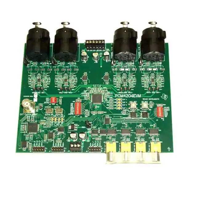
PCM4204EVM User's Guide
This document provides the information needed to set up and operate the PCM4204EVM evaluation
module (EVM). For a more detailed description of the PCM4204, please refer to the product datasheet
available from the Texas Instruments web site at http://www.ti.com. Additional support documents are
listed in the sections of this guide entitled Related Documentation from Texas Instruments and
Additional Documentation. Throughout this document, the acronym EVM and the phrase evaluation
module are synonymous with the PCM4204EVM. This user's guide includes setup and configuration
instructions, information regarding absolute operating conditions for power supplies and input/output
connections, an electrical schematic, PCB layout drawings, and a bill of materials (BOM) for the EVM.
1
2
3
4
Contents
Introduction ................................................................................................................... 3
Getting Started ............................................................................................................... 8
Hardware Description and Configuration ................................................................................. 9
Schematic, PCB Layout, and Bill of Materials .......................................................................... 16
List of Figures
1
PCM4204 Functional Block Diagram ...................................................................................... 4
2
PCM4204EVM Functional Block Diagram ................................................................................ 6
3
ADC Reset Circuitry........................................................................................................ 16
4
DIT (Transmitter) Reset Circuitry ......................................................................................... 16
5
PCM4204EVM Schematic-Analog Section
6
7
8
9
10
11
12
.............................................................................
PCM4204EVM Schematic-Digital Section ..............................................................................
Top Side Silkscreen ........................................................................................................
Bottom Side Silkscreen ....................................................................................................
Top Layer (Component Side) .............................................................................................
Ground Plane Layer........................................................................................................
Power Plane Layer .........................................................................................................
Bottom Layer (Solder Side) ...............................................................................................
17
18
20
21
22
23
24
25
List of Tables
1
Absolute Operating Conditions............................................................................................. 9
2
Audio Data Format Selection: Slave Mode Operation................................................................. 10
3
Audio Data Format Selection: Master Mode Operation ............................................................... 11
4
Sub-Frame Selection for TDM Data Formats........................................................................... 11
5
DSD-to-PCM Conversion Test Mode Selection ........................................................................ 11
6
System Clock Source Selection .......................................................................................... 12
7
Sampling Mode Selection: PCM Slave Mode Audio Formats ........................................................ 12
8
Sampling Mode Selection: PCM Master Mode Audio Formats
9
10
11
12
13
......................................................
Sampling Mode Selection: DSD Output Mode .........................................................................
Sampling Mode Selection: DSD Input Mode ...........................................................................
Digital High-Pass Filter Configuration ...................................................................................
Digital Interface Transmitter Configuration ..............................................................................
Transmitter Master Clock Configuration .................................................................................
SBAU104A – August 2004 – Revised August 2014
Submit Documentation Feedback
Copyright © 2004–2014, Texas Instruments Incorporated
PCM4204EVM User's Guide
12
13
13
13
14
14
1
�www.ti.com
2
14
Transmitter Audio Data Format Selection ............................................................................... 14
15
Mono Mode Configuration ................................................................................................. 15
16
PCM4204EVM Bill of Materials
PCM4204EVM User's Guide
..........................................................................................
26
SBAU104A – August 2004 – Revised August 2014
Submit Documentation Feedback
Copyright © 2004–2014, Texas Instruments Incorporated
�Introduction
www.ti.com
1
Introduction
The PCM4204 is a high-performance, four-channel audio analog-to-digital (A/D) converter designed for
use in professional and broadcast audio applications. The PCM4204 features simultaneous 24-bit linear
PCM or 1-bit Direct Stream Digital (DSD) data output for all four channels. Sampling rates up to 216kHz
are supported for PCM output formats, while 64x or 128x oversampled 1-bit data is supported for DSD
output and input modes. Native support for both PCM and DSD data formats makes the PCM4204 ideal
for use in a variety of audio recording and processing applications.
The PCM4204 features 1-bit delta-sigma (ΔΣ) modulators employing a novel density modulated dithering
scheme, yielding improved dynamic performance. Differential voltage inputs are utilized for the
modulators, providing excellent common-mode rejection. On-chip voltage references are provided for the
modulators, in addition to generating DC common-mode bias voltage outputs for use with external input
circuitry. Linear phase digital decimation filtering is provided for the 24-bit PCM output, with a minimum
stop band attenuation of -100dB for all sampling modes.
The PCM output mode features clipping flag outputs for each of the four channels, as well as a digital
high-pass filter for DC removal. The PCM4204 is configured using dedicated input pins for sampling mode
and audio data format selection, high-pass filter enable/disable, and reset/power-down operation.
A +5V power supply is required for the analog section of the device, while a +3.3V power supply is
required for the digital circuitry. Figure 1 shows the functional block diagram of the PCM4204.
SBAU104A – August 2004 – Revised August 2014
Submit Documentation Feedback
Copyright © 2004–2014, Texas Instruments Incorporated
PCM4204EVM User's Guide
3
�Introduction
VIN1+
VIN1−
www.ti.com
Delta−Sigma
Modulator
Digital
Decimation and High Pass
Filters
Audio
Serial
Port
LRCK
BCK
SDOUT1
SDOUT2
DSD
Data
Port
DSD1
DSD2
DSD3
DSD4
DSDCLK
VREF12+
VREF12−
AGND4
Reference
VCOM12
VIN2+
VIN2−
VIN3+
VIN3−
Control
and
Status
FS0
FS1
FS2
S/M
FMT0
FMT1
FMT2
HPFD
SUB
RST
CLIP1
CLIP2
CLIP3
CLIP4
System Clock
and
Timing
SCKI
Delta−Sigma
Modulator
Delta−Sigma
Modulator
To /From
Other Blocks
VREF34+
VREF34−
Reference
AGND3
VCOM34
To Other
Blocks
VIN4+
VIN4−
Delta−Sigma
Modulator
VCC1
AGND1
VCC2
AGND2
BGND1
BGND2
BGND3
BGND4
VDD1
DGND1
VDD2
DGND2
VDD3
DGND3
Power and Ground
Figure 1. PCM4204 Functional Block Diagram
4
PCM4204EVM User's Guide
SBAU104A – August 2004 – Revised August 2014
Submit Documentation Feedback
Copyright © 2004–2014, Texas Instruments Incorporated
�Introduction
www.ti.com
1.1
PCM4204EVM Features
The PCM4204EVM provides a convenient platform for evaluating the performance and functionality of the
PCM4204 product. The primary EVM features include:
• Simple configuration using onboard DIP switches
• Four differential voltage inputs supporting either 3-pin XLR or Balanced TRS connections
• Low-noise input buffer circuits utilizing the OPA1632 fully differential audio amplifier
• Four 75Ω AES3-encoded outputs, supporting operation up to 216kHz sampling rates
• Buffered Audio Serial Port supports a four-channel, 24-bit linear PCM data interface for external
hardware and signal processors. Sampling rates up to 216kHz are supported.
• DSD Data Port supports a four-channel, 1-bit output or input data interface at 64x or 128x data rates
• A second PCM4204 provides a test mode for 1-bit DSD to 24-bit linear PCM format conversions
• Two onboard system clock oscillators, operating at 22.5792MHz and 24.576MHz respectively,
supporting standard PCM sampling rates, including 44.1kHz, 48kHz, 88.2kHz, 96kHz, 176.4kHz, and
192kHz.
• External system clock inputs supporting alternative sampling rates up to 216kHz.
The PCM4204EVM requires +15V, -15V, and +5V analog power supplies. Additionally, a +5V digital
power supply is required, with a +3.3V digital supply being derived onboard using a linear voltage
regulator IC.
SBAU104A – August 2004 – Revised August 2014
Submit Documentation Feedback
Copyright © 2004–2014, Texas Instruments Incorporated
PCM4204EVM User's Guide
5
�Introduction
1.2
www.ti.com
PCM4204EVM General Description and Functional Block Diagram
J14
−15V
+15V
JMP6
+3.3VD
J5
GND
+5VD
+5VA
GND
−15
GND
GND
+15
The PCM4204EVM provides a complete platform for evaluating the performance and features of the
PCM4204 four-channel audio A/D converter. Figure 2 illustrates the functional block diagram for the
evaluation module.
BUF
U18
DIT4192
J9
AES3 Out #1
Stereo: Ch 1 + 2
Mono: Ch 1
DIT
U19
DIT4192
J10
AES3 Out #2
Stereo: Ch 1 + 2
Mono: Ch 2
U20
DIT4192
J11
AES3 Out #3
Stereo: Ch 3 + 4
Mono: Ch 3
U21
DIT4192
J12
AES3 Out #4
Stereo: Ch 3 + 4
Mono: Ch 4
To
DIT Circuitry
+5VA
+5VD
U23
REG1117
+3.3V
Switch
SW3
+3.3V
Switch
SW1
Analog
Input Buffers
OPA1632 x 4
J1
Channel 1
Input
BUF
HDR
J6
Audio
Serial Port
HDR
J7
DSD
Data Port
PCM Data
J2
Channel 2
Input
U1
PCM4204
J3
Channel 3
Input
S/M
FMT2
DSD Data
BUF
J4
Channel 4
Input
System
Clock
DSD Data
J13
EXT CLOCK INPUT
To
Clock Enables
Bus
Switch
DSDTEST
U2
PCM4204
PCM Data
Switch
SW5
X1
22.5792M
BUF
X2
24.576M
HDR
J8
DSD−to−PCM
Output Port
Figure 2. PCM4204EVM Functional Block Diagram
6
PCM4204EVM User's Guide
SBAU104A – August 2004 – Revised August 2014
Submit Documentation Feedback
Copyright © 2004–2014, Texas Instruments Incorporated
�Introduction
www.ti.com
Four differential analog inputs are supported at connectors J1 through J4, corresponding to analog input
channels 1 through 4, respectively. These connectors support either 3-pin male XLR or balanced TRS
input plugs. Each of the analog inputs is buffered and filtered using a low noise input circuit, utilizing a
Texas Instruments OPA1632 fully differential amplifier. The output of each buffer circuit is connected to a
corresponding differential input of the PCM4204 (U1). The PCM4204 is then used to convert the analog
signal to either a 24-bit linear PCM or 1-bit DSD representation in the digital domain.
The 24-bit PCM data output is made available at header J6, or at the AES3-encoded data outputs
provided at jacks J9 through J12. The buffered header is convenient for interfacing to external
development hardware or digital signal processors, while the AES3-encoded outputs may be connected to
audio test systems or commercial audio equipment.
The 1-bit DSD data is available at header J7. This header is bi-directional, and may be used for either
DSD output or input mode operation. A second PCM4204 (U2) is included for supporting a DSD-to-PCM
format conversion test or demo mode. The resulting PCM-formatted output data is made available at
header J8.
Power is connected to the board at either terminal block J5 for the analog supplies, or at terminal block
J14 for the digital supplies.
Manual reset circuits are provided for both the PCM4204 (U1 and U2) and the AES3 transmitters (U18
through U21). The ADC RESET switch (SW2) is utilized for resetting the A/D converters (U1 and U2),
while the DIT RESET switch (SW4) is utilized for resetting the AES3 transmitters (U18 through U21).
The system or master clock for the evaluation module may be generated onboard or by an external clock
source. Oscillators X1 and X2 operate at fixed clock frequencies of 22.5792MHz and 24.576MHz,
respectively. The oscillators provide low jitter clock sources for measuring the performance of the
PCM4204 in Master mode operation. Alternatively, an external clock source may be connected at J13 for
Master mode operation, supporting alternate system clock and sampling frequencies. For Slave mode
operation, the system clock is provided from an external source through header J6 and buffer U12. Switch
SW5 provides clock configuration control for the oscillators and the external clock input at connector J13.
1.3
Related Documentation from Texas Instruments
The following documents provide information regarding Texas Instrument integrated circuits used in the
assembly of the PCM4204EVM. The latest revisions of these documents are available from the TI web
site at http://www.ti.com.
Data Sheet
PCM4204 Datasheet
DIT4192 Datasheet
OPA227 Datasheet
OPA1632 Datasheet
REG1117 Datasheet
SN74AHC08 Datasheet
SN74AHC14 Datasheet
SN74ALVC245 Datasheet
SN74CBTLV3245A Datasheet
SN74LVC1G125 Datasheet
Literature Number
SBAS327
SBOS229
SBOS110
SBOS286
SBVS001
SCLS236
SCLS238
SCES271
SCDS034
SCES223
SBAU104A – August 2004 – Revised August 2014
Submit Documentation Feedback
Copyright © 2004–2014, Texas Instruments Incorporated
PCM4204EVM User's Guide
7
�Introduction
1.4
www.ti.com
Additional Documentation
The following documents or references provide information regarding selected non-TI components used in
the assembly of the PCM4204EVM. These documents are available from the corresponding manufacturer.
Document/Reference
SM7745H Series CMOS Oscillators
2
Manufacturer
Pletronics ( http://www.pletronics.com)
Getting Started
This section provides information regarding handling and unpacking the PCM4204EVM, as well as
absolute operating conditions for the unit.
2.1
Electrostatic Discharge Warning
CAUTION
Failure to observe proper ESD handling precautions may result in damage to
EVM components.
Many of the components on the PCM4204EVM are susceptible to damage by electrostatic discharge
(ESD). Customers are advised to observe proper ESD handling procedure when unpacking and handling
the EVM, including the use of a grounded wrist strap at an approved ESD workstation. Failure to observe
ESD handling procedures may result in damage to EVM components.
2.2
EVM Package Contents
Upon opening the PCM4204EVM package, please check to make sure that the following items are
included:
• One PCM4204EVM
• One printed copy of the PCM4204 product datasheet
• One printed copy of this PCM4204EVM User's Guide
If any of these items are missing, please contact the Texas Instruments Product Information Center
nearest you to inquire about replacements.
8
PCM4204EVM User's Guide
SBAU104A – August 2004 – Revised August 2014
Submit Documentation Feedback
Copyright © 2004–2014, Texas Instruments Incorporated
�Getting Started
www.ti.com
2.3
Absolute Operating Conditions
CAUTION
Exceeding the absolute operating conditions may result in damage to the
evaluation module and/or the equipment connected to it.
The user should be aware of the absolute operating conditions for the PCM4204EVM. Table 1
summarizes the critical data points.
Table 1. Absolute Operating Conditions
Min
Max
Units
+15V
+5.0
+16.0
V
-15V
-5.0
-16.0
V
+5VA
+4.5
+5.5
V
+5VD
+4.5
+5.5
V
EXT +3.3V
+3.0
+3.6
V
VIH, Input High Voltage (VDD = +3.0V to +3.6V)
0.7 x VDD
V DD + 0.3
V
VIL, Input Low Voltage (VDD = +3.0V to +3.6V)
-0.3
0.3 x VDD
V
Differential Input Voltage, RMS
7.9
V RMS
Differential Input Voltage, Peak-to-Peak
22.3
V PP
Power Supplies
Audio Serial Port (J6), DSD Data Port (J7)
Analog Inputs (connectors J1 and J2)
3
Hardware Description and Configuration
This section provides hardware description and configuration information for the PCM4204EVM.
3.1
Power Supply Configuration
The PCM4204EVM requires three analog power supplies and one digital power supply for operation. The
analog supplies are connected at terminal block J5, while the digital supply is connected at terminal block
J14.
Analog supplies include +15V and -15V DC for powering the input buffer circuits, as well as +5.0V DC for
powering the analog section of the PCM4204. All supplies should be rated for at least 500mA of output
current.
SBAU104A – August 2004 – Revised August 2014
Submit Documentation Feedback
Copyright © 2004–2014, Texas Instruments Incorporated
PCM4204EVM User's Guide
9
�Hardware Description and Configuration
www.ti.com
The digital supply requires +5.0V DC and should be rated for at least 500mA of output current. The +5.0V
supply is regulated to +3.3V DC by an onboard Texas Instruments REG1117 linear voltage regulator
(U23), which is used to power the digital section of the PCM4204 and the majority of the support logic
circuitry. The core logic and line driver sections of the AES3 transmitters (U18 through U21) utilize the
+5.0V digital supply directly.
An optional external +3.3V DC digital power supply is supported at terminal block J14. Jumper JMP6 is
utilized to select either the onboard voltage regulator (U23) or an external +3.3V power source. Shorting
pins 1 and 2 together using the supplied jumper block selects the onboard +3.3V voltage regulator.
Shorting pins 3 and 4 together will select the external +3.3V supply terminal (EXT +3.3VD) on terminal
block J14. Only one source may be selected at any time.
3.2
Analog Inputs
The PCM4204EVM includes four Neutrik combo XLR connectors, which accept either 3-pin male XLR or
¼-inch TRS phono plugs. The connectors are numbered J1 through J4, corresponding to Channels 1
through 4, respectively.
The analog inputs can accept up to a 7.9VRMS (or 22.3VPP) differential input signal. This signal is then
attenuated by a factor of 3.7 by the input buffer circuit, which corresponds to the 6.0VPP full-scale
differential input voltage for the PCM4204 analog inputs.
The input buffer circuits are each comprised of a single OPA1632 fully differential audio amplifier and
associated passive components. The input buffer provides active attenuation and low pass filtering for the
analog input signal. The OPA1632 outputs are DC level-shifted by approximately +2.5V using the
amplifiers VCOMIN input (pin 2), which are connected to a buffered version of either the PCM4204 VCOM12
(pin 61) or VCOM34 outputs (pin 52).
3.3
Audio Data Format Selection
Switch SW1 is used to select the audio data format for the PCM4204 (U1). Table 2 and Table 3
summarize the available audio data formats for both Slave and Master mode operation and the
corresponding SW1 switch settings.
Table 2. Audio Data Format Selection: Slave Mode Operation
10
S/M
FMT2
FMT1
FMT0
Audio Data Format
HI
LO
LO
LO
24-Bit Left Justified
HI
LO
LO
HI
24-Bit I2S
HI
LO
HI
LO
24-Bit Right Justified
HI
LO
HI
HI
TDM with No BCK Delay for Start of Frame
HI
HI
LO
LO
TDM with One BCK Delay for Start of Frame
HI
HI
LO
HI
Reserved
HI
HI
HI
LO
Reserved
HI
HI
HI
HI
Reserved
PCM4204EVM User's Guide
SBAU104A – August 2004 – Revised August 2014
Submit Documentation Feedback
Copyright © 2004–2014, Texas Instruments Incorporated
�Hardware Description and Configuration
www.ti.com
Table 3. Audio Data Format Selection: Master Mode Operation
S/M
FMT2
FMT1
FMT0
Audio Data Format
LO
LO
LO
LO
24-Bit Left Justified
LO
LO
LO
HI
24-Bit I2S
LO
LO
HI
LO
24-Bit Right Justified
LO
LO
HI
HI
DSD Output with PCM Output Disabled
LO
HI
LO
LO
DSD Input with 24-Bit Right Justified PCM Output
LO
HI
LO
HI
Reserved
LO
HI
HI
LO
Reserved
LO
HI
HI
HI
Reserved
For Slave mode operation, the Audio Serial Port header (connector J6) is utilized to interface to a Master
device, such as a digital signal processor, FPGA, or an audio test system with a synchronous serial port
interface. The system clock (SCKI), bit clock (BCK), and left/right word clock (LRCK) are generated by the
Master device and are used to drive the SCKI (pin 15), BCK (pin 29), and LRCK (pin 30) inputs of the
PCM4204. Serial audio data is output at SDOUT1 (pin 31) and SDOUT2 (pin 32). Slave mode supports
PCM-formatted output data only. DSD output data is available only in Master mode.
For TDM data formats, the SUB switch on SW1 allows the user to select the sub-frame assignment for the
PCM4204. Table 4 summarizes the operation of the SUB switch. Refer to the PCM4204 product
datasheet for more details concerning the TDM data formats and operation.
Table 4. Sub-Frame Selection for TDM Data Formats
SUB
TDM Sub-Frame Selection
LO
Sub-frame 0 (time slots 1 through 4)
HI
Sub-frame 1 (time slots 5 through 8)
For Master mode, the system clock is provided by one of the sources described in Section 3.4 of this
document. The PCM4204 internally generates the BCK and LRCK clocks, which are then output to the
Audio Serial Port header (connector J6) and the AES3 digital interface transmitters, which then drive
output connectors J9 through J12.
Master mode may also be configured to support 1-bit DSD-formatted audio output data. For the DSD
mode formats, header J7 provides the direct input/output interface for the PCM 4204 (U1) DSD data port.
In addition, there is a second PCM4204 (U2), configured to perform 1-bit DSD to 24-bit PCM format
conversion with the PCM output provided at header J8. The DSD output from U1 may be routed to the
DSD input of U2, providing a DSD-to-PCM test or demonstration mode.
The DSDTEST switch on SW1 is used to enable or disable the DSD test mode, as shown in Table 5. The
data format for U1 must be set up for DSD Output mode, as shown in Table 3. Then the DSD test mode is
enabled, routing the DSD data output from U1, through bus switch U16, and then to the DSD port of U2,
which is configured for DSD Input mode. The DSD-to-PCM format conversion is then performed and 24-bit
PCM data is output at header J8.
Table 5. DSD-to-PCM Conversion Test Mode Selection
DSDTEST
DSD-to-PCM Test Mode
LO
Enabled
HI
Disabled
SBAU104A – August 2004 – Revised August 2014
Submit Documentation Feedback
Copyright © 2004–2014, Texas Instruments Incorporated
PCM4204EVM User's Guide
11
�Hardware Description and Configuration
3.4
www.ti.com
System Clock Configuration
Switch SW5 is used to select the system clock source for the PCM4204EVM. Table 6 summarizes the
available clock source options. The onboard oscillators support standard PCM sampling rates in Master
mode, including 44.1kHz, 48kHz, 88.2kHz, 96kHz, 176.4kHz, and 192kHz. The external clock input
(connector J13) may be used to supply alternate system clock frequencies that support additional sample
rates.
For Slave mode operation, the system clock is input at the SCKI pin of header J6.
Table 6. System Clock Source Selection
Switch SW5
3.5
System Clock Source
Used for Master or Slave Mode Operation?
EXT
OSC1
OSC0
LO
LO
LO
External clock input at J13
HI
LO
LO
External clock input at the SCKI pin of header J6 Slave
HI
LO
HI
Oscillator X1, 22.5792MHz
Master
HI
HI
LO
Oscillator X2, 24.576MHz
Master
Master
Sampling Mode Selection
The sampling mode of the PCM4204 (U1 and U2) is selected using switch SW1. Table 7 through Table 10
summarize the available sampling modes for both PCM and DSD output modes.
Single Rate sampling mode is designed for output sampling rates up to 54kHz. The modulator
oversampling rate is set to 128x.
Dual Rate sampling mode is designed for output sampling rates greater than 54kHz and up to 108kHz.
The modulator oversampling rate is set to 64x.
Quad Rate sampling mode is designed for output sampling rates greater than 108kHz and up to 216kHz.
The modulator oversampling rate is set to 32x.
Table 7. Sampling Mode Selection: PCM Slave Mode Audio Formats
FS2
FS1
FS0
Sampling Mode
LO
LO
LO
Single Rate with Clock Auto-Detection
LO
LO
HI
Dual Rate with Clock Auto-Detection
LO
HI
LO
Quad Rate with Clock Auto-Detection
LO
HI
HI
Reserved
HI
LO
LO
Reserved
HI
LO
HI
Reserved
HI
HI
LO
Reserved
HI
HI
HI
Reserved
Table 8. Sampling Mode Selection: PCM Master Mode Audio Formats
12
FS2
FS1
FS0
Sampling Mode
LO
LO
LO
Single Rate with fSCKI = 768fS
LO
LO
HI
Single Rate with fSCKI = 512fS
LO
HI
LO
Single Rate with fSCKI = 384fS
LO
HI
HI
Single Rate with fSCKI = 256fS
HI
LO
LO
Dual Rate with fSCKI = 384fS
HI
LO
HI
Dual Rate with fSCKI = 256fS
HI
HI
LO
Quad Rate with fSCKI = 192fS
HI
HI
HI
Quad Rate with fSCKI = 128fS
PCM4204EVM User's Guide
SBAU104A – August 2004 – Revised August 2014
Submit Documentation Feedback
Copyright © 2004–2014, Texas Instruments Incorporated
�Hardware Description and Configuration
www.ti.com
Table 9. Sampling Mode Selection: DSD Output Mode
FS2
FS1
FS0
Sampling Mode
LO
LO
LO
128fS DSD Output Rate with fSCKI = 768fS
LO
LO
HI
128fS DSD Output Rate with fSCKI = 512fS
LO
HI
LO
128fS DSD Output Rate with fSCKI = 384fS
LO
HI
HI
128fS DSD Output Rate with fSCKI = 256fS
HI
LO
LO
64fS DSD Output Rate with fSCKI = 384fS
HI
LO
HI
64fS DSD Output Rate with fSCKI = 256fS
HI
HI
LO
Reserved
HI
HI
HI
Reserved
Table 10. Sampling Mode Selection: DSD Input Mode
3.6
FS2
FS1
FS0
Sampling Mode
LO
LO
LO
Reserved
LO
LO
HI
128fS DSD Input Rate with fSCKI = 512fS
LO
HI
LO
128fS DSD Input Rate with fSCKI = 384fS
LO
HI
HI
128fS DSD Input Rate with fSCKI = 256fS
HI
LO
LO
64fS DSD Input Rate with fSCKI = 384fS
HI
LO
HI
64fS DSD Input Rate with fSCKI = 256fS
HI
HI
LO
Reserved
HI
HI
HI
Reserved
Digital High-Pass Filter
The PCM4204 includes a digital high-pass filter function for all four channels, designed for removing the
DC component from the digitized signal. The high-pass filter is not available when using the DSD output
mode. The high-pass filter function may be enabled or disabled using the HPFD switch on SW1. Table 11
summarizes the operation of the HPFD switch.
Table 11. Digital High-Pass Filter Configuration
HPFD
Digital High-Pass Filter Function
LO
Enabled
HI
Disabled
SBAU104A – August 2004 – Revised August 2014
Submit Documentation Feedback
Copyright © 2004–2014, Texas Instruments Incorporated
PCM4204EVM User's Guide
13
�Hardware Description and Configuration
3.7
www.ti.com
Digital Interface Transmitter Configuration
Four Texas Instruments DIT4192 digital interface transmitters provide AES3-encoded outputs for the
PCM4204EVM. Switch SW3 is utilized to configure the transmitters. The outputs of the transmitters are
available at connectors J9 through J12, which are RCA phono jacks. These outputs are designed for use
with 75Ω coaxial cable connections.
The transmitters are enabled using the DIT switch of SW3. The DIT switch operation is summarized in
Table 12.
Table 12. Digital Interface Transmitter Configuration
DIT
Digital Interface Filter Function
LO
Enabled
HI
Disabled
Like the PCM4204, the DIT4192 transmitters must be configured for the proper master (or system) clock
frequency. The transmitter master clock is driven by the same source as the PCM4204 system clock, as
described in Section 3.4 of this document. Table 13 summarizes the master clock options for the DIT4192
transmitters using switch SW3.
Table 13. Transmitter Master Clock Configuration
CLK1
CLK0
Transmitter MCLK Frequency
LO
LO
128fS
LO
HI
256fS
HI
LO
384fS
HI
HI
512fS
The audio data input format for the transmitters must also be set to match the PCM output data format for
the PCM4204. Table 14 shows the transmitter data format settings, configured using switch SW3. The
transmitters do not support TDM or DSD data formats.
Table 14. Transmitter Audio Data Format Selection
FMT1
FMT0
Transmitter Audio Data Format (PCM Only)
LO
LO
24-Bit Left Justified
LO
HI
24-Bit I2S
HI
LO
24-Bit Right Justified
HI
HI
16-Bit Right Justified (not used)
The DIT4192 transmitters may be operated in either Stereo or Mono mode. In Stereo mode, two channels
of audio data are transmitted at the input sampling frequency. In Mono mode, two consecutive samples of
only one channel are transmitted at one-half the input sampling rate. The Mono mode is useful for
performance testing with fS = 176.4kHz or fS = 192kHz with a system that can only accept only half these
rates. This is the case with the Audio Precision System Two Cascade or Cascade Plus test system, which
was used for factory performance testing of the PCM4204. Mono mode can be used in conjunction with
the Audio Precision Dual BNC digital input mode to test at sampling rates up to 216kHz.
14
PCM4204EVM User's Guide
SBAU104A – August 2004 – Revised August 2014
Submit Documentation Feedback
Copyright © 2004–2014, Texas Instruments Incorporated
�Hardware Description and Configuration
www.ti.com
The MONO12 and MONO34 switches on SW3 are used to enable or disable Mono mode operation.
Table 15 summarizes the operation of these switches.
Table 15. Mono Mode Configuration
3.8
MONO12
Transmitter U18 and U19 Operation
LO
Stereo Mode
Connectors J9 and J10 will both output AES3-encoded data for Channels 1 and 2
HI
Mono Mode
Connector J9 will output AES3-encoded data for Channel 1
Connector J10 will output AES3-encoded data for Channel 2
MONO34
Transmitter U20 and U21 Operation
LO
Stereo Mode
Connectors J11 and J12 will both output AES3-encoded data for Channels 3 and 4
HI
Mono Mode
Connector J11 will output AES3-encoded data for Channel 3
Connector J12 will output AES3-encoded data for Channel 4
Reset Operations
The PCM4204EVM includes two reset switches, SW2 and SW4. Both are momentary contact pushbutton
switches that are normally open. SW2 provides the manual reset for the PCM4204 devices (U1 and U2),
while switch SW4 provides the manual reset for the four DIT4192 transmitters (U18 through U21).
Figure 3 and Figure 4 illustrate the onboard reset circuitry.
SBAU104A – August 2004 – Revised August 2014
Submit Documentation Feedback
Copyright © 2004–2014, Texas Instruments Incorporated
PCM4204EVM User's Guide
15
�Schematic, PCB Layout, and Bill of Materials
www.ti.com
+3.3V
U10
SW2
To RST of U1
N.O.
U11
To RST of U2
From DSDTEST
Figure 3. ADC Reset Circuitry
+3.3V
U10
SW4
N.O.
U11
To RST of
U18−U21
From DIT
Figure 4. DIT (Transmitter) Reset Circuitry
For the ADC reset function, there are two outputs from the reset circuit, one for U1 and the other for U2.
U1 may be reset at any time by momentarily pressing and then releasing switch SW1. U2 may be reset by
SW2 only when the DSDTEST switch of SW1 is set to LO. If DSDTEST is set HI, the AND gate output of
the reset circuit is forced low, which will force U2 into power-down mode.
For the DIT reset function, the output of the reset circuit is connected to the RST pins of DIT4192
transmitters (U18 through U21). The transmitters may be reset only when the DIT switch of SW3 is set LO
by momentarily pressing and then releasing switch SW4. If the DIT switch is set HI, the AND gate output
of the reset circuit is forced low, which will force U18 through U21 into power-down mode.
4
Schematic, PCB Layout, and Bill of Materials
This section provides the electrical schematic and physical layout information for the PCM4204EVM. The
bill of materials is included as a component reference.
NOTE: Board layouts are not to scale. These figures are intended to show how the board is laid out;
they are not intended to be used for manufacturing PCM4204EVM PCBs.
4.1
Schematic
The electrical schematics for the PCM4204EVM are shown in Figure 5 and Figure 6. The components
shown in the schematics are listed in Table 16 for reference.
16
PCM4204EVM User's Guide
SBAU104A – August 2004 – Revised August 2014
Submit Documentation Feedback
Copyright © 2004–2014, Texas Instruments Incorporated
�Schematic, PCB Layout, and Bill of Materials
www.ti.com
Figure 5. PCM4204EVM Schematic-Analog Section
SBAU104A – August 2004 – Revised August 2014
Submit Documentation Feedback
Copyright © 2004–2014, Texas Instruments Incorporated
PCM4204EVM User's Guide
17
�Schematic, PCB Layout, and Bill of Materials
www.ti.com
Figure 6. PCM4204EVM Schematic-Digital Section
18
PCM4204EVM User's Guide
SBAU104A – August 2004 – Revised August 2014
Submit Documentation Feedback
Copyright © 2004–2014, Texas Instruments Incorporated
�Schematic, PCB Layout, and Bill of Materials
www.ti.com
4.2
PCB Layout
The PCM4204EVM is a 4-layer printed circuit board with the following layer structure:
• Layer 1: Top (Component Side)
• Layer 2: Ground Plane
• Layer 3: Power
• Layer 4: Bottom (Solder Side)
The ground plane doubles as a heat sink for the PCM4204 PowerPAD package. Refer to the product data
sheet for more information on the purpose and application of the PowerPAD connection.
Figure 7 through Figure 12 show the top and bottom side silkscreen images, along with the top, ground
plane, power, and bottom layers of the PCB.
SBAU104A – August 2004 – Revised August 2014
Submit Documentation Feedback
Copyright © 2004–2014, Texas Instruments Incorporated
PCM4204EVM User's Guide
19
�Schematic, PCB Layout, and Bill of Materials
www.ti.com
Figure 7. Top Side Silkscreen
20
PCM4204EVM User's Guide
SBAU104A – August 2004 – Revised August 2014
Submit Documentation Feedback
Copyright © 2004–2014, Texas Instruments Incorporated
�Schematic, PCB Layout, and Bill of Materials
www.ti.com
Figure 8. Bottom Side Silkscreen
SBAU104A – August 2004 – Revised August 2014
Submit Documentation Feedback
Copyright © 2004–2014, Texas Instruments Incorporated
PCM4204EVM User's Guide
21
�Schematic, PCB Layout, and Bill of Materials
www.ti.com
Figure 9. Top Layer (Component Side)
22
PCM4204EVM User's Guide
SBAU104A – August 2004 – Revised August 2014
Submit Documentation Feedback
Copyright © 2004–2014, Texas Instruments Incorporated
�Schematic, PCB Layout, and Bill of Materials
www.ti.com
Figure 10. Ground Plane Layer
SBAU104A – August 2004 – Revised August 2014
Submit Documentation Feedback
Copyright © 2004–2014, Texas Instruments Incorporated
PCM4204EVM User's Guide
23
�Schematic, PCB Layout, and Bill of Materials
www.ti.com
Figure 11. Power Plane Layer
24
PCM4204EVM User's Guide
SBAU104A – August 2004 – Revised August 2014
Submit Documentation Feedback
Copyright © 2004–2014, Texas Instruments Incorporated
�Schematic, PCB Layout, and Bill of Materials
www.ti.com
Figure 12. Bottom Layer (Solder Side)
SBAU104A – August 2004 – Revised August 2014
Submit Documentation Feedback
Copyright © 2004–2014, Texas Instruments Incorporated
PCM4204EVM User's Guide
25
�Schematic, PCB Layout, and Bill of Materials
4.3
www.ti.com
Bill of Materials
The bill of materials, listing the components used in the assembly of the PCM4204EVM, is shown in
Table 16.
Table 16. PCM4204EVM Bill of Materials
ITEM
VALUE
Ref Des
QTY PER
BOARD
MFR
MFR PART NUMBER
DESCRIPTION
1
100pF
C69-C76
8
Kemet
C0603C101J5GACTU
Chip Capacitor, C0G Ceramic, 100pF
±5%, 50WV, Size = 0603
2
1nF
C17-C24
8
Kemet
C0805C102J3GAC
Chip Capacitor, C0G Ceramic, 1nF ±5%,
25WV, Size = 0805
3
2.7nF
C77-C80
4
Kemet
C0805C272J3GAC
Chip Capacitor, C0G Ceramic, 2.7nF
±5%, 25WV, Size = 0805
4
0.01µF
C37-C51,
C54-C68
30
Kemet
C0603C103J5RACTU
Chip Capacitor, X7R Ceramic, 0.01µF
±5%, 50WV, Size = 0603
5
0.1µF
C85-C119
35
Kemet
C0603C104J4RACTU
Chip Capacitor, X7R Ceramic, 0.1µF
±5%, 16WV, Size = 0603
6
10µF
C25-C36,
C141, C142
14
Kemet
T494C106K025AS
Chip Capacitor, Low ESR Tantalum,
10µF ±10%, 25WV, Size = C
7
33µF
C120-C135,
C143, C144
18
Kemet
T494B336K010AS
Chip Capacitor, Low ESR Tantalum,
33µF ±10%, 10WV, Size = B
8
100µF
C136-C140
5
Panasonic
EEV-FK1E101XP
Capacitor, SMT Aluminum Electrolytic,
100µF ±20%, 25WV
9
D1-D8
8
Lumex
SML-LX1206IC-TR
Red LED, Surface Mount, Size = 1206
10
J1-J4
4
Neutrik
NCJ6FI
Combo Connector, Female XLR and
TRS, Vertical PC Mount
11
J5
1
Weidmuller
9967720000
3.5mm PCB Terminal Block, 6 poles
12
J6-J8
3
Samtec
TSW-105-07-G-D
Terminal Strip, 10-pin (5x2)
13
J9-J12
4
CUI Stack
RJC-041
RCA Phono Jack, Black Shell
14
J13
1
Kings
Electronics
KC-79-274-M06
BNC Connector, Female, PC Mount
15
J14
1
Weidmuller
169968000
3.5mm PCB Terminal Block, 3 poles
16
JMP1-JMP4
4
Samtec
TSW-102-07-G-S
Terminal Strip, 2-pin (2x1)
17
JMP6
1
Samtec
TSW-102-07-G-D
Terminal Strip, 4-pin (2x2)
18
0
R1-R16
16
Panasonic
ERJ-6EY0R00V
Chip Resistor, 0Ω, Shunt, Size = 0805
19
40.2
R37-R44
8
Panasonic
ERJ-6EN-F40R2V
Chip Resistor, Thick Film, 1% Tolerance,
40.2Ω, 1/10W, Size = 0805
20
75
R58
1
Panasonic
ERJ-6ENF75R0V
Chip Resistor, Thick Film, 1% Tolerance,
75Ω, 1/10W, Size = 0805
21
120
R59-R62
4
Panasonic
ERJ-6ENF1200V
Chip Resistor, Thick Film, 1% Tolerance,
120Ω, 1/10W, Size = 0805
22
150
R63-R66
4
Panasonic
ERJ-6ENF1500V
Chip Resistor, Thick Film, 1% Tolerance,
150Ω, 1/10W, Size = 0805
23
270
R29-R36
8
Panasonic
ERA-6YEB271V
Chip Resistor, Metal Film, 0.1%
Tolerance, 270Ω, 1/10W, Size = 0805
24
475
R49-R56
8
Panasonic
ERJ-6ENF4750V
Chip Resistor, Thick Film, 1% Tolerance,
475Ω, 1/10W, Size = 0805
25
1K
R17-R26
10
Panasonic
ERA-6YEB102V
Chip Resistor, Metal Film, 0.1%
Tolerance, 1kΩ, 1/10W, Size = 0805
26
10K
R45-R48
4
Panasonic
ERJ-6ENF1002V
Chip Resistor, Thick Film, 1% Tolerance,
10kΩ, 1/10W, Size = 0805
27
100
RN2-RN5,
RN7-RN9
7
CTS
742C163101J
Thick Film Chip Resistor Array, 100Ω,
16-Terminal, 8 Resistors, Isolated
28
10K
RN1, RN6,
RN10
3
CTS
742C163103J
Thick Film Chip Resistor Array, 10kΩ,
16-Terminal, 8 Resistors, Isolated
SW1
1
ITT Industries/
C&K
TDA08H0SK1
DIP Switch, 8 Element, Half-Pitch,
Surface-Mount, Tape Sealed
29
26
PCM4204EVM User's Guide
SBAU104A – August 2004 – Revised August 2014
Submit Documentation Feedback
Copyright © 2004–2014, Texas Instruments Incorporated
�Revision History
www.ti.com
Table 16. PCM4204EVM Bill of Materials (continued)
30
SW2, SW4
2
Omron
B3S-1000
Momentary Tact Switch, SMT without
Ground Terminal
31
SW3
1
ITT Industries/
C&K
TDA08H0SK1
DIP Switch, 8 Element, Half-Pitch,
Surface-Mount, Tape Sealed
32
SW5
1
ITT Industries/
C&K
TDA04H0SK1
DIP Switch, 4 Element, Half-Pitch,
Surface-Mount, Tape Sealed
33
U1, U2
2
Texas
Instruments
PCM4204PAP
Four-Channel Audio A/D Converter
34
U3, U5, U6,
U8
4
Texas
Instruments
OPA1632DGN
Fully-Differential Audio Amplifier
35
U4, U7
2
Texas
Instruments
OPA227UA
Precision Operational Amplifier
36
U10
1
Texas
Instruments
SN74AHC14DBR
Hex Schmitt-Trigger Inverters
37
U11
2
Texas
Instruments
SN74AHC08DBR
Quad 2-Input Positive AND Gates
38
U12-U14,
U15, U17
5
Texas
Instruments
SN74ALVC245PW
Octal Bus Transceiver with Tri-State
Outputs
39
U16
1
Texas
Instruments
SN74CBTLV3245APW
Octal FET Bus Switch
40
U18-U21
4
Texas
Instruments
DIT4192IPW
192kHz Digital Audio Transmitter
41
U22
1
Texas
Instruments
SN74LVC1G125DBV
Single Non-Inverting Buffer with Tri-State
Output
42
U23
1
Texas
Instruments
REG1117-3.3
Linear Voltage Regulator, +3.3V
43
TP1-TP12
12
Keystone
Electronics
5006
PCB Test Point, Compact, Through-hole
44
X1
1
Pletronics
SM7745HSW-22.5792M
+3.3V Surface-Mount Clock Oscillator,
CMOS Output with Active High
Enable, 22.5792MHz±50ppm
45
X2
1
Pletronics
SM7745HSW-24.576M
+3.3V Surface-Mount Clock Oscillator,
CMOS Output with Active High
Enable, 24.576MHz±50ppm
46
5
Samtec
SNT-100-BK-G-H
Shorting Blocks
47
4
3M Bumpon
SJ-5003
Self-Adhesive Rubber Feet
Revision History
Changes from Original (August 2004) to A Revision ..................................................................................................... Page
•
Changed Oscillator X2, 22.576MHz to 24.576MHz.
................................................................................
12
NOTE: Page numbers for previous revisions may differ from page numbers in the current version.
SBAU104A – August 2004 – Revised August 2014
Submit Documentation Feedback
Copyright © 2004–2014, Texas Instruments Incorporated
Revision History
27
�ADDITIONAL TERMS AND CONDITIONS, WARNINGS, RESTRICTIONS, AND DISCLAIMERS FOR
EVALUATION MODULES
Texas Instruments Incorporated (TI) markets, sells, and loans all evaluation boards, kits, and/or modules (EVMs) pursuant to, and user
expressly acknowledges, represents, and agrees, and takes sole responsibility and risk with respect to, the following:
1.
User agrees and acknowledges that EVMs are intended to be handled and used for feasibility evaluation only in laboratory and/or
development environments. Notwithstanding the foregoing, in certain instances, TI makes certain EVMs available to users that do not
handle and use EVMs solely for feasibility evaluation only in laboratory and/or development environments, but may use EVMs in a
hobbyist environment. All EVMs made available to hobbyist users are FCC certified, as applicable. Hobbyist users acknowledge, agree,
and shall comply with all applicable terms, conditions, warnings, and restrictions in this document and are subject to the disclaimer and
indemnity provisions included in this document.
2. Unless otherwise indicated, EVMs are not finished products and not intended for consumer use. EVMs are intended solely for use by
technically qualified electronics experts who are familiar with the dangers and application risks associated with handling electrical
mechanical components, systems, and subsystems.
3. User agrees that EVMs shall not be used as, or incorporated into, all or any part of a finished product.
4. User agrees and acknowledges that certain EVMs may not be designed or manufactured by TI.
5. User must read the user's guide and all other documentation accompanying EVMs, including without limitation any warning or
restriction notices, prior to handling and/or using EVMs. Such notices contain important safety information related to, for example,
temperatures and voltages. For additional information on TI's environmental and/or safety programs, please visit www.ti.com/esh or
contact TI.
6. User assumes all responsibility, obligation, and any corresponding liability for proper and safe handling and use of EVMs.
7. Should any EVM not meet the specifications indicated in the user’s guide or other documentation accompanying such EVM, the EVM
may be returned to TI within 30 days from the date of delivery for a full refund. THE FOREGOING LIMITED WARRANTY IS THE
EXCLUSIVE WARRANTY MADE BY TI TO USER AND IS IN LIEU OF ALL OTHER WARRANTIES, EXPRESSED, IMPLIED, OR
STATUTORY, INCLUDING ANY WARRANTY OF MERCHANTABILITY OR FITNESS FOR ANY PARTICULAR PURPOSE. TI SHALL
NOT BE LIABLE TO USER FOR ANY INDIRECT, SPECIAL, INCIDENTAL, OR CONSEQUENTIAL DAMAGES RELATED TO THE
HANDLING OR USE OF ANY EVM.
8. No license is granted under any patent right or other intellectual property right of TI covering or relating to any machine, process, or
combination in which EVMs might be or are used. TI currently deals with a variety of customers, and therefore TI’s arrangement with
the user is not exclusive. TI assumes no liability for applications assistance, customer product design, software performance, or
infringement of patents or services with respect to the handling or use of EVMs.
9. User assumes sole responsibility to determine whether EVMs may be subject to any applicable federal, state, or local laws and
regulatory requirements (including but not limited to U.S. Food and Drug Administration regulations, if applicable) related to its handling
and use of EVMs and, if applicable, compliance in all respects with such laws and regulations.
10. User has sole responsibility to ensure the safety of any activities to be conducted by it and its employees, affiliates, contractors or
designees, with respect to handling and using EVMs. Further, user is responsible to ensure that any interfaces (electronic and/or
mechanical) between EVMs and any human body are designed with suitable isolation and means to safely limit accessible leakage
currents to minimize the risk of electrical shock hazard.
11. User shall employ reasonable safeguards to ensure that user’s use of EVMs will not result in any property damage, injury or death,
even if EVMs should fail to perform as described or expected.
12. User shall be solely responsible for proper disposal and recycling of EVMs consistent with all applicable federal, state, and local
requirements.
Certain Instructions. User shall operate EVMs within TI’s recommended specifications and environmental considerations per the user’s
guide, accompanying documentation, and any other applicable requirements. Exceeding the specified ratings (including but not limited to
input and output voltage, current, power, and environmental ranges) for EVMs may cause property damage, personal injury or death. If
there are questions concerning these ratings, user should contact a TI field representative prior to connecting interface electronics including
input power and intended loads. Any loads applied outside of the specified output range may result in unintended and/or inaccurate
operation and/or possible permanent damage to the EVM and/or interface electronics. Please consult the applicable EVM user's guide prior
to connecting any load to the EVM output. If there is uncertainty as to the load specification, please contact a TI field representative. During
normal operation, some circuit components may have case temperatures greater than 60°C as long as the input and output are maintained
at a normal ambient operating temperature. These components include but are not limited to linear regulators, switching transistors, pass
transistors, and current sense resistors which can be identified using EVMs’ schematics located in the applicable EVM user's guide. When
placing measurement probes near EVMs during normal operation, please be aware that EVMs may become very warm. As with all
electronic evaluation tools, only qualified personnel knowledgeable in electronic measurement and diagnostics normally found in
development environments should use EVMs.
Agreement to Defend, Indemnify and Hold Harmless. User agrees to defend, indemnify, and hold TI, its directors, officers, employees,
agents, representatives, affiliates, licensors and their representatives harmless from and against any and all claims, damages, losses,
expenses, costs and liabilities (collectively, "Claims") arising out of, or in connection with, any handling and/or use of EVMs. User’s
indemnity shall apply whether Claims arise under law of tort or contract or any other legal theory, and even if EVMs fail to perform as
described or expected.
Safety-Critical or Life-Critical Applications. If user intends to use EVMs in evaluations of safety critical applications (such as life support),
and a failure of a TI product considered for purchase by user for use in user’s product would reasonably be expected to cause severe
personal injury or death such as devices which are classified as FDA Class III or similar classification, then user must specifically notify TI
of such intent and enter into a separate Assurance and Indemnity Agreement.
�RADIO FREQUENCY REGULATORY COMPLIANCE INFORMATION FOR EVALUATION MODULES
Texas Instruments Incorporated (TI) evaluation boards, kits, and/or modules (EVMs) and/or accompanying hardware that is marketed, sold,
or loaned to users may or may not be subject to radio frequency regulations in specific countries.
General Statement for EVMs Not Including a Radio
For EVMs not including a radio and not subject to the U.S. Federal Communications Commission (FCC) or Industry Canada (IC)
regulations, TI intends EVMs to be used only for engineering development, demonstration, or evaluation purposes. EVMs are not finished
products typically fit for general consumer use. EVMs may nonetheless generate, use, or radiate radio frequency energy, but have not been
tested for compliance with the limits of computing devices pursuant to part 15 of FCC or the ICES-003 rules. Operation of such EVMs may
cause interference with radio communications, in which case the user at his own expense will be required to take whatever measures may
be required to correct this interference.
General Statement for EVMs including a radio
User Power/Frequency Use Obligations: For EVMs including a radio, the radio included in such EVMs is intended for development and/or
professional use only in legally allocated frequency and power limits. Any use of radio frequencies and/or power availability in such EVMs
and their development application(s) must comply with local laws governing radio spectrum allocation and power limits for such EVMs. It is
the user’s sole responsibility to only operate this radio in legally acceptable frequency space and within legally mandated power limitations.
Any exceptions to this are strictly prohibited and unauthorized by TI unless user has obtained appropriate experimental and/or development
licenses from local regulatory authorities, which is the sole responsibility of the user, including its acceptable authorization.
U.S. Federal Communications Commission Compliance
For EVMs Annotated as FCC – FEDERAL COMMUNICATIONS COMMISSION Part 15 Compliant
Caution
This device complies with part 15 of the FCC Rules. Operation is subject to the following two conditions: (1) This device may not cause
harmful interference, and (2) this device must accept any interference received, including interference that may cause undesired operation.
Changes or modifications could void the user's authority to operate the equipment.
FCC Interference Statement for Class A EVM devices
This equipment has been tested and found to comply with the limits for a Class A digital device, pursuant to part 15 of the FCC Rules.
These limits are designed to provide reasonable protection against harmful interference when the equipment is operated in a commercial
environment. This equipment generates, uses, and can radiate radio frequency energy and, if not installed and used in accordance with the
instruction manual, may cause harmful interference to radio communications. Operation of this equipment in a residential area is likely to
cause harmful interference in which case the user will be required to correct the interference at its own expense.
FCC Interference Statement for Class B EVM devices
This equipment has been tested and found to comply with the limits for a Class B digital device, pursuant to part 15 of the FCC Rules.
These limits are designed to provide reasonable protection against harmful interference in a residential installation. This equipment
generates, uses and can radiate radio frequency energy and, if not installed and used in accordance with the instructions, may cause
harmful interference to radio communications. However, there is no guarantee that interference will not occur in a particular installation. If
this equipment does cause harmful interference to radio or television reception, which can be determined by turning the equipment off and
on, the user is encouraged to try to correct the interference by one or more of the following measures:
• Reorient or relocate the receiving antenna.
• Increase the separation between the equipment and receiver.
• Connect the equipment into an outlet on a circuit different from that to which the receiver is connected.
• Consult the dealer or an experienced radio/TV technician for help.
Industry Canada Compliance (English)
For EVMs Annotated as IC – INDUSTRY CANADA Compliant:
This Class A or B digital apparatus complies with Canadian ICES-003.
Changes or modifications not expressly approved by the party responsible for compliance could void the user’s authority to operate the
equipment.
Concerning EVMs Including Radio Transmitters
This device complies with Industry Canada licence-exempt RSS standard(s). Operation is subject to the following two conditions: (1) this
device may not cause interference, and (2) this device must accept any interference, including interference that may cause undesired
operation of the device.
Concerning EVMs Including Detachable Antennas
Under Industry Canada regulations, this radio transmitter may only operate using an antenna of a type and maximum (or lesser) gain
approved for the transmitter by Industry Canada. To reduce potential radio interference to other users, the antenna type and its gain should
be so chosen that the equivalent isotropically radiated power (e.i.r.p.) is not more than that necessary for successful communication.
This radio transmitter has been approved by Industry Canada to operate with the antenna types listed in the user guide with the maximum
permissible gain and required antenna impedance for each antenna type indicated. Antenna types not included in this list, having a gain
greater than the maximum gain indicated for that type, are strictly prohibited for use with this device.
�Canada Industry Canada Compliance (French)
Cet appareil numérique de la classe A ou B est conforme à la norme NMB-003 du Canada
Les changements ou les modifications pas expressément approuvés par la partie responsable de la conformité ont pu vider l’autorité de
l'utilisateur pour actionner l'équipement.
Concernant les EVMs avec appareils radio
Le présent appareil est conforme aux CNR d'Industrie Canada applicables aux appareils radio exempts de licence. L'exploitation est
autorisée aux deux conditions suivantes : (1) l'appareil ne doit pas produire de brouillage, et (2) l'utilisateur de l'appareil doit accepter tout
brouillage radioélectrique subi, même si le brouillage est susceptible d'en compromettre le fonctionnement.
Concernant les EVMs avec antennes détachables
Conformément à la réglementation d'Industrie Canada, le présent émetteur radio peut fonctionner avec une antenne d'un type et d'un gain
maximal (ou inférieur) approuvé pour l'émetteur par Industrie Canada. Dans le but de réduire les risques de brouillage radioélectrique à
l'intention des autres utilisateurs, il faut choisir le type d'antenne et son gain de sorte que la puissance isotrope rayonnée équivalente
(p.i.r.e.) ne dépasse pas l'intensité nécessaire à l'établissement d'une communication satisfaisante.
Le présent émetteur radio a été approuvé par Industrie Canada pour fonctionner avec les types d'antenne énumérés dans le manuel
d’usage et ayant un gain admissible maximal et l'impédance requise pour chaque type d'antenne. Les types d'antenne non inclus dans
cette liste, ou dont le gain est supérieur au gain maximal indiqué, sont strictement interdits pour l'exploitation de l'émetteur.
Mailing Address: Texas Instruments, Post Office Box 655303, Dallas, Texas 75265
Copyright © 2014, Texas Instruments Incorporated
spacer
Important Notice for Users of EVMs Considered “Radio Frequency Products” in Japan
EVMs entering Japan are NOT certified by TI as conforming to Technical Regulations of Radio Law of Japan.
If user uses EVMs in Japan, user is required by Radio Law of Japan to follow the instructions below with respect to EVMs:
1.
2.
3.
Use EVMs in a shielded room or any other test facility as defined in the notification #173 issued by Ministry of Internal Affairs and
Communications on March 28, 2006, based on Sub-section 1.1 of Article 6 of the Ministry’s Rule for Enforcement of Radio Law of
Japan,
Use EVMs only after user obtains the license of Test Radio Station as provided in Radio Law of Japan with respect to EVMs, or
Use of EVMs only after user obtains the Technical Regulations Conformity Certification as provided in Radio Law of Japan with respect
to EVMs. Also, do not transfer EVMs, unless user gives the same notice above to the transferee. Please note that if user does not
follow the instructions above, user will be subject to penalties of Radio Law of Japan.
http://www.tij.co.jp
【無線電波を送信する製品の開発キットをお使いになる際の注意事項】 本開発キットは技術基準適合証明を受けておりません。 本製品の
ご使用に際しては、電波法遵守のため、以下のいずれかの措置を取っていただく必要がありますのでご注意ください。
1.
2.
3.
電波法施行規則第6条第1項第1号に基づく平成18年3月28日総務省告示第173号で定められた電波暗室等の試験設備でご使用いただく。
実験局の免許を取得後ご使用いただく。
技術基準適合証明を取得後ご使用いただく。。
なお、本製品は、上記の「ご使用にあたっての注意」を譲渡先、移転先に通知しない限り、譲渡、移転できないものとします
上記を遵守頂けない場合は、電波法の罰則が適用される可能性があることをご留意ください。
日本テキサス・インスツルメンツ株式会社
東京都新宿区西新宿6丁目24番1号
西新宿三井ビル
http://www.tij.co.jp
Texas Instruments Japan Limited
(address) 24-1, Nishi-Shinjuku 6 chome, Shinjuku-ku, Tokyo, Japan
�IMPORTANT NOTICE
Texas Instruments Incorporated and its subsidiaries (TI) reserve the right to make corrections, enhancements, improvements and other
changes to its semiconductor products and services per JESD46, latest issue, and to discontinue any product or service per JESD48, latest
issue. Buyers should obtain the latest relevant information before placing orders and should verify that such information is current and
complete. All semiconductor products (also referred to herein as “components”) are sold subject to TI’s terms and conditions of sale
supplied at the time of order acknowledgment.
TI warrants performance of its components to the specifications applicable at the time of sale, in accordance with the warranty in TI’s terms
and conditions of sale of semiconductor products. Testing and other quality control techniques are used to the extent TI deems necessary
to support this warranty. Except where mandated by applicable law, testing of all parameters of each component is not necessarily
performed.
TI assumes no liability for applications assistance or the design of Buyers’ products. Buyers are responsible for their products and
applications using TI components. To minimize the risks associated with Buyers’ products and applications, Buyers should provide
adequate design and operating safeguards.
TI does not warrant or represent that any license, either express or implied, is granted under any patent right, copyright, mask work right, or
other intellectual property right relating to any combination, machine, or process in which TI components or services are used. Information
published by TI regarding third-party products or services does not constitute a license to use such products or services or a warranty or
endorsement thereof. Use of such information may require a license from a third party under the patents or other intellectual property of the
third party, or a license from TI under the patents or other intellectual property of TI.
Reproduction of significant portions of TI information in TI data books or data sheets is permissible only if reproduction is without alteration
and is accompanied by all associated warranties, conditions, limitations, and notices. TI is not responsible or liable for such altered
documentation. Information of third parties may be subject to additional restrictions.
Resale of TI components or services with statements different from or beyond the parameters stated by TI for that component or service
voids all express and any implied warranties for the associated TI component or service and is an unfair and deceptive business practice.
TI is not responsible or liable for any such statements.
Buyer acknowledges and agrees that it is solely responsible for compliance with all legal, regulatory and safety-related requirements
concerning its products, and any use of TI components in its applications, notwithstanding any applications-related information or support
that may be provided by TI. Buyer represents and agrees that it has all the necessary expertise to create and implement safeguards which
anticipate dangerous consequences of failures, monitor failures and their consequences, lessen the likelihood of failures that might cause
harm and take appropriate remedial actions. Buyer will fully indemnify TI and its representatives against any damages arising out of the use
of any TI components in safety-critical applications.
In some cases, TI components may be promoted specifically to facilitate safety-related applications. With such components, TI’s goal is to
help enable customers to design and create their own end-product solutions that meet applicable functional safety standards and
requirements. Nonetheless, such components are subject to these terms.
No TI components are authorized for use in FDA Class III (or similar life-critical medical equipment) unless authorized officers of the parties
have executed a special agreement specifically governing such use.
Only those TI components which TI has specifically designated as military grade or “enhanced plastic” are designed and intended for use in
military/aerospace applications or environments. Buyer acknowledges and agrees that any military or aerospace use of TI components
which have not been so designated is solely at the Buyer's risk, and that Buyer is solely responsible for compliance with all legal and
regulatory requirements in connection with such use.
TI has specifically designated certain components as meeting ISO/TS16949 requirements, mainly for automotive use. In any case of use of
non-designated products, TI will not be responsible for any failure to meet ISO/TS16949.
Products
Applications
Audio
www.ti.com/audio
Automotive and Transportation
www.ti.com/automotive
Amplifiers
amplifier.ti.com
Communications and Telecom
www.ti.com/communications
Data Converters
dataconverter.ti.com
Computers and Peripherals
www.ti.com/computers
DLP® Products
www.dlp.com
Consumer Electronics
www.ti.com/consumer-apps
DSP
dsp.ti.com
Energy and Lighting
www.ti.com/energy
Clocks and Timers
www.ti.com/clocks
Industrial
www.ti.com/industrial
Interface
interface.ti.com
Medical
www.ti.com/medical
Logic
logic.ti.com
Security
www.ti.com/security
Power Mgmt
power.ti.com
Space, Avionics and Defense
www.ti.com/space-avionics-defense
Microcontrollers
microcontroller.ti.com
Video and Imaging
www.ti.com/video
RFID
www.ti-rfid.com
OMAP Applications Processors
www.ti.com/omap
TI E2E Community
e2e.ti.com
Wireless Connectivity
www.ti.com/wirelessconnectivity
Mailing Address: Texas Instruments, Post Office Box 655303, Dallas, Texas 75265
Copyright © 2014, Texas Instruments Incorporated
�