Order
Now
Product
Folder
Support &
Community
Tools &
Software
Technical
Documents
DRV5023-Q1
SLIS163G – DECEMBER 2014 – REVISED MARCH 2017
DRV5023-Q1 Automotive Digital-Switch Hall Effect Sensor
1 Features
2 Applications
•
•
•
•
•
•
•
1
•
•
•
•
•
•
•
•
Digital Unipolar-Switch Hall Sensor
AEC-Q100 Qualified for Automotive Applications
– Grade 1: TA = –40 to 125°C (Q, See Device
Nomenclature)
– Grade 0: TA = –40 to 150°C (E, See Device
Nomenclature)
Inverse Output Option (FI)
Superior Temperature Stability
– Sensitivity ±10% Over Temperature
Multiple Sensitivity Options (BOP / BRP):
– 3.5 / 2 mT (FA, FI, see Device Nomenclature)
– 6.9 / 3.2 mT (AJ, see Device Nomenclature)
– 14.5 / 6 mT (BI, see Device Nomenclature)
Supports a Wide Voltage Range
– 2.7 to 38 V
– No External Regulator Required
Open Drain Output (30-mA Sink)
Fast 35-µs Power-On Time
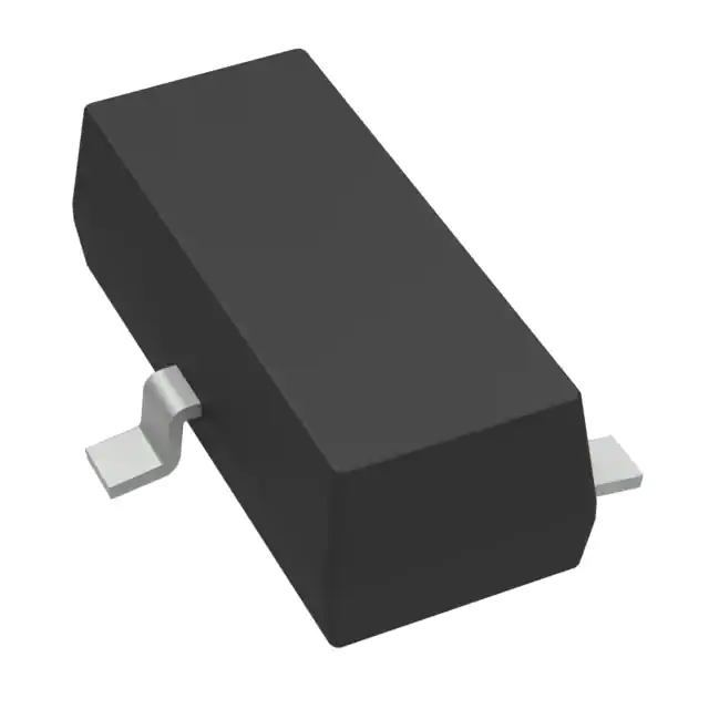
Small Package and Footprint
– Surface Mount 3-Pin SOT-23 (DBZ)
– 2.92 mm × 2.37 mm
– Through-Hole 3-Pin TO-92 (LPG)
– 4.00 mm × 3.15 mm
Protection Features
– Reverse Supply Protection (up to –22 V)
– Supports up to 40-V Load Dump
– Output Short-Circuit Protection
– Output Current Limitation
– OUT Short to Battery Protection
Docking Detection
Door Open and Close Detection
Proximity Sensing
Valve Positioning
Pulse Counting
3 Description
The DRV5023-Q1 device is a chopper-stabilized Hall
Effect Sensor that offers a magnetic sensing solution
with superior sensitivity stability over temperature and
integrated protection features.
When the applied magnetic flux density exceeds the
BOP threshold, the DRV5023-Q1 open-drain output
goes low. The output stays low until the field
decreases to less than BRP, and then the output goes
to high impedance. The output current sink capability
is 30 mA. A wide operating voltage range from 2.7 to
38 V with reverse polarity protection up to –22 V
makes the device suitable for a wide range of
automotive applications.
Internal protection functions are provided for reverse
supply conditions, load dump, and output short circuit
or over current.
Device Information(1)
PART NUMBER
DRV5023-Q1
PACKAGE
BODY SIZE (NOM)
SOT-23 (3)
2.92 mm × 1.30 mm
TO-92 (3)
4.00 mm × 3.15 mm
(1) For all available packages, see the orderable addendum at
the end of the data sheet.
Device Packages
Output State
OUT
Bhys
B (mT)
BRP
BOF
BOP
FA, AJ, and BI Versions
OUT
Bhys
B (mT)
BRP
BOF
BOP
FI Version
1
An IMPORTANT NOTICE at the end of this data sheet addresses availability, warranty, changes, use in safety-critical applications,
intellectual property matters and other important disclaimers. PRODUCTION DATA.
�DRV5023-Q1
SLIS163G – DECEMBER 2014 – REVISED MARCH 2017
www.ti.com
Table of Contents
1
2
3
4
5
6
7
Features ..................................................................
Applications ...........................................................
Description .............................................................
Revision History.....................................................
Pin Configuration and Functions .........................
Specifications.........................................................
1
1
1
2
4
5
6.1
6.2
6.3
6.4
6.5
6.6
6.7
6.8
5
5
5
5
6
6
6
7
Absolute Maximum Ratings ......................................
ESD Ratings..............................................................
Recommended Operating Conditions.......................
Thermal Information ..................................................
Electrical Characteristics...........................................
Switching Characteristics ..........................................
Magnetic Characteristics...........................................
Typical Characteristics ..............................................
Detailed Description .............................................. 9
7.1 Overview ................................................................... 9
7.2 Functional Block Diagram ......................................... 9
7.3 Feature Description................................................. 10
7.4 Device Functional Modes........................................ 15
8
Application and Implementation ........................ 16
8.1 Application Information............................................ 16
8.2 Typical Applications ................................................ 16
9 Power Supply Recommendations...................... 18
10 Layout................................................................... 19
10.1 Layout Guidelines ................................................. 19
10.2 Layout Example .................................................... 19
11 Device and Documentation Support ................. 20
11.1
11.2
11.3
11.4
11.5
11.6
11.7
Device Support......................................................
Documentation Support ........................................
Receiving Notification of Documentation Updates
Community Resources..........................................
Trademarks ...........................................................
Electrostatic Discharge Caution ............................
Glossary ................................................................
20
21
21
21
21
21
21
12 Mechanical, Packaging, and Orderable
Information ........................................................... 21
4 Revision History
NOTE: Page numbers for previous revisions may differ from page numbers in the current version.
Changes from Revision F (September 2016) to Revision G
Page
•
Added the output jitter parameter to the Switching Characteristics table............................................................................... 6
•
Added the Output Jitter Characteristic section ..................................................................................................................... 15
Changes from Revision E (August 2016) to Revision F
•
Page
Made changes to the Power-on time in the Electrical Characteristics table ......................................................................... 6
Changes from Revision D (May 2016) to Revision E
Page
•
Clarified the output description for the FI device version in the Device Output section ...................................................... 10
•
Added the Layout section .................................................................................................................................................... 19
•
Added the Receiving Notification of Documentation Updates section ................................................................................ 21
Changes from Revision C (February 2016) to Revision D
•
Page
Revised preliminary limits for the FA version ......................................................................................................................... 6
Changes from Revision B (December 2015) to Revision C
Page
•
Added the FA and FI device options ..................................................................................................................................... 1
•
Added the typical bandwidth value to the Magnetic Characteristics table ............................................................................ 6
2
Submit Documentation Feedback
Copyright © 2014–2017, Texas Instruments Incorporated
Product Folder Links: DRV5023-Q1
�DRV5023-Q1
www.ti.com
SLIS163G – DECEMBER 2014 – REVISED MARCH 2017
Changes from Revision A (May 2015) to Revision B
Page
•
Corrected body size of SOT-23 package and SIP package name to TO-92 ........................................................................ 1
•
Added BMAX to Absolute Maximum Ratings ........................................................................................................................... 5
•
Removed table notes regarding testing for the operating junction temperature in Absolute Maximum Ratings .................. 5
•
Updated package tape and reel options for M and blank ................................................................................................... 20
•
Added Community Resources ............................................................................................................................................. 21
Changes from Original (December 2014) to Revision A
•
Page
Updated device status to production data ............................................................................................................................. 1
Submit Documentation Feedback
Copyright © 2014–2017, Texas Instruments Incorporated
Product Folder Links: DRV5023-Q1
3
�DRV5023-Q1
SLIS163G – DECEMBER 2014 – REVISED MARCH 2017
www.ti.com
5 Pin Configuration and Functions
For additional configuration information, see Device Markings and Mechanical, Packaging, and Orderable
Information.
DBZ Package
3-Pin SOT-23
Top View
LPG Package
3-Pin TO-92
Top View
OUT
2
3
GND
1
1
2
3
VCC
VCC
OUT
GND
Pin Functions
PIN
NAME
TYPE
DESCRIPTION
DBZ
LPG
GND
3
2
GND
OUT
2
3
Output
Hall sensor open-drain output. The open drain requires a resistor pullup.
VCC
1
1
Power
2.7 to 38 V power supply. Bypass this pin to the GND pin with a 0.01-μF (minimum)
ceramic capacitor rated for VCC.
4
Ground pin
Submit Documentation Feedback
Copyright © 2014–2017, Texas Instruments Incorporated
Product Folder Links: DRV5023-Q1
�DRV5023-Q1
www.ti.com
SLIS163G – DECEMBER 2014 – REVISED MARCH 2017
6 Specifications
6.1 Absolute Maximum Ratings
over operating free-air temperature range (unless otherwise noted) (1)
VCC
Power supply voltage
UNIT
40
V
Unlimited
Output pin voltage
Output pin reverse current during reverse supply condition
Magnetic flux density, BMAX
V/µs
0
2
–0.5
40
V
0
100
mA
Unlimited
Operating junction temperature, TJ
Q, see Figure 26
–40
150
E, see Figure 26
–40
175
–65
150
Storage temperature, Tstg
(2)
MAX
Voltage ramp rate (VCC), VCC < 5 V
Voltage ramp rate (VCC), VCC > 5 V
(1)
MIN
–22 (2)
°C
°C
Stresses beyond those listed under Absolute Maximum Ratings may cause permanent damage to the device. These are stress ratings
only, which do not imply functional operation of the device at these or any other conditions beyond those indicated under Recommended
Operating Conditions. Exposure to absolute-maximum-rated conditions for extended periods may affect device reliability.
Ensured by design. Only tested to –20 V.
6.2 ESD Ratings
VALUE
V(ESD)
(1)
Electrostatic discharge
Human-body model (HBM), per AEC Q100-002 (1)
±2500
Charged-device model (CDM), per AEC Q100-011
±500
UNIT
V
AEC Q100-002 indicates that HBM stressing shall be in accordance with the ANSI/ESDA/JEDEC JS-001 specification.
6.3 Recommended Operating Conditions
over operating free-air temperature range (unless otherwise noted)
MIN MAX
UNIT
VCC
Power supply voltage
2.7
38
VO
Output pin voltage (OUT)
0
38
V
ISINK
Output pin current sink (OUT) (1)
0
30
mA
TA
Operating ambient
temperature
Q, see Figure 26
–40
125
E, see Figure 26
–40
150
(1)
V
°C
Power dissipation and thermal limits must be observed.
6.4 Thermal Information
DRV5023-Q1
THERMAL METRIC (1)
DBZ (SOT-23)
LPG (TO-92)
3 PINS
3 PINS
UNIT
RθJA
Junction-to-ambient thermal resistance
333.2
180
°C/W
RθJC(top)
Junction-to-case (top) thermal resistance
99.9
98.6
°C/W
RθJB
Junction-to-board thermal resistance
66.9
154.9
°C/W
ψJT
Junction-to-top characterization parameter
4.9
40
°C/W
ψJB
Junction-to-board characterization parameter
65.2
154.9
°C/W
(1)
For more information about traditional and new thermal metrics, see the Semiconductor and IC Package Thermal Metrics application
report.
Submit Documentation Feedback
Copyright © 2014–2017, Texas Instruments Incorporated
Product Folder Links: DRV5023-Q1
5
�DRV5023-Q1
SLIS163G – DECEMBER 2014 – REVISED MARCH 2017
www.ti.com
6.5 Electrical Characteristics
over operating free-air temperature range (unless otherwise noted)
PARAMETER
TEST CONDITIONS
MIN
TYP
MAX
UNIT
POWER SUPPLIES (VCC)
VCC
VCC operating voltage
ICC
Operating supply current
ton
Power-on time
2.7
VCC = 2.7 to 38 V, TA = 25°C
38
2.7
VCC = 2.7 to 38 V, TA = TA, MAX (1)
3
3.5
AJ, BI versions
35
50
FA, FI versions
35
70
VCC = 3.3 V, IO = 10 mA, TA = 25°C
22
VCC = 3.3 V, IO = 10 mA, TA = 125°C
36
V
mA
µs
OPEN DRAIN OUTPUT (OUT)
rDS(on)
FET on-resistance
Ilkg(off)
Off-state leakage current
50
Output Hi-Z
Ω
1
µA
45
mA
PROTECTION CIRCUITS
VCCR
Reverse supply voltage
IOCP
Overcurrent protection level
(1)
TA,
MAX
–22
OUT shorted VCC
15
V
30
is 125°C for Q Grade 1 devices and 150°C for E Grade 0 devices (see Figure 26)
6.6 Switching Characteristics
over operating free-air temperature range (unless otherwise noted)
PARAMETER
TEST CONDITIONS
MIN
TYP
MAX
13
25
UNIT
OPEN DRAIN OUTPUT (OUT)
td
Output delay time
B = BRP – 10 mT to BOP + 10 mT in 1 µs
tr
Output rise time (10% to 90%)
R1 = 1 kΩ, CO = 50 pF, VCC = 3.3 V
200
ns
tf
Output fall time (90% to 10%)
R1 = 1 kΩ, CO = 50 pF, VCC = 3.3 V
31
ns
Output jitter
Measured from 20 000 cycles of B increasing
at a rate of 50 mT/ms (see Figure 19)
±8.5
µs
tj
µs
6.7 Magnetic Characteristics
over operating free-air temperature range (unless otherwise noted)
PARAMETER
ƒBW
Bandwidth
TEST CONDITIONS
(2)
MIN
TYP
20
30
MAX
UNIT (1)
kHz
DRV5023FA, DRV5023FI: 3.5 / 2 mT
BOP
Operate point (see Figure 12 and Figure 13)
1.8
3.5
6.8
mT
BRP
Release point (see Figure 12 and Figure 13)
0.5
2
4.2
mT
Bhys
Hysteresis; Bhys= (BOP – BRP)
1.5
mT
BO
Magnetic offset, BO = (BOP + BRP) / 2
2.8
mT
DRV5023AJ: 6.9 / 3.2 mT
BOP
Operate point (see Figure 12 and Figure 13)
3
6.9
12
mT
BRP
Release point (see Figure 12 and Figure 13)
1
3.2
5
mT
Bhys
Hysteresis; Bhys= (BOP – BRP)
BO
Magnetic offset, BO = (BOP + BRP) / 2
3.7
mT
5
mT
DRV5023BI: 14.5 / 6 mT
BOP
Operate point (see Figure 12 and Figure 13)
6
14.5
24
mT
BRP
Release point (see Figure 12 and Figure 13)
3
6
9
mT
Bhys
Hysteresis; Bhys = (BOP – BRP) (3)
BO
Magnetic offset, BO = (BOP + BRP) / 2
(1)
(2)
(3)
6
8.5
mT
10.3
mT
1 mT = 10 Gauss
Bandwidth describes the fastest changing magnetic field that can be detected and translated to the output.
|BOP| is always greater than |BRP|.
Submit Documentation Feedback
Copyright © 2014–2017, Texas Instruments Incorporated
Product Folder Links: DRV5023-Q1
�DRV5023-Q1
www.ti.com
SLIS163G – DECEMBER 2014 – REVISED MARCH 2017
6.8 Typical Characteristics
TA > 125°C data is valid for Grade 0 devices only (E, see Figure 26)
3.5
3.5
TA = 125°C
TA = 150°C
VCC = 3.3 V
VCC = 13.2 V
VCC = 38 V
Supply Current (mA)
Supply Current (mA)
TA ± ƒ&
TA = 25°C
TA = 75°C
3
2.5
2
0
10
20
Supply Voltage (V)
30
3
2.5
2
-50
40
-25
Figure 1. ICC vs VCC
125
150
D010
16
Magnetic Field Operate Point BOP (mT)
Magnetic Field Operate Point BOP (mT)
25
50
75
100
Ambient Temperature (°C)
Figure 2. ICC vs Temperature
16
14
12
DRV5023AJ
DRV5023BI
10
8
6
4
0
10
20
Supply Voltage (V)
30
14
12
DRV5023AJ
DRV5023BI
10
8
6
4
-50
40
-25
0
D001
TA = 25°C
25
50
75
100
Ambient Temperature (°C)
125
150
D002
VCC = 3.3 V
Figure 3. BOP vs VCC
Figure 4. BOP vs Temperature
6.5
7
Magnetic Field Operate Point BRP (mT)
Magnetic Field Release Point BRP (mT)
0
D009
6
5.5
5
4.5
DRV5023BI
DRV5023AJ
4
3.5
3
2.5
2
0
10
20
Supply Voltage (V)
30
TA = 25°C
40
6
5
DRV5023AJ
DRV5023BI
4
3
2
-50
-25
D003
0
25
50
75
100
Ambient Temperature (°C)
125
150
D004
VCC = 3.3 V
Figure 5. BRP vs VCC
Figure 6. BRP vs Temperature
Submit Documentation Feedback
Copyright © 2014–2017, Texas Instruments Incorporated
Product Folder Links: DRV5023-Q1
7
�DRV5023-Q1
SLIS163G – DECEMBER 2014 – REVISED MARCH 2017
www.ti.com
Typical Characteristics (continued)
TA > 125°C data is valid for Grade 0 devices only (E, see Figure 26)
9
10
DRV5023AJ
DRV5023BI
8
8
6
Hysteresis (mT)
Hysteresis (mT)
7
DRV5023AJ
DRV5023BI
5
4
6
4
3
2
0
10
20
Supply Voltage (V)
30
2
-50
40
-25
TA = 25°C
10
10
9
9
8
Offset (mT)
Offset (mT)
11
DRV5023AJ
DRV5023BI
7
8
6
5
5
4
12
16
20
24
28
Supply Voltage (V)
TA = 25°C
32
36
40
4
-50
-25
0
D005
D008
25
50
75
100
Ambient Temperature (°C)
125
150
D006
VCC = 3.3 V
Figure 9. Offset vs VCC
8
150
DRV5023AJ
DRV5023BI
7
6
8
125
Figure 8. Hysteresis vs Temperature
11
4
25
50
75
100
Ambient Temperature (°C)
VCC = 3.3 V
Figure 7. Hysteresis vs VCC
0
0
D007
Figure 10. Offset vs Temperature
Submit Documentation Feedback
Copyright © 2014–2017, Texas Instruments Incorporated
Product Folder Links: DRV5023-Q1
�DRV5023-Q1
www.ti.com
SLIS163G – DECEMBER 2014 – REVISED MARCH 2017
7 Detailed Description
7.1 Overview
The DRV5023-Q1 device is a chopper-stabilized Hall sensor with a digital output for magnetic sensing
applications. The DRV5023-Q1 device can be powered with a supply voltage between 2.7 and 38 V, and will
survive –22 V reverse-battery conditions. The DRV5023-Q1 device does not operate when –22 to 2.4 V is
applied to the VCC pin (with respect to GND pin). In addition, the device can withstand supply voltages up to 40 V
for transient durations.
The field polarity is defined as follows: a south pole near the marked side of the package is a positive magnetic
field. A north pole near the marked side of the package is a negative magnetic field. The output state is
dependent on the magnetic field perpendicular to the package.
For the FA, AJ, and BI device versions, a strong south pole near the marked side of the package causes the
output to pull low, and the absence of a field makes the output high-impedance. The FI version has an inverted
output response, where a strong south pole causes the output to be high-impedance, and the absence of a field
makes the output pull low. Hysteresis is included in between the operate point and the release point to prevent
toggling near the magnetic threshold.
An external pullup resistor is required on the OUT pin. The OUT pin can be pulled up to VCC, or to a different
voltage supply. This allows for easier interfacing with controller circuits.
7.2 Functional Block Diagram
2.7 V to 38 V
C1
VCC
Regulated Supply
Bias
R1
Temperature
Compensation
OUT
C2
OCP
Offset Cancel
Hall Element
(Optional)
+
Gate
Drive
±
Reference
GND
Submit Documentation Feedback
Copyright © 2014–2017, Texas Instruments Incorporated
Product Folder Links: DRV5023-Q1
9
�DRV5023-Q1
SLIS163G – DECEMBER 2014 – REVISED MARCH 2017
www.ti.com
7.3 Feature Description
7.3.1 Field Direction Definition
A positive magnetic field is defined as a south pole near the marked side of the package as shown in Figure 11.
SOT-23 (DBZ)
TO-92 (LPG)
B > 0 mT
B < 0 mT
B > 0 mT
B < 0 mT
N
S
N
S
S
N
S
N
1
2
3
1
2
3
(Bottom view)
N = North pole, S = South pole
Figure 11. Field Direction Definition
7.3.2 Device Output
If the device is powered on with a magnetic field strength between BRP and BOP, then the device output is
indeterminate and can either be Hi-Z or Low. For the FA, AJ, and BI device versions, if the field strength is
greater than BOP, then the output is pulled low; if the field strength is less than BRP, then the output is released.
For the FI device version, if the field strength is greater than BOP, then the output is Hi-Z; if the field strength is
less than BRP, then the output is pulled Low.
OUT
Bhys
B (mT)
BRP
BOF
BOP
Figure 12. Output State of FA, AJ, BI Versions
OUT
Bhys
B (mT)
BRP
BOF
BOP
Figure 13. Output State of FI Version
10
Submit Documentation Feedback
Copyright © 2014–2017, Texas Instruments Incorporated
Product Folder Links: DRV5023-Q1
�DRV5023-Q1
www.ti.com
SLIS163G – DECEMBER 2014 – REVISED MARCH 2017
Feature Description (continued)
7.3.3 Power-On Time
After applying VCC to the DRV5023-Q1 device, ton must elapse before the OUT pin is valid. During the power-up
sequence, the output is Hi-Z. A pulse as shown in Figure 14 and Figure 15 occurs at the end of ton. This pulse
can allow the host processor to determine when the DRV5023-Q1 output is valid after startup. In Case 1
(Figure 14) and Case 2 (Figure 15), the output is defined assuming a constant magnetic field B > BOP and B <
BRP.
VCC
t (s)
B (mT)
BOP
BRP
t (s)
OUT
Valid Output
t (s)
ton
Figure 14. Case 1: Power On When B > BOP
VCC
t (s)
B (mT)
BOP
BRP
t (s)
OUT
Valid Output
t (s)
ton
Figure 15. Case 2: Power On When B < BRP
Submit Documentation Feedback
Copyright © 2014–2017, Texas Instruments Incorporated
Product Folder Links: DRV5023-Q1
11
�DRV5023-Q1
SLIS163G – DECEMBER 2014 – REVISED MARCH 2017
www.ti.com
Feature Description (continued)
If the device is powered on with the magnetic field strength BRP < B < BOP, then the device output is
indeterminate and can either be Hi-Z or pulled low. During the power-up sequence, the output is held Hi-Z until
ton has elapsed. At the end of ton, a pulse is given on the OUT pin to indicate that ton has elapsed. After ton, if the
magnetic field changes such that BOP < B, the output is released. Case 3 (Figure 16) and Case 4 (Figure 17)
show examples of this behavior.
VCC
t (s)
B (mT)
BOP
BRP
t (s)
OUT
Valid Output
t (s)
ton
td
Figure 16. Case 3: Power On When BRP < B < BOP, Followed by B > BOP
12
Submit Documentation Feedback
Copyright © 2014–2017, Texas Instruments Incorporated
Product Folder Links: DRV5023-Q1
�DRV5023-Q1
www.ti.com
SLIS163G – DECEMBER 2014 – REVISED MARCH 2017
Feature Description (continued)
VCC
t (s)
B (mT)
BOP
BRP
t (s)
OUT
Valid Output
t (s)
ton
td
Figure 17. Case 4: Power On When BRP < B < BOP, Followed by B < BRP
Submit Documentation Feedback
Copyright © 2014–2017, Texas Instruments Incorporated
Product Folder Links: DRV5023-Q1
13
�DRV5023-Q1
SLIS163G – DECEMBER 2014 – REVISED MARCH 2017
www.ti.com
Feature Description (continued)
7.3.4 Output Stage
The DRV5023-Q1 output stage uses an open-drain NMOS, and it is rated to sink up to 30 mA of current. For
proper operation, calculate the value of the pullup resistor R1 using Equation 1.
Vref max
V min
d R1 d ref
30 mA
100 µA
(1)
The size of R1 is a tradeoff between the OUT rise time and the current when OUT is pulled low. A lower current
is generally better, however faster transitions and bandwidth require a smaller resistor for faster switching.
In addition, ensure that the value of R1 > 500 Ω to ensure the output driver can pull the OUT pin close to GND.
NOTE
Vref is not restricted to VCC. The allowable voltage range of this pin is specified in the
Absolute Maximum Ratings.
Vref
R1
OUT
ISINK
OCP
C2
Gate
Drive
GND
Figure 18.
Select a value for C2 based on the system bandwidth specifications as shown in Equation 2.
1
u ¦BW +]
2S u R1 u C2
(2)
Most applications do not require this C2 filtering capacitor.
14
Submit Documentation Feedback
Copyright © 2014–2017, Texas Instruments Incorporated
Product Folder Links: DRV5023-Q1
�DRV5023-Q1
www.ti.com
SLIS163G – DECEMBER 2014 – REVISED MARCH 2017
Feature Description (continued)
7.3.5 Protection Circuits
The DRV5023-Q1 device is fully protected against overcurrent and reverse-supply conditions.
7.3.5.1 Overcurrent Protection (OCP)
An analog current-limit circuit limits the current through the FET. The driver current is clamped to IOCP. During
this clamping, the rDS(on) of the output FET is increased from the nominal value.
7.3.5.2 Load Dump Protection
The DRV5023-Q1 device operates at DC VCC conditions up to 38 V nominally, and can additionally withstand
VCC = 40 V. No current-limiting series resistor is required for this protection.
7.3.5.3 Reverse Supply Protection
The DRV5023-Q1 device is protected in the event that the VCC pin and the GND pin are reversed (up to –22 V).
NOTE
In a reverse supply condition, the OUT pin reverse-current must not exceed the ratings
specified in the Absolute Maximum Ratings.
Table 1.
FAULT
CONDITION
DEVICE
DESCRIPTION
RECOVERY
FET overload (OCP)
ISINK ≥ IOCP
Operating
Output current is clamped to IOCP
IO < IOCP
Load dump
38 V < VCC < 40 V
Operating
Device will operate for a transient duration
VCC ≤ 38 V
Reverse supply
–22 V < VCC < 0 V
Disabled
Device will survive this condition
VCC ≥ 2.7 V
7.3.5.4 Output Jitter Characteristic
The DRV5023-Q1 propagation delay is not fully consistent. If a periodic magnetic field is applied, the device
introduces a small amount of jitter on the output. The tj parameter describes this characteristic and Figure 19
shows the test waveform.
B
Cycle 1
Cycle 2
Cycle 3
BOP
time
Figure 19. Test Waveform for tj
7.4 Device Functional Modes
The DRV5023-Q1 device is active only when VCC is between 2.7 and 38 V.
When a reverse supply condition exists, the device is inactive.
Submit Documentation Feedback
Copyright © 2014–2017, Texas Instruments Incorporated
Product Folder Links: DRV5023-Q1
15
�DRV5023-Q1
SLIS163G – DECEMBER 2014 – REVISED MARCH 2017
www.ti.com
8 Application and Implementation
NOTE
Information in the following applications sections is not part of the TI component
specification, and TI does not warrant its accuracy or completeness. TI’s customers are
responsible for determining suitability of components for their purposes. Customers should
validate and test their design implementation to confirm system functionality.
8.1 Application Information
The DRV5023-Q1 device is used in magnetic-field sensing applications.
8.2 Typical Applications
8.2.1 Standard Circuit
C2
680 pF
(Optional)
2
OUT
R1
10 kŸ
3
1
VCC
VCC
C1
0.01 µF
(minimum)
Figure 20. Typical Application Circuit
8.2.1.1 Design Requirements
For this design example, use the parameters listed in Table 2 as the input parameters.
Table 2. Design Parameters
DESIGN PARAMETER
REFERENCE
EXAMPLE VALUE
Supply voltage
VCC
3.2 to 3.4 V
System bandwidth
ƒBW
10 kHz
8.2.1.2 Detailed Design Procedure
Table 3. External Components
COMPONENT
(1)
16
PIN 1
PIN 2
RECOMMENDED
C1
VCC
GND
A 0.01-µF (minimum) ceramic capacitor rated for VCC
C2
OUT
GND
Optional: Place a ceramic capacitor to GND
R1
OUT
REF (1)
Requires a resistor pullup
REF is not a pin on the DRV5023-Q1 device, but a REF supply-voltage pullup is required for the OUT pin; the OUT pin may be pulled
up to VCC.
Submit Documentation Feedback
Copyright © 2014–2017, Texas Instruments Incorporated
Product Folder Links: DRV5023-Q1
�DRV5023-Q1
www.ti.com
SLIS163G – DECEMBER 2014 – REVISED MARCH 2017
8.2.1.2.1 Configuration Example
In a 3.3-V system, 3.2 V ≤ Vref ≤ 3.4 V. Use Equation 3 to calculate the allowable range for R1.
Vref max
V min
d R1 d ref
30 mA
100 µA
(3)
For this design example, use Equation 4 to calculate the allowable range of R1.
3.4 V
3.2 V
d R1 d
30 mA
100 µA
(4)
Therefore:
113 Ω ≤ R1 ≤ 32 kΩ
(5)
After finding the allowable range of R1 (Equation 5), select a value between 500 Ω and 32 kΩ for R1.
Assuming a system bandwidth of 10 kHz, use Equation 6 to calculate the value of C2.
1
u ¦BW +]
2S u R1 u C2
(6)
For this design example, use Equation 7 to calculate the value of C2.
1
2 u 10 kHz
2S u R1 u C2
(7)
An R1 value of 10 kΩ and a C2 value less than 820 pF satisfy the requirement for a 10-kHz system bandwidth.
A selection of R1 = 10 kΩ and C2 = 680 pF would cause a low-pass filter with a corner frequency of 23.4 kHz.
8.2.1.3 Application Curves
OUT
OUT
R1 = 10-kΩ pullup
R1 = 10-kΩ pullup
No C2
C2 = 680 pF
Figure 22. 10-kHz Switching Magnetic Field
Figure 21. 10-kHz Switching Magnetic Field
0
-2
Magnitude (dB)
-4
-6
-8
-10
-12
-14
100
1000
10000
Frequency (Hz)
R1 = 10-kΩ pullup
100000
D011
C2 = 680 pF
Figure 23. Low-Pass Filtering
Submit Documentation Feedback
Copyright © 2014–2017, Texas Instruments Incorporated
Product Folder Links: DRV5023-Q1
17
�DRV5023-Q1
SLIS163G – DECEMBER 2014 – REVISED MARCH 2017
www.ti.com
8.2.2 Alternative Two-Wire Application
For systems that require minimal wire count, the device output can be connected to VCC through a resistor, and
the total supplied current can be sensed near the controller.
R1
+
OUT 2
±
VCC 1
C1
GND
3
Current
sense
Controller
Figure 24. 2-Wire Application
Current can be sensed using a shunt resistor or other circuitry.
8.2.2.1 Design Requirements
Table 4 lists the related design parameters.
Table 4. Design Parameters
REFERENCE
EXAMPLE VALUE
Supply voltage
DESIGN PARAMETER
VCC
12 V
OUT resistor
R1
1 kΩ
Bypass capacitor
C1
0.1 µF
Current when B < BRP
IRELEASE
About 3 mA
Current when B > BOP
IOPERATE
About 15 mA
8.2.2.2 Detailed Design Procedure
When the open-drain output of the device is high-impedance, current through the path equals the ICC of the
device (approximately 3 mA).
When the output pulls low, a parallel current path is added, equal to VCC / (R1 + rDS(on)). Using 12 V and 1 kΩ,
the parallel current is approximately 12 mA, making the total current approximately 15 mA.
The local bypass capacitor C1 should be at least 0.1 µF, and a larger value if there is high inductance in the
power line interconnect.
9 Power Supply Recommendations
The DRV5023-Q1 device is designed to operate from an input voltage supply (VM) range between 2.7 and 38 V.
A 0.01-µF (minimum) ceramic capacitor rated for VCC must be placed as close to the DRV5023-Q1 device as
possible.
18
Submit Documentation Feedback
Copyright © 2014–2017, Texas Instruments Incorporated
Product Folder Links: DRV5023-Q1
�DRV5023-Q1
www.ti.com
SLIS163G – DECEMBER 2014 – REVISED MARCH 2017
10 Layout
10.1 Layout Guidelines
The bypass capacitor should be placed near the DRV5023-Q1 device for efficient power delivery with minimal
inductance. The external pullup resistor should be placed near the microcontroller input to provide the most
stable voltage at the input; alternatively, an integrated pullup resistor within the GPIO of the microcontroller can
be used.
Generally, using PCB copper planes underneath the DRV5023-Q1 device has no effect on magnetic flux, and
does not interfere with device performance. This is because copper is not a ferromagnetic material. However, If
nearby system components contain iron or nickel, they may redirect magnetic flux in unpredictable ways.
10.2 Layout Example
VCC
OUT
GND
Figure 25. DRV5023-Q1 Layout Example
Submit Documentation Feedback
Copyright © 2014–2017, Texas Instruments Incorporated
Product Folder Links: DRV5023-Q1
19
�DRV5023-Q1
SLIS163G – DECEMBER 2014 – REVISED MARCH 2017
www.ti.com
11 Device and Documentation Support
11.1 Device Support
11.1.1 Device Nomenclature
Figure 26 shows a legend for reading the complete device name for and DRV5023-Q1 device.
DRV5023
(AJ)
(Q)
(DBZ)
(R)
(Q1)
Prefix
DRV5023: Digital switch Hall sensor
AEC-Q100
Q1: Automotive qualification
Blank: Non-auto
BOP/BRP
FA: 3.5/2 mT
FI: 3.5/2 mT, inverter
AJ: 6.9/3.2 mT
BI: 14.5/6 mT
Tape and Reel
R: 3000 pcs/reel
T: 250 pcs/reel
M: 3000 pcs/box (ammo)
Blank: 1000 pcs/bag (bulk
Package
DBZ: 3-pin SOT-23
LPG: 3-pin TO-92
Temperature Range
Q: ±40 to 125°C
E: ±40 to 150°C
Figure 26. Device Nomenclature
11.1.2 Device Markings
Marked Side
3
Marked Side Front
1
1
2
3
2
Marked Side
1
2
3
(Bottom view)
Figure 27. SOT-23 (DBZ) Package
Figure 28. TO-92 (LPG) Package
indicates the Hall effect sensor (not to scale). The Hall element is located in the center of the package with a
tolerance of ±100 µm. The height of the Hall element from the bottom of the package is 0.7 mm ±50 µm in the DBZ
package and 0.987 mm ±50 µm in the LPG package.
20
Submit Documentation Feedback
Copyright © 2014–2017, Texas Instruments Incorporated
Product Folder Links: DRV5023-Q1
�DRV5023-Q1
www.ti.com
SLIS163G – DECEMBER 2014 – REVISED MARCH 2017
11.2 Documentation Support
11.2.1 Related Documentation
For related documentation see the following:
Understanding & Applying Hall Effect Sensor Datasheets
11.3 Receiving Notification of Documentation Updates
To receive notification of documentation updates, navigate to the device product folder on ti.com. In the upper
right corner, click on Alert me to register and receive a weekly digest of any product information that has
changed. For change details, review the revision history included in any revised document.
11.4 Community Resources
The following links connect to TI community resources. Linked contents are provided "AS IS" by the respective
contributors. They do not constitute TI specifications and do not necessarily reflect TI's views; see TI's Terms of
Use.
TI E2E™ Online Community TI's Engineer-to-Engineer (E2E) Community. Created to foster collaboration
among engineers. At e2e.ti.com, you can ask questions, share knowledge, explore ideas and help
solve problems with fellow engineers.
Design Support TI's Design Support Quickly find helpful E2E forums along with design support tools and
contact information for technical support.
11.5 Trademarks
E2E is a trademark of Texas Instruments.
All other trademarks are the property of their respective owners.
11.6 Electrostatic Discharge Caution
These devices have limited built-in ESD protection. The leads should be shorted together or the device placed in conductive foam
during storage or handling to prevent electrostatic damage to the MOS gates.
11.7 Glossary
SLYZ022 — TI Glossary.
This glossary lists and explains terms, acronyms, and definitions.
12 Mechanical, Packaging, and Orderable Information
The following pages include mechanical, packaging, and orderable information. This information is the most
current data available for the designated devices. This data is subject to change without notice and revision of
this document. For browser-based versions of this data sheet, refer to the left-hand navigation.
Submit Documentation Feedback
Copyright © 2014–2017, Texas Instruments Incorporated
Product Folder Links: DRV5023-Q1
21
�PACKAGE OPTION ADDENDUM
www.ti.com
10-Dec-2020
PACKAGING INFORMATION
Orderable Device
Status
(1)
Package Type Package Pins Package
Drawing
Qty
Eco Plan
(2)
Lead finish/
Ball material
MSL Peak Temp
Op Temp (°C)
Device Marking
(3)
(4/5)
(6)
DRV5023AJEDBZRQ1
ACTIVE
SOT-23
DBZ
3
3000
RoHS & Green
NIPDAUAG
Level-1-260C-UNLIM
-40 to 150
+PJAJ
DRV5023AJEDBZTQ1
ACTIVE
SOT-23
DBZ
3
250
RoHS & Green
NIPDAUAG
Level-1-260C-UNLIM
-40 to 150
+PJAJ
DRV5023AJELPGMQ1
ACTIVE
TO-92
LPG
3
3000
RoHS & Green
SN
N / A for Pkg Type
-40 to 150
+PJAJ
DRV5023AJELPGQ1
ACTIVE
TO-92
LPG
3
1000
RoHS & Green
SN
N / A for Pkg Type
-40 to 150
+PJAJ
DRV5023AJQDBZRQ1
ACTIVE
SOT-23
DBZ
3
3000
RoHS & Green
NIPDAUAG
Level-1-260C-UNLIM
-40 to 125
+PKAJ
DRV5023AJQDBZTQ1
ACTIVE
SOT-23
DBZ
3
250
RoHS & Green
NIPDAUAG
Level-1-260C-UNLIM
-40 to 125
+PKAJ
DRV5023AJQLPGMQ1
ACTIVE
TO-92
LPG
3
3000
RoHS & Green
SN
N / A for Pkg Type
-40 to 125
+PKAJ
DRV5023AJQLPGQ1
ACTIVE
TO-92
LPG
3
1000
RoHS & Green
SN
N / A for Pkg Type
-40 to 125
+PKAJ
DRV5023BIEDBZRQ1
ACTIVE
SOT-23
DBZ
3
3000
RoHS & Green
NIPDAUAG
Level-1-260C-UNLIM
-40 to 150
+PJBI
DRV5023BIEDBZTQ1
ACTIVE
SOT-23
DBZ
3
250
RoHS & Green
NIPDAUAG
Level-1-260C-UNLIM
-40 to 150
+PJBI
DRV5023BIELPGMQ1
ACTIVE
TO-92
LPG
3
3000
RoHS & Green
SN
N / A for Pkg Type
-40 to 150
+PJBI
DRV5023BIELPGQ1
ACTIVE
TO-92
LPG
3
1000
RoHS & Green
SN
N / A for Pkg Type
-40 to 150
+PJBI
DRV5023BIQDBZRQ1
ACTIVE
SOT-23
DBZ
3
3000
RoHS & Green
NIPDAUAG
Level-1-260C-UNLIM
-40 to 125
+PKBI
DRV5023BIQDBZTQ1
ACTIVE
SOT-23
DBZ
3
250
RoHS & Green
NIPDAUAG
Level-1-260C-UNLIM
-40 to 125
+PKBI
DRV5023BIQLPGMQ1
ACTIVE
TO-92
LPG
3
3000
RoHS & Green
SN
N / A for Pkg Type
-40 to 125
+PKBI
DRV5023BIQLPGQ1
ACTIVE
TO-92
LPG
3
1000
RoHS & Green
SN
N / A for Pkg Type
-40 to 125
+PKBI
DRV5023FAEDBZRQ1
ACTIVE
SOT-23
DBZ
3
3000
RoHS & Green
SN
Level-1-260C-UNLIM
-40 to 150
+PJFA
DRV5023FIEDBZRQ1
ACTIVE
SOT-23
DBZ
3
3000
RoHS & Green
SN
Level-1-260C-UNLIM
-40 to 150
+PJFI
(1)
The marketing status values are defined as follows:
ACTIVE: Product device recommended for new designs.
LIFEBUY: TI has announced that the device will be discontinued, and a lifetime-buy period is in effect.
Addendum-Page 1
Samples
�PACKAGE OPTION ADDENDUM
www.ti.com
10-Dec-2020
NRND: Not recommended for new designs. Device is in production to support existing customers, but TI does not recommend using this part in a new design.
PREVIEW: Device has been announced but is not in production. Samples may or may not be available.
OBSOLETE: TI has discontinued the production of the device.
(2)
RoHS: TI defines "RoHS" to mean semiconductor products that are compliant with the current EU RoHS requirements for all 10 RoHS substances, including the requirement that RoHS substance
do not exceed 0.1% by weight in homogeneous materials. Where designed to be soldered at high temperatures, "RoHS" products are suitable for use in specified lead-free processes. TI may
reference these types of products as "Pb-Free".
RoHS Exempt: TI defines "RoHS Exempt" to mean products that contain lead but are compliant with EU RoHS pursuant to a specific EU RoHS exemption.
Green: TI defines "Green" to mean the content of Chlorine (Cl) and Bromine (Br) based flame retardants meet JS709B low halogen requirements of


 工商网监
湘ICP备2023018690号
工商网监
湘ICP备2023018690号
